Development of ninp largearea silicon microstrip sensors for

- Slides: 23

Development of n-in-p large-area silicon microstrip sensors for very high radiation environments Y. Unno for the ATLAS 12 sensor community and Hamamatsu Photonics K. K. 2013/9/3, HSTD 9, Y. Unno 1

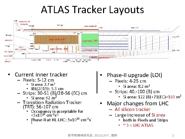
ATLAS Tracker Layouts • Current inner tracker • Phase-II upgrade (LOI) – Pixels: 5 -12 cm – Pixels: 4 -25 cm • Si area: 2. 7 m 2 • Si area: 8. 2 m 2 • IBL(2015): 3. 3 cm – Strips: 30 -51 (B)/28 -56 (EC) cm • Si area: 62 m 2 – Transition Radiation Tracker (TRT): 56 -107 cm • Occupancy is acceptable for <3 x 1034 cm-2 s-1 • Phase-II at HL-LHC: 5 x 1034 cm-2 s- – Strips: 40. -100 (B) cm • Si area: 122 (B)+71(EC)=193 m 2 • Major changes from LHC – All silicon tracker – Large increase of Si area 1 新学術領域研究会、2012/1/6 -7、海野 • both in Pixels and Strips • ~ 3 × LHC ATLAS 2

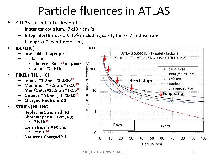
Particle fluences in ATLAS • ATLAS detector to design for • – Instantaneous lum. : 7 x 1034 cm-2 s-1 – Integrated lum. : 6000 fb-1 (including safety factor 2 in dose rate) – Pileup: 200 events/crossing IBL (LHC) • PIXELs (HL-LHC) • – Insertable B-layer pixel – r = 3. 3 cm • Flunece ~3 x 10¹⁵ neq/cm 2 • at Int. L~300 fb-1 – – – Short strips Inner: r=3. 7 cm ~2. 2 x 10¹⁶ Medium: r = 7. 5 cm, ~6 x 10¹⁵ Med/Out: r=15. 5 cm ~2 x 10¹⁵ Outer: r = 31 cm (? ) ~1 x 10¹⁵ Charged: Neutrons ≥ 1 Long strips STRIPs (HL-LHC) – Replacing Strip and TRT – Short strip: r = 30 cm, e. g. • ~1 x 10¹⁵ – Long strips: r = 60 cm, • ~5× 10¹⁴ – Neutrons: Charged ≥ 1 2012/11/18 Y. Unno, M. Mikuz 3

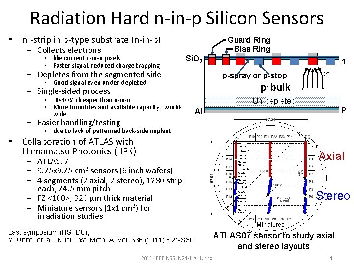
Radiation Hard n-in-p Silicon Sensors • n+-strip in p-type substrate (n-in-p) – Collects electrons • like current n-in-n pixels • Faster signal, reduced charge trapping Guard Ring Bias Ring Si. O 2 – Depletes from the segmented side p-spray or p-stop • Good signal even under-depleted e- p- bulk – Single-sided process • 30 -40% cheaper than n-in-n • More foundries and available capacity worldwide n+ Un-depleted p+ Al – Easier handling/testing • due to lack of patterned back-side implant • Collaboration of ATLAS with Hamamatsu Photonics (HPK) Axial – ATLAS 07 – 9. 75 x 9. 75 cm 2 sensors (6 inch wafers) – 4 segments (2 axial, 2 stereo), 1280 strip each, 74. 5 mm pitch – FZ <100>, 320 µm thick material – Miniature sensors (1 x 1 cm 2) for irradiation studies Last symposium (HSTD 8), Y. Unno, et. al. , Nucl. Inst. Meth. A, Vol. 636 (2011) S 24 -S 30 2011 IEEE NSS, N 24 -1 Y. Unno Stereo Miniatures ATLAS 07 sensor to study axial and stereo layouts 4

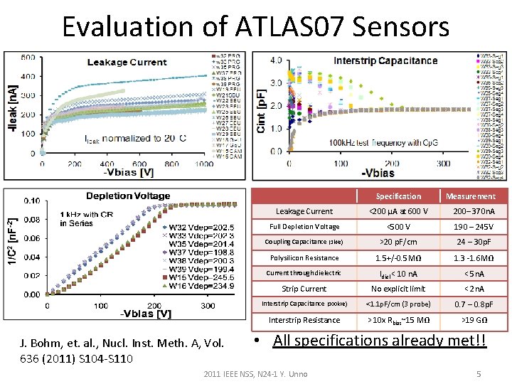
Evaluation of ATLAS 07 Sensors Specification J. Bohm, et. al. , Nucl. Inst. Meth. A, Vol. 636 (2011) S 104 -S 110 Measurement Leakage Current <200 µA at 600 V 200– 370 n. A Full Depletion Voltage <500 V 190 – 245 V Coupling Capacitance (1 k. Hz) >20 p. F/cm 24 – 30 p. F Polysilicon Resistance 1. 5+/-0. 5 MΩ 1. 3 -1. 6 MΩ Current through dielectric Idiel < 10 n. A < 5 n. A Strip Current No explicit limit < 2 n. A Interstrip Capacitance (100 k. Hz) <1. 1 p. F/cm (3 probe) 0. 7 – 0. 8 p. F Interstrip Resistance > 10 x Rbias~15 MΩ >19 GΩ • All specifications already met!! 2011 IEEE NSS, N 24 -1 Y. Unno 5

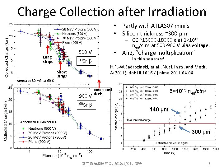
Charge Collection after Irradiation • Partly with ATLAS 07 mini’s • Silicon thickness ~300 µm 500 V Long strips Annealed 80 min at 60 C – CC ~13000 -18000 e at 1× 10¹⁵ neq/cm 2 at 500 -900 V bias voltage. 90 Sr b Short strips 900 V 90 Sr • And, “Charge multiplication” – in thin sensors? H. F. -W. Sadrozinski, et al. , Nucl. Instr. and Meth. A(2011), doi: 10. 1016 / j. nima. 2011. 04. 06 Inner-most pixels b 5× 10¹⁵ neq/cm 2 140 µm Annealed 80 min at 60 C 300 µm 新学術領域研究会、2012/1/6 -7、海野 6

R&D’s in Other Wafers • In the meantime, other R&D’s were: (1) Punchthrough protection (PTP) structures (2) Least-wide edge region (“slim edge”) - HSTD 8, PIXEL 2012 S. Mitsui et al. , Nucl. Instr. Meth. A 699 (2013) 36 -40 Y. Unno et al. , Nucl. Instr. Meth. A 699 (2013) 72 -77 Y. Unno et al. , Nucl. Instr. Meth. (2013) http: //dx. doi. org/10. 1016/j. nima. 2013. 04. 075 i (1) Mitigation of “Stereo” dead area - This ATLAS 12 sensors 2013/9/3, HSTD 9, Y. Unno 7

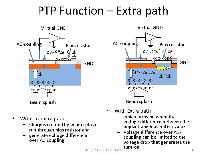
PTP Function – Extra path Virtual GND AC-coupling Bias resistor ∆V=R*∆I ← ∆I → xxxxx GND Virtual GND AC-coupling Bias resistor ∆v=R*∆i ← ∆i → xxxxx GND e- e- ee- e- e- ∆I (=∆I’+∆i) ∆I’>∆i e- e- ee- e- e- Beam splash ∆I • With Extra path – which turns on when the voltage difference between the – Charges created by beam splash implant and bias rail is > onset. – run through bias resistor and – Voltage difference over AC– generate voltage difference coupling can be limited to the over AC coupling voltage drop that generates the turn-on. 2013/9/3, HSTD 9, Y. Unno • Without extra path 8

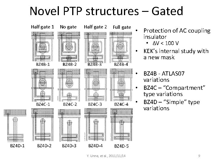
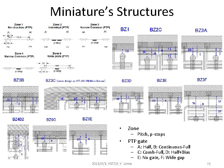
Novel PTP structures – Gated Half gate 1 No gate Half gate 2 Full gate • Protection of AC coupling insulator • ∆V < 100 V • KEK’s internal study with a new mask • BZ 4 B - ATLAS 07 variations • BZ 4 C – “Compartment” type variations • BZ 4 D – “Simple” type variations Y. Unno, et al. , 2011/11/14 9

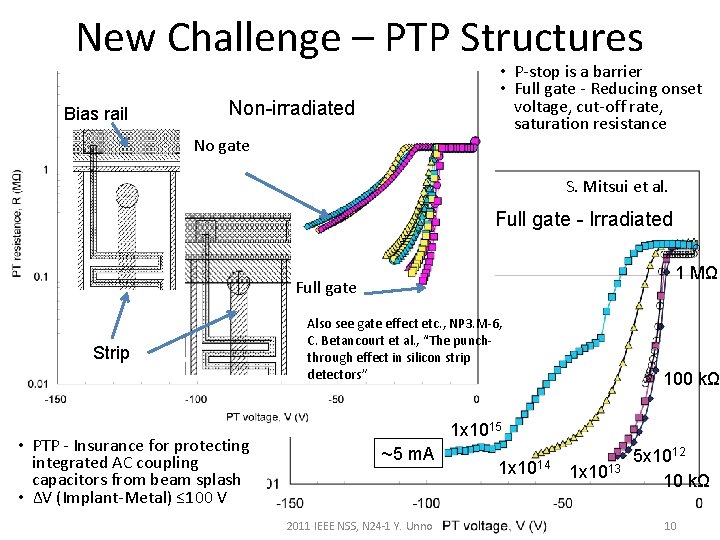
New Challenge – PTP Structures Bias rail • P-stop is a barrier • Full gate - Reducing onset voltage, cut-off rate, saturation resistance Non-irradiated No gate S. Mitsui et al. Full gate - Irradiated 1 MΩ Full gate Strip • PTP - Insurance for protecting integrated AC coupling capacitors from beam splash • ∆V (Implant-Metal) ≤ 100 V Also see gate effect etc. , NP 3. M-6, C. Betancourt et al. , “The punchthrough effect in silicon strip detectors” 100 kΩ 1 x 10¹⁵ ~5 m. A 2011 IEEE NSS, N 24 -1 Y. Unno 1 x 10¹⁴ 1 x 10¹³ 5 x 10¹² 10 kΩ 10

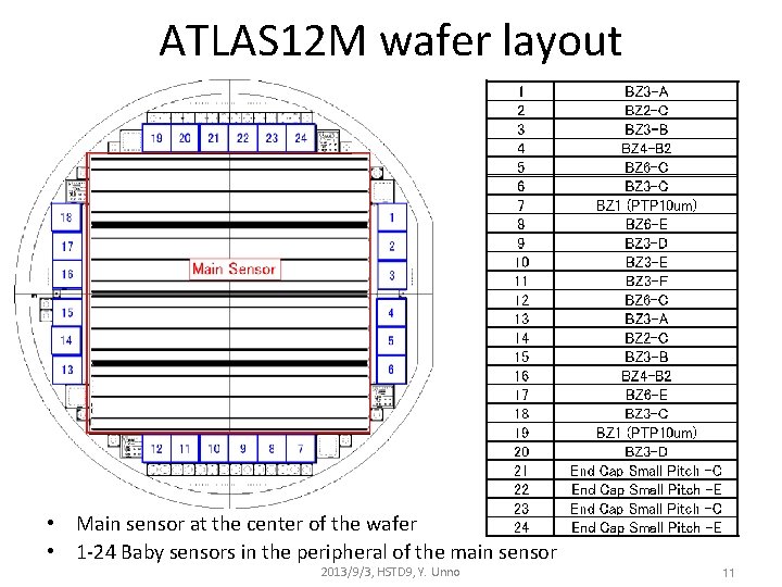
ATLAS 12 M wafer layout • Main sensor at the center of the wafer • 1 -24 Baby sensors in the peripheral of the main sensor 2013/9/3, HSTD 9, Y. Unno 11

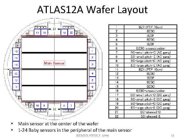
ATLAS 12 A Wafer Layout • Main sensor at the center of the wafer • 1 -24 Baby sensors in the peripheral of the main sensor 2013/9/3, HSTD 9, Y. Unno 12

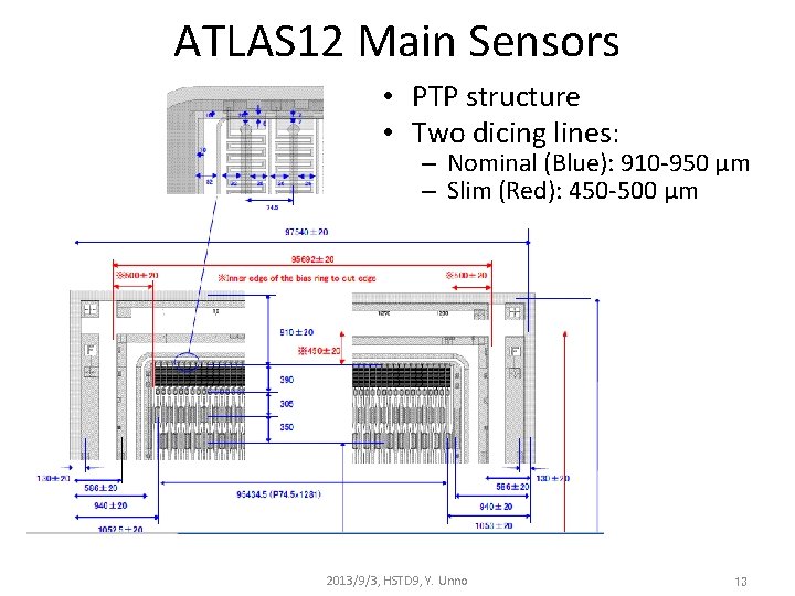
ATLAS 12 Main Sensors • PTP structure • Two dicing lines: – Nominal (Blue): 910 -950 µm – Slim (Red): 450 -500 µm 2013/9/3, HSTD 9, Y. Unno 13

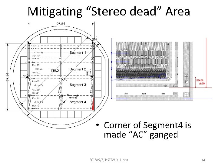
Mitigating “Stereo dead” Area • Corner of Segment 4 is made “AC” ganged 2013/9/3, HSTD 9, Y. Unno 14

Miniature’s Structures • Zone • PTP gate – Pitch, p-stops – A: Half, B: Continuous-Full – C: Comb-Full, D: Half+Bias – E: No gate, F: Wide gap 2013/9/3, HSTD 9, Y. Unno 15

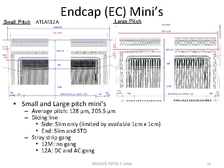
ATLAS 12 A Endcap (EC) Mini’s • Small and Large pitch mini’s – Average pitch: 128 µm, 205. 5 µm – Dicing line • Side: Slim only (limited by available 1 cm x 1 cm) • End: Slim and STD – Stray strip gang • 12 M: no gang • 12 A: DC and AC gang 2013/9/3, HSTD 9, Y. Unno 16

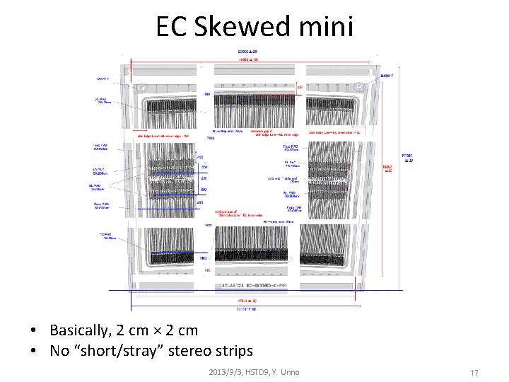
EC Skewed mini • Basically, 2 cm × 2 cm • No “short/stray” stereo strips 2013/9/3, HSTD 9, Y. Unno 17

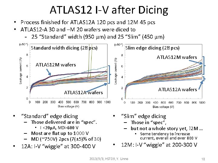
ATLAS 12 I-V after Dicing • Process finished for ATLAS 12 A 120 pcs and 12 M 45 pcs • ATLAS 12 -A 30 and –M 20 wafers were diced to - 25 “Standard” width (950 µm) and 25 “Slim” (450 µm) Standard width dicing (28 pcs) Slim edge dicing (28 pcs) ATLAS 12 M wafers ATLAS 12 A wafers • “Standard” edge dicing – Those delivered are in “spec”. • I <20µA, MD>600 V – Most are flat up to 1000 V – MD (~750 V) 2 pcs (7(± 5)% of 30) • 12 A: I-V “wiggle” at 300 -400 V • “Slim” edge dicing – Those in “spec”, – but not a whole story yet, !2 M … • Some tendency to increase current, overall and over 800 V • 12 M: I-V “wiggle” at 200 -300 V 2013/9/3, HSTD 9, Y. Unno 18

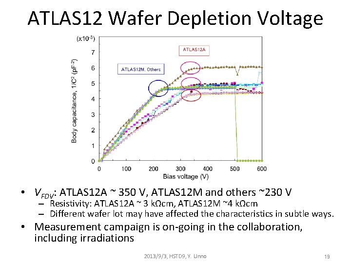
ATLAS 12 Wafer Depletion Voltage • VFDV: ATLAS 12 A ~ 350 V, ATLAS 12 M and others ~230 V – Resistivity: ATLAS 12 A ~ 3 kΩcm, ATLAS 12 M ~4 kΩcm – Different wafer lot may have affected the characteristics in subtle ways. • Measurement campaign is on-going in the collaboration, including irradiations 2013/9/3, HSTD 9, Y. Unno 19

Summary • ATLAS 12 prototype sensors – Close to the final design for the ATLAS upgrade strip sensor – PTP, Slim edge, Stereo ganging, … implemented • ATLAS 12 A and 12 M – Process finished for wafers for 120 sensors ordered – Dicing on-going • Those “in spec” have been delivered • 12 A: 5 Slim, 25 Std • 12 M: 23 Slim, 3 Std – I-V after dicing • Most are good up to 1000 V • Slim has a tendency of “turning up” over 800 V, but… – Wafer lots are different for ATLAS 12 A and 12 M • Full depletion voltages: 12 A ~350 V, 12 M ~230 V • More to be reported in the next symposium. 2013/9/3, HSTD 9, Y. Unno 20

Backups 2013/9/3, HSTD 9, Y. Unno 21

Abstract • We have developed a novel and radiation-tolerant n-in-p silicon microstrip sensors for very high radiation environments such as high-luminosity LHC. • The sensors are designed to be operable to the end-of-life fluence of ≥ 1× 10^15 1 -Me. V neutron-equivalent/cm^2. • The sensors are fabricated in p-type, float-zone, 6 in. wafers where we lay out two designs of large-area, 9. 75 cm × 9. 75 cm, strip sensors, together with a number of miniature sensors. • The large-area sensors have four blocks of short strips, 2. 4 cm long each. One design is made with all “axial” segments (ATLAS 12 A) and the other with two “axial” and two “stereo” strip segments (ATLAS 12 M). • Each design has (1) two edge-widths: standard (~900 µm) and slim (~450 µm), and (2) punch-through protection (PTP) structures at the end of each strips. • The miniature sensors are implemented with variations of the PTP structure, and the “wedge” designs for the endcap sensors with stereo strips or the “skewed” layout. • A “ganging” of stray stereo strips to the readout strips is designed in a stereo-strip segment of the ATLAS 12 M sensor and in the “wedge” miniature sensors. • We report the design and the initial performance of the large area and the miniature sensors with the standard or the slim edge dicing. 2013/9/3, HSTD 9, Y. Unno 22

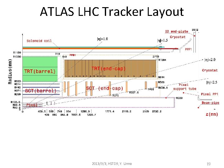
ATLAS LHC Tracker Layout 2013/9/3, HSTD 9, Y. Unno 23