Lecture 11 Microstrip and Array Antennas Microstrip Antennas






- Slides: 62

Lecture 11 Microstrip and Array Antennas ØMicrostrip Antennas ØArray Antennas ØUnderground Radar ØMagnetron ØKlystron ØBackward-Wave Tubes (BWT)

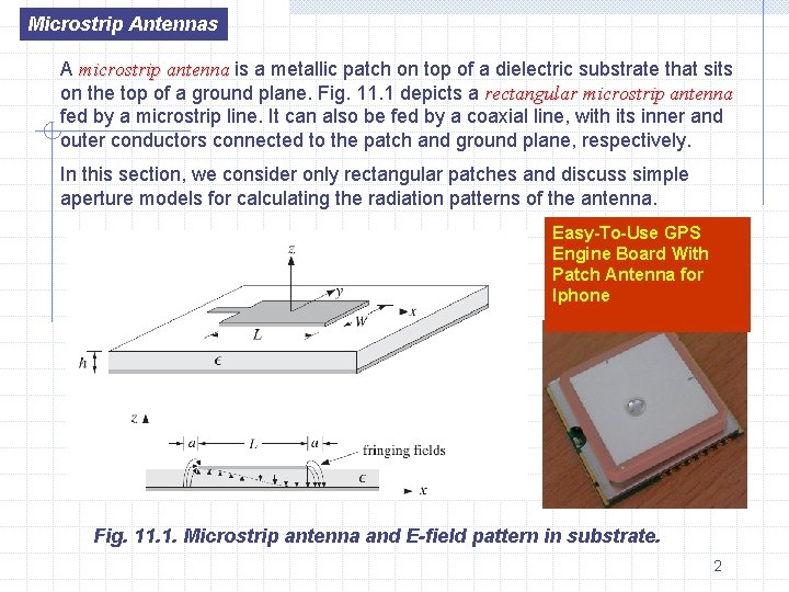
Microstrip Antennas A microstrip antenna is a metallic patch on top of a dielectric substrate that sits on the top of a ground plane. Fig. 11. 1 depicts a rectangular microstrip antenna fed by a microstrip line. It can also be fed by a coaxial line, with its inner and outer conductors connected to the patch and ground plane, respectively. In this section, we consider only rectangular patches and discuss simple aperture models for calculating the radiation patterns of the antenna. Easy-To-Use GPS Engine Board With Patch Antenna for Iphone Fig. 11. 1. Microstrip antenna and E-field pattern in substrate. 2

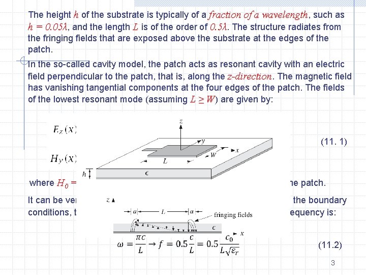
The height h of the substrate is typically of a fraction of a wavelength, such as h = 0. 05λ, and the length L is of the order of 0. 5λ. The structure radiates from the fringing fields that are exposed above the substrate at the edges of the patch. In the so-called cavity model, the patch acts as resonant cavity with an electric field perpendicular to the patch, that is, along the z-direction. The magnetic field has vanishing tangential components at the four edges of the patch. The fields of the lowest resonant mode (assuming L ≥ W) are given by: (11. 1) where H 0 = −j. E 0/Z. We have placed the origin at the middle of the patch. It can be verified that Eqs. (11. 1) satisfy Maxwell’s equations and the boundary conditions, that is, Hy(x)= 0 at x = ±L/2, provided the resonant frequency is: (11. 2) 3

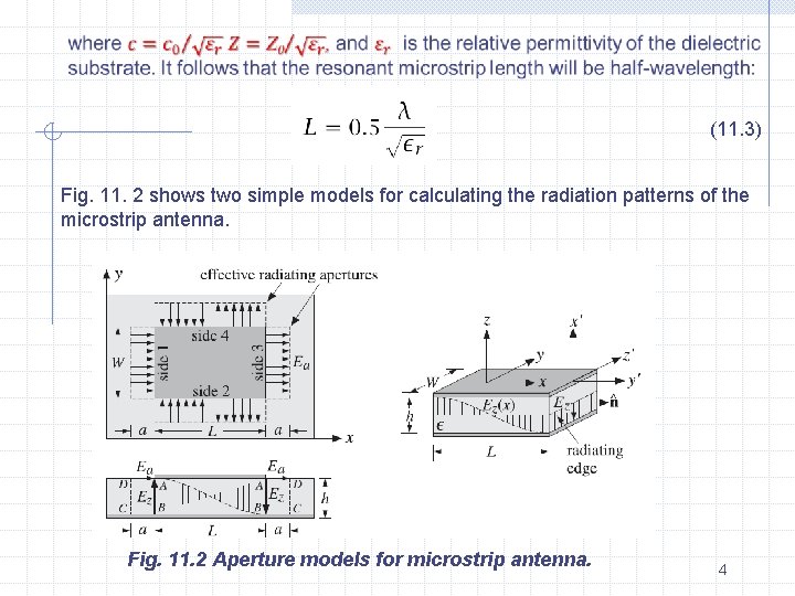
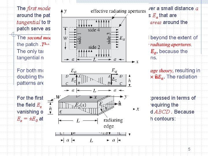
(11. 3) Fig. 11. 2 shows two simple models for calculating the radiation patterns of the microstrip antenna. Fig. 11. 2 Aperture models for microstrip antenna. 4

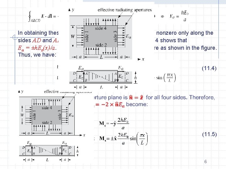
The first model assumes that the fringing fields extend over a small distance a around the patch sides and can be replaced with the fields Ea that are tangential to the substrate surface. The four extended edge areas around the patch serve as the effective radiating apertures For the first model, the effective tangential fields can be expressed in terms of the field Ez by the relationship: a. Ea = h. Ez. This follows by requiring the vanishing of the line integrals of E around the loops labeled ABCD. Because Ez = ±E 0 at x = ±L/2, we obtain from the left and right such contours: 5

In obtaining these, we assumed that the electric field is nonzero only along the sides AD and AB. A similar argument for the sides 2 & 4 shows that Ea = ±h. Ez(x)/a. The directions of Ea at the four sides are as shown in the figure. Thus, we have: (11. 4) (11. 5) 6

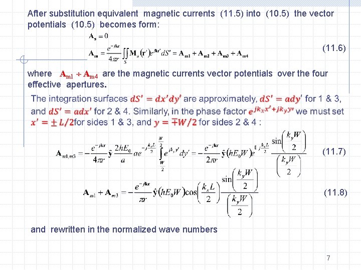
After substitution equivalent magnetic currents (11. 5) into (10. 5) the vector potentials (10. 5) becomes form: (11. 6) where Am 1 Am 4 are the magnetic currents vector potentials over the four effective apertures. (11. 7) (11. 8) and rewritten in the normalized wave numbers 7

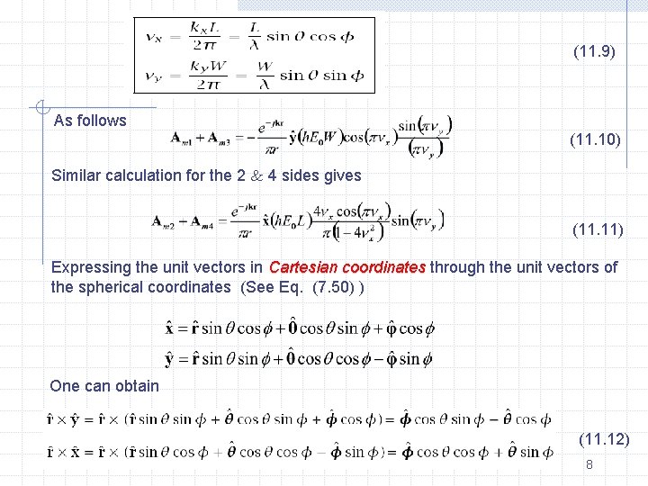
(11. 9) As follows (11. 10) Similar calculation for the 2 4 sides gives (11. 11) Expressing the unit vectors in Cartesian coordinates through the unit vectors of the spherical coordinates (See Eq. (7. 50) ) One can obtain (11. 12) 8

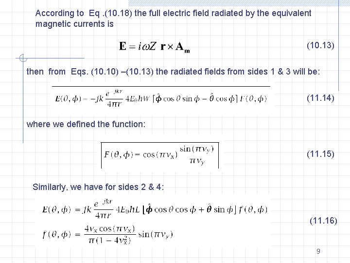
According to Eq. (10. 18) the full electric field radiated by the equivalent magnetic currents is (10. 13) then from Eqs. (10. 10) –(10. 13) the radiated fields from sides 1 & 3 will be: (11. 14) where we defined the function: (11. 15) Similarly, we have for sides 2 & 4: (11. 16) 9

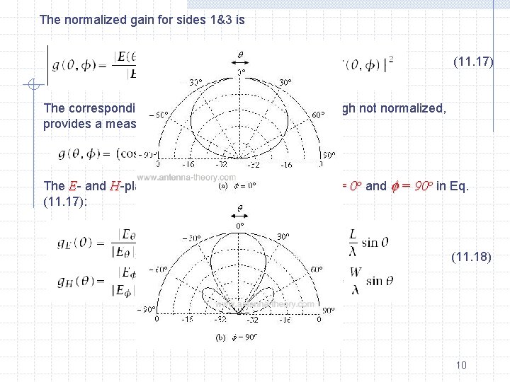
The normalized gain for sides 1&3 is (11. 17) The corresponding expression for sides 2 & 4, although not normalized, provides a measure for the gain in that case: The E- and H-plane gains are obtained by setting = 0 o and = 90 o in Eq. (11. 17): (11. 18) 10

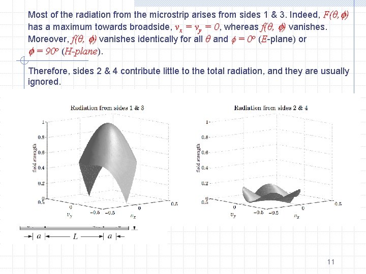
Most of the radiation from the microstrip arises from sides 1 & 3. Indeed, F(θ, ) has a maximum towards broadside, vx = vy = 0, whereas f(θ, ) vanishes. Moreover, f(θ, ) vanishes identically for all θ and = 0 o (E-plane) or = 90 o (H-plane). Therefore, sides 2 & 4 contribute little to the total radiation, and they are usually ignored. 11

12

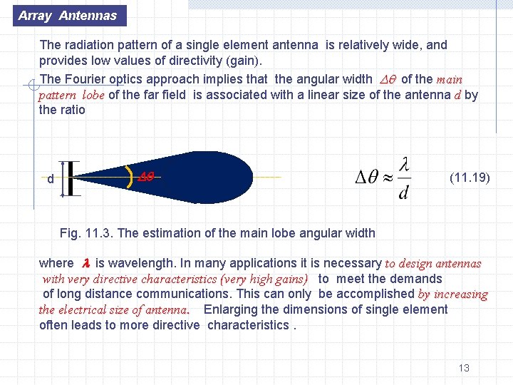
Array Antennas The radiation pattern of a single element antenna is relatively wide, and provides low values of directivity (gain). The Fourier optics approach implies that the angular width of the main pattern lobe of the far field is associated with a linear size of the antenna d by the ratio d (11. 19) Fig. 11. 3. The estimation of the main lobe angular width where is wavelength. In many applications it is necessary to design antennas with very directive characteristics (very high gains) to meet the demands of long distance communications. This can only be accomplished by increasing the electrical size of antenna. Enlarging the dimensions of single element often leads to more directive characteristics. 13

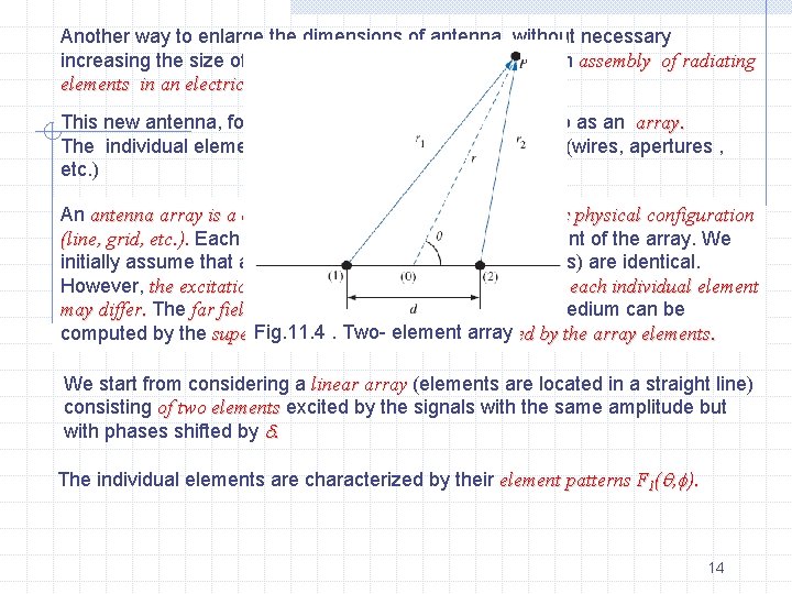
Another way to enlarge the dimensions of antenna, without necessary increasing the size of the individual elements, is to form an assembly of radiating elements in an electrical and geometrical configuration. This new antenna, formed by multi elements, is referred to as an array. The individual elements of an array may be of any form (wires, apertures , etc. ) An antenna array is a cluster of antennas arranged in a specific physical configuration (line, grid, etc. ). Each individual antenna is called an element of the array. We initially assume that all array elements (individual antennas) are identical. However, the excitation (both amplitude and phase) applied to each individual element may differ. The far field radiation from the array in a linear medium can be Fig. 11. 4 of. Twoelement array by the array elements. computed by the superposition the EM fields generated We start from considering a linear array (elements are located in a straight line) consisting of two elements excited by the signals with the same amplitude but with phases shifted by . The individual elements are characterized by their element patterns F 1( , ). 14

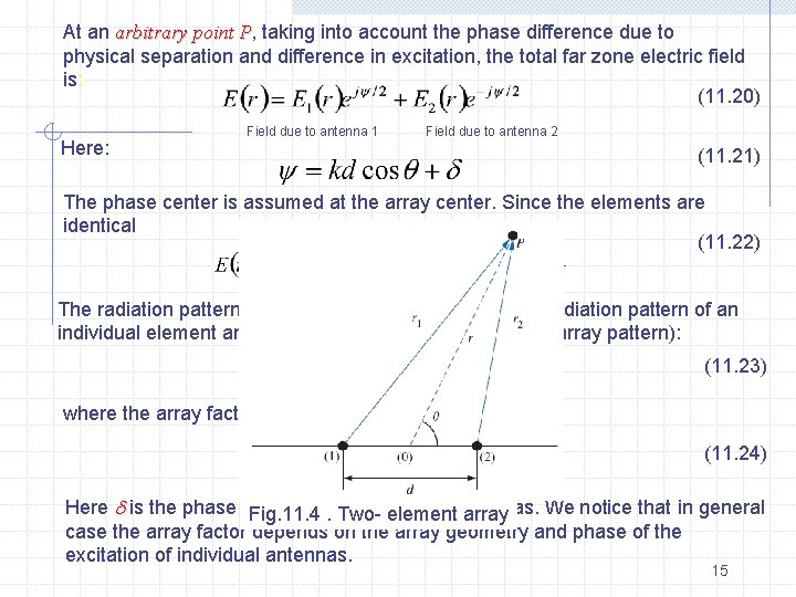
At an arbitrary point P, P taking into account the phase difference due to physical separation and difference in excitation, the total far zone electric field is: (11. 20) Here: Field due to antenna 1 Field due to antenna 2 (11. 21) The phase center is assumed at the array center. Since the elements are identical (11. 22) The radiation pattern can be written as a product of the radiation pattern of an individual element and the radiation pattern of the array (array pattern): (11. 23) where the array factor is: (11. 24) Here is the phase difference two antennas. We notice that in general Fig. 11. 4. between Two- element array case the array factor depends on the array geometry and phase of the excitation of individual antennas. 15

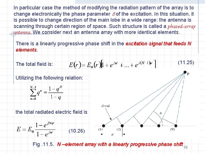
In particular case the method of modifying the radiation pattern of the array is to change electronically the phase parameter of the excitation. In this situation, it is possible to change direction of the main lobe in a wide range: the antenna is scanning through certain region of space. Such structure is called a phased-array antenna. We consider next an antenna array with more identical elements. There is a linearly progressive phase shift in the excitation signal that feeds N elements. (11. 25) The total field is: Utilizing the following relation: the total radiated electric field is (10. 26) Fig. 11. 5. N –element array with a linearly progressive phase shift 16

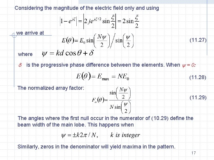
Considering the magnitude of the electric field only and using we arrive at (11. 27) where is the progressive phase difference between the elements. When = 0: (11. 28) The normalized array factor: (11. 29) The angles where the first null occur in the numerator of (10. 29) define the beam width of the main lobe. This happens when Similarly, zeros in the denominator will yield maxima in the pattern. 17

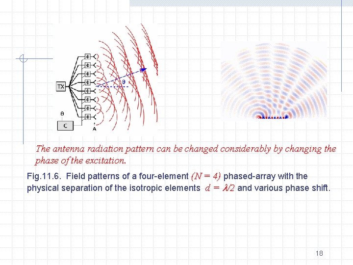
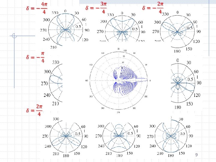
The antenna radiation pattern can be changed considerably by changing the phase of the excitation. Fig. 11. 6. Field patterns of a four-element (N = 4) phased-array with the physical separation of the isotropic elements d = /2 and various phase shift. 18

19

20

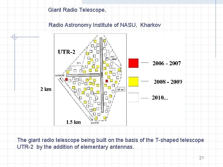
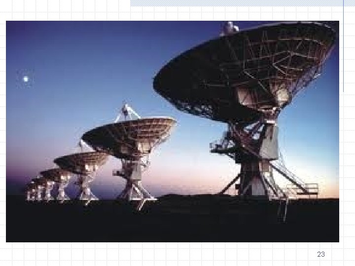
Giant Radio Telescope, Radio Astronomy Institute of NASU, Kharkov The giant radio telescope being built on the basis of the T-shaped telescope UTR-2 by the addition of elementary antennas. 21

1 km • N= 2040 • Effective area 150000 м 2 • Frequency band 8 -35 МHz; • . = 0. 5° • Low back lobes • electronic control of the lobe on both angles coordinates 2 km 22

23

Ground Penetrating Radar for Subsurface Non-invasive Examination (Gaza Tunnel Location)

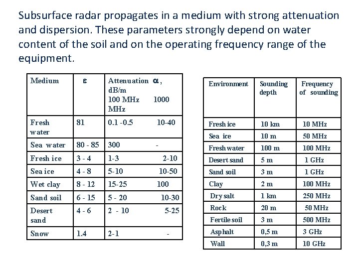
Subsurface radar propagates in a medium with strong attenuation and dispersion. These parameters strongly depend on water content of the soil and on the operating frequency range of the equipment. Medium Attenuation , d. B/m 100 MHz 1000 MHz 0. 1 -0. 5 Sounding depth Frequency of sounding Fresh ice 10 km 10 MHz Sea ice 10 m 50 MHz Fresh water 100 m 100 MHz Desert sand 5 m 1 GHz Fresh water 81 Sea water 80 - 85 300 Fresh ice 3 -4 1 -3 2 -10 Sea ice 4 -8 5 -10 10 -50 Sand soil 3 m 1 GHz Wet clay 8 - 12 15 -25 100 Clay 2 m 100 MHz Sand soil 6 - 15 5 - 20 10 -30 Dry salt 1 km 250 MHz Desert sand 4 -6 2 - 10 5 -25 Rock 20 m 50 MHz Fertile soil 3 m 500 MHz Snow 1. 4 Asphalt 0, 5 m 3 GHz Wall 0, 3 m 10 GHz 2 -1 10 -40 Environment - -

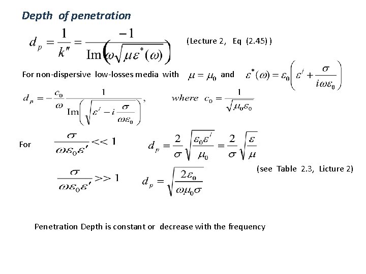
Depth of penetration (Lecture 2, Eq (2. 45) ) For non-dispersive low-losses media with and For (see Table 2. 3, Licture 2) Penetration Depth is constant or decrease with the frequency

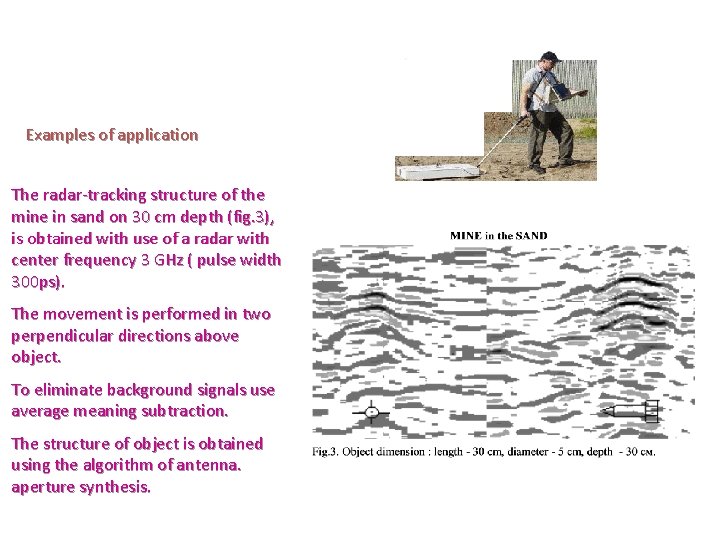
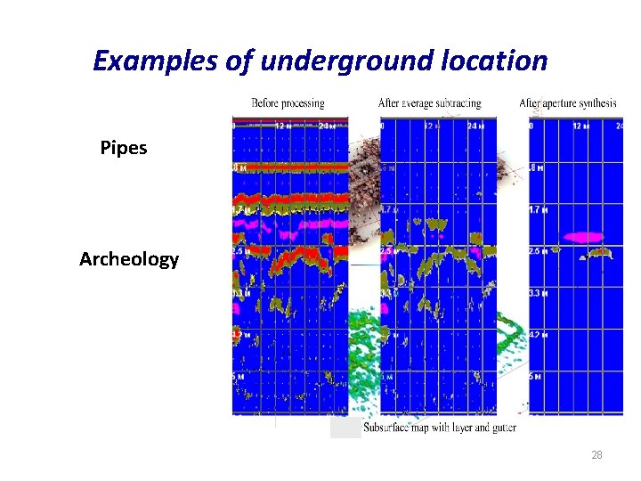
Examples of application The radar-tracking structure of the mine in sand on 30 cm depth (fig. 3), is obtained with use of a radar with center frequency 3 GHz ( pulse width 300 ps). The movement is performed in two perpendicular directions above object. To eliminate background signals use average meaning subtraction. The structure of object is obtained using the algorithm of antenna. aperture synthesis.

Examples of underground location Pipes Archeology 28

Antenna assembly аb-250 Shielded demountable antenna assembly. Central frequency 250 MHz Penetration depth 8 m. Resolution 0, 25 m. Dimensions 1100 х430 х130 (mm). Weight 10 Kg. Power consumption 7, 0 W Antenna assembly AB-150 Shielded demountable antenna assembly. Central frequency 150 MHz Penetration depth 12 m. Resolution 0, 35 m. Dimensions 1600 х620 х170 (mm). Weight 18 Kg. Power consumption 7, 0 W Antenna assembly AB-90 Shielded demountable antenna assembly. Central frequency 90 MHz Penetration depth 16 m. Resolution 0, 5 m. Dimensions 2220 х1000 х270(mm). Weight 37 Kg. Power consumption 8, 0 W Antenna assembly AB-250 Unshielded demountable antenna assembly. Central frequency 50 -100 MHz Penetration depth up to 20 m. Resolution from 0. 5 up to 2. 0 m Plug-in dipole radiators from 50 up to 100 MHz. Dimensions 1100 х430 х130 (mm). Weight 6 Kg. Power consumption 8, 0 W

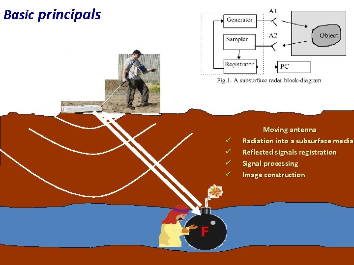
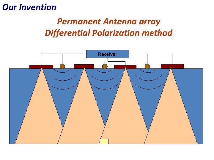
Basic principals ü ü Moving antenna Radiation into a subsurface media Reflected signals registration Signal processing Image construction 30

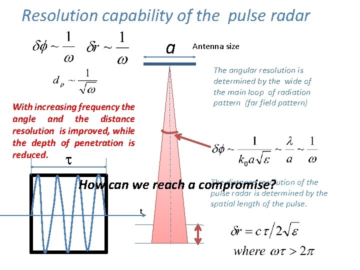
Resolution capability of the pulse radar a Antenna size The angular resolution is determined by the wide of the main loop of radiation pattern (far field pattern) With increasing frequency the angle and the distance resolution is improved, while the depth of penetration is reduced. The distance resolution of the How can we reach a compromise? pulse radar is determined by the t spatial length of the pulse.

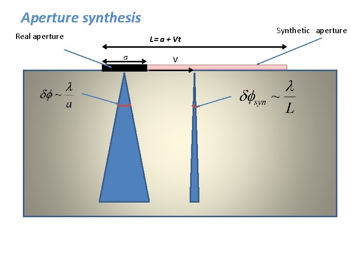
Aperture synthesis Real aperture L= a + Vt a V Synthetic aperture

Our Invention Permanent Antenna array Differential Polarization method Receiver

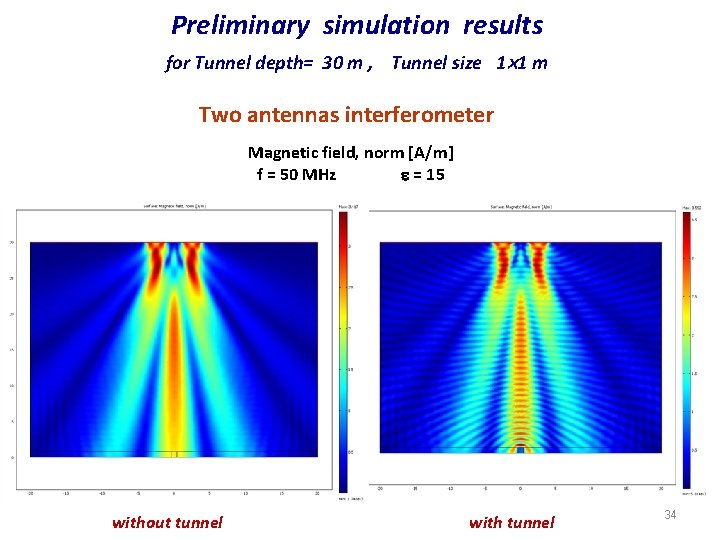
Preliminary simulation results for Tunnel depth= 30 m , Tunnel size 1 1 m Two antennas interferometer Magnetic field, norm [A/m] f = 50 MHz = 15 without tunnel with tunnel 34

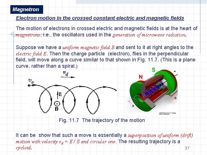
Magnetron Electron motion in the crossed constant electric and magnetic fields The motion of electrons in crossed electric and magnetic fields is at the heart of magnetrons, magnetrons i. e. , the oscillators used in the generation of microwave radiation Suppose we have a uniform magnetic field B and sent to it at right angles to the electric field E. E Then the charge particle (electron), flies in the perpendicular field, will move along a curve similar to that shown in Fig. 11. 7. (This is a plane curve, rather than a spiral. ) Fig. 11. 7 The trajectory of the motion It can be show that such a move is essentially a superposition of uniform (drift) motion with velocity vd = E / B and circular one The resulting trajectory is a cycloid. 37

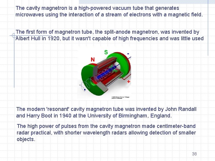
The cavity magnetron is a high-powered vacuum tube that generates microwaves using the interaction of a stream of electrons with a magnetic field. The first form of magnetron tube, the split-anode magnetron, was invented by Albert Hull in 1920, but it wasn't capable of high frequencies and was little used The modern 'resonant' cavity magnetron tube was invented by John Randall and Harry Boot in 1940 at the University of Birmingham, England. The high power of pulses from the cavity magnetron made centimeter-band radar practical, with shorter wavelength radars allowing detection of smaller objects. 38

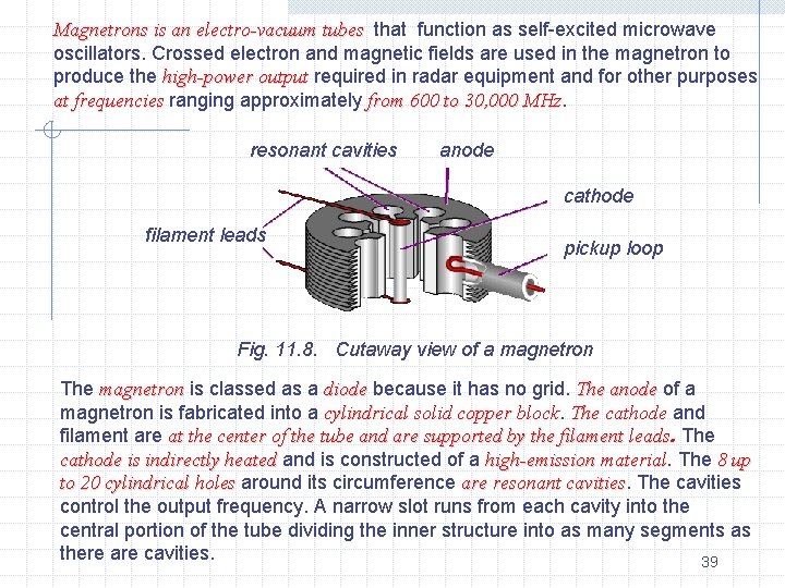
Magnetrons is an electro-vacuum tubes that function as self-excited microwave oscillators. Crossed electron and magnetic fields are used in the magnetron to produce the high-power output required in radar equipment and for other purposes at frequencies ranging approximately from 600 to 30, 000 MHz resonant cavities anode cathode filament leads pickup loop Fig. 11. 8. Cutaway view of a magnetron The magnetron is classed as a diode because it has no grid. The anode of a magnetron is fabricated into a cylindrical solid copper block The cathode and filament are at the center of the tube and are supported by the filament leads The cathode is indirectly heated and is constructed of a high-emission material The 8 up to 20 cylindrical holes around its circumference are resonant cavities The cavities control the output frequency. A narrow slot runs from each cavity into the central portion of the tube dividing the inner structure into as many segments as there are cavities. 39

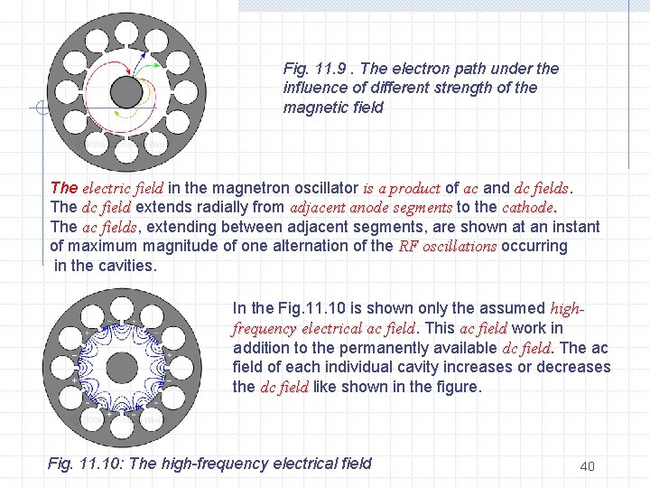
Fig. 11. 9. The electron path under the influence of different strength of the magnetic field The electric field in the magnetron oscillator is a product of ac and dc fields The dc field extends radially from adjacent anode segments to the cathode. The ac fields, fields extending between adjacent segments, are shown at an instant of maximum magnitude of one alternation of the RF oscillations occurring in the cavities. In the Fig. 11. 10 is shown only the assumed highfrequency electrical ac field This ac field work in addition to the permanently available dc field. The ac field of each individual cavity increases or decreases the dc field like shown in the figure. Fig. 11. 10: The high-frequency electrical field 40

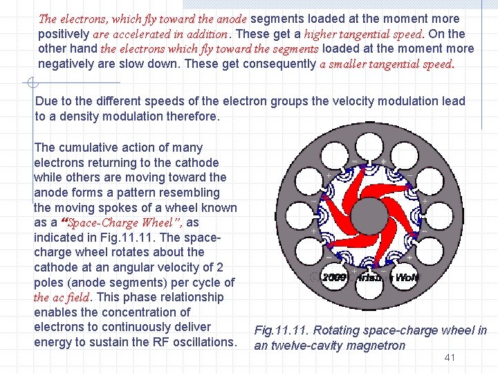
The electrons, which fly toward the anode segments loaded at the moment more positively are accelerated in addition These get a higher tangential speed. On the other hand the electrons which fly toward the segments loaded at the moment more negatively are slow down. These get consequently a smaller tangential speed. Due to the different speeds of the electron groups the velocity modulation lead to a density modulation therefore. The cumulative action of many electrons returning to the cathode while others are moving toward the anode forms a pattern resembling the moving spokes of a wheel known as a “Space-Charge Wheel”, as indicated in Fig. 11. The spacecharge wheel rotates about the cathode at an angular velocity of 2 poles (anode segments) per cycle of the ac field This phase relationship enables the concentration of electrons to continuously deliver energy to sustain the RF oscillations. Fig. 11. Rotating space-charge wheel in an twelve-cavity magnetron 41

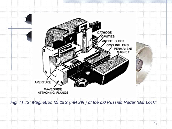
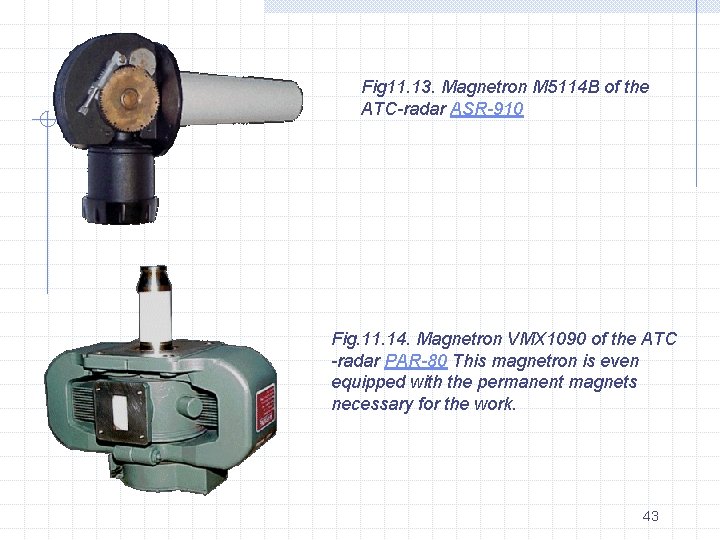
Fig. 11. 12: Magnetron MI 29 G (МИ 29 Г) of the old Russian Radar “Bar Lock” 42

Fig 11. 13. Magnetron M 5114 B of the ATC-radar ASR-910 Fig. 11. 14. Magnetron VMX 1090 of the ATC -radar PAR-80 This magnetron is even equipped with the permanent magnets necessary for the work. 43

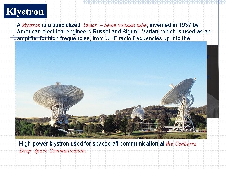
Klystron A klystron is a specialized linear – beam vacuum tube, tube invented in 1937 by American electrical engineers Russel and Sigurd Varian, which is used as an amplifier for high frequencies, from UHF radio frequencies up into the microwave range. Low-power klystrons are used as local oscillators in supergetertodyne radar receivers, while high-power klystrons are used as output tubes in UHF television transmitters, microwave relay, satellite communication, and radar transmitters, and to generate the drive power for modern particle accelerator. Klystron amplifiers have the advantage (over the magnetron) of coherently amplifying a reference signal so its output may be precisely controlled in amplitude, frequency and phase. The name klystron comes from the stem form κλυσ- (klys) of a Greek verb referring to the action of waves breaking against a shore, and the end of the word electron. High-power klystron used for spacecraft communication at the Canberra Deep Space Communication.

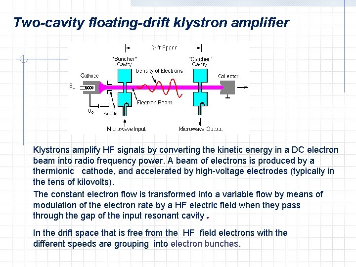
Two-cavity floating-drift klystron amplifier Klystrons amplify HF signals by converting the kinetic energy in a DC electron beam into radio frequency power. A beam of electrons is produced by a thermionic cathode, and accelerated by high-voltage electrodes (typically in the tens of kilovolts). The constant electron flow is transformed into a variable flow by means of modulation of the electron rate by a HF electric field when they pass through the gap of the input resonant cavity. In the drift space that is free from the HF field electrons with the different speeds are grouping into electron bunches.

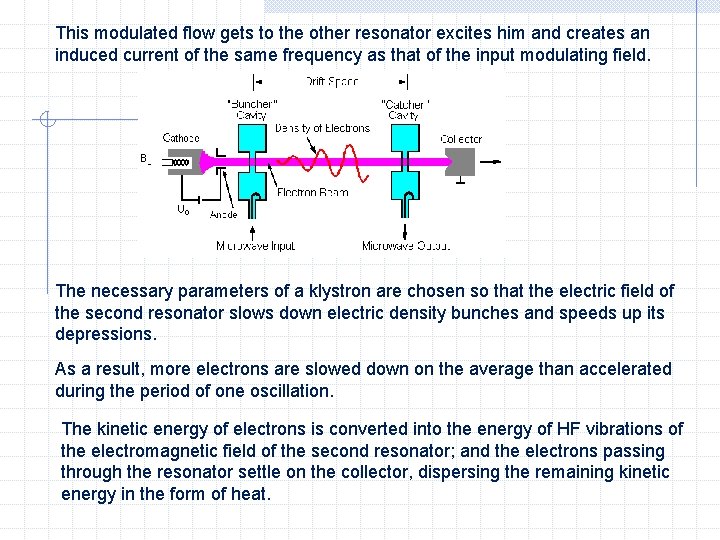
This modulated flow gets to the other resonator excites him and creates an induced current of the same frequency as that of the input modulating field. The necessary parameters of a klystron are chosen so that the electric field of the second resonator slows down electric density bunches and speeds up its depressions. As a result, more electrons are slowed down on the average than accelerated during the period of one oscillation. The kinetic energy of electrons is converted into the energy of HF vibrations of the electromagnetic field of the second resonator; and the electrons passing through the resonator settle on the collector, dispersing the remaining kinetic energy in the form of heat.

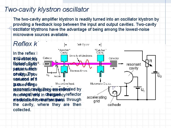
Two-cavity klystron oscillator The two-cavity amplifier klystron is readily turned into an oscillator klystron by providing a feedback loop between the input and output cavities. Two-cavity oscillator klystrons have the advantage of being among the lowest-noise microwave sources available. Reflex klystron In the reflex klystron (also known as a 'Sutton' klystron after itsbe inventor, The reflector voltage may Robert Sutton), thethe electron beam varied slightly from optimum passes through a single value, which results in someresonant loss cavity. The electrons areinfired of output power, but also a into one end in of frequency. the tube by. This an effect electron variation gun. passing through is used. After to good advantage for the resonant they are reflected by automaticcavity frequency control in a negatively receivers, and in charged frequency reflector electrode for pass through modulation foranother transmitters. the cavity, where they are then collected.

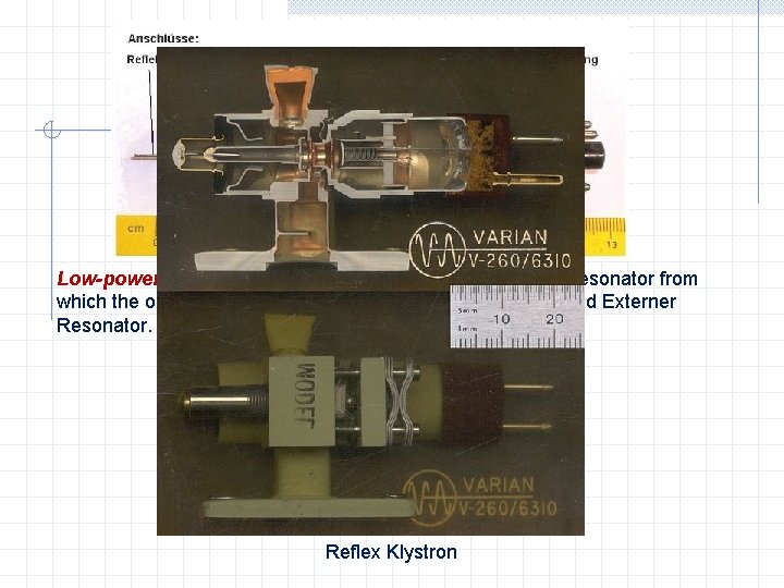
Low-power Russian reflex klystron from 1963. The cavity resonator from which the output is taken, is attached to the electrodes labeled Externer Resonator. Reflex Klystron

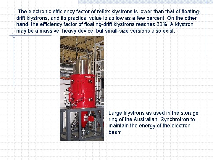
The electronic efficiency factor of reflex klystrons is lower than that of floatingdrift klystrons, and its practical value is as low as a few percent. On the other hand, the efficiency factor of floating-drift klystrons reaches 58%. A klystron may be a massive, heavy device, but small-size versions also exist. Large klystrons as used in the storage ring of the Australian Synchrotron to maintain the energy of the electron beam

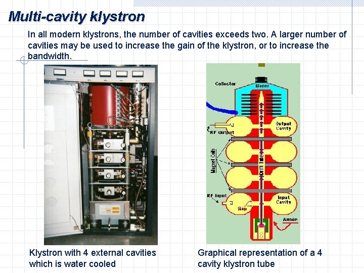
Multi-cavity klystron In all modern klystrons, the number of cavities exceeds two. A larger number of cavities may be used to increase the gain of the klystron, or to increase the bandwidth. Klystron with 4 external cavities which is water cooled Graphical representation of a 4 cavity klystron tube

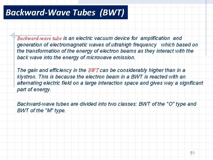
Backward-Wave Tubes (BWT) Backward-wave tube is an electric vacuum device for amplification and generation of electromagnetic waves of ultrahigh frequency which based on the transformation of the energy of electron beams as they interact with the back wave into the energy of microwave emission. The gain and efficiency in the BWT can be considerably higher than in a klystron. This is because the electron beam in a BWT is reacted with an alternating electric field on a large interaction space and gives way a significant part of energy. Backward-wave tubes are divided into two classes: BWT of the "O" type and BWT of the "M" type. 51

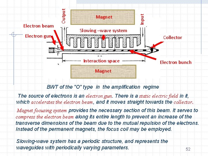
Electron gun Input Output Electron beam Magnet Slowing –wave system Collector Interaction space Electron bunch Magnet BWT of the "O" type in the amplification regime The source of electrons is an electron gun There is a static electric field in it, which accelerates the electron beam, beam and it moves straight towards the collector. Magnet focusing system provides the necessary section of this beam. It serves to compress the electron beam along its entire length to prevent an increase of the transverse dimensions of the beam due to the mutual repulsion of the electrons. Instead of the permanent magnets, the focus coil may be employed. Slowing-wave system has a periodic structure, and represents the waveguides with periodically varying parameters. 52

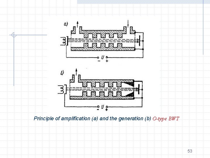
Principle of amplification (a) and the generation (b) O-type BWT 53

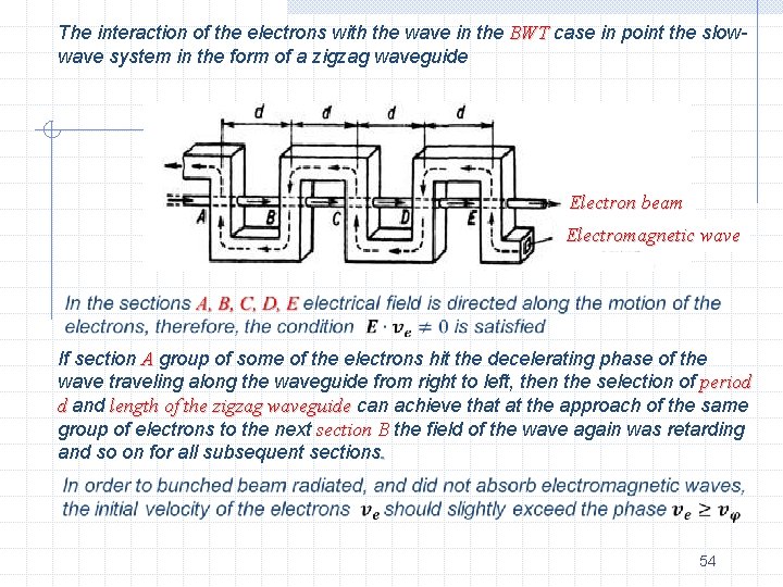
The interaction of the electrons with the wave in the BWT case in point the slowwave system in the form of a zigzag waveguide Electron beam Electromagnetic wave If section A group of some of the electrons hit the decelerating phase of the wave traveling along the waveguide from right to left, then the selection of period d and length of the zigzag waveguide can achieve that at the approach of the same group of electrons to the next section B the field of the wave again was retarding and so on for all subsequent sections. 54

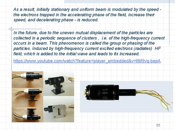
As a result, initially stationary and uniform beam is modulated by the speed the electrons trapped in the accelerating phase of the field, increase their speed, and decelerating phase - is reduced. In the future, due to the uneven mutual displacement of the particles are collected in a periodic sequence of clusters , i. e. of the high-frequency current occurs in a beam. This phenomenon is called the group or phasing of the particles. Induced by high-frequency current excited electrons (radiates) HF field, which is added to the initial wave and leads to its increased. https: //www. youtube. com/watch? feature=player_embedded&v=tl. M 9 vq-bep. A 55

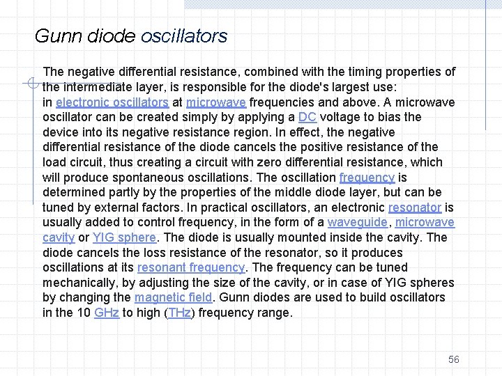
Gunn diode oscillators The negative differential resistance, combined with the timing properties of the intermediate layer, is responsible for the diode's largest use: in electronic oscillators at microwave frequencies and above. A microwave oscillator can be created simply by applying a DC voltage to bias the device into its negative resistance region. In effect, the negative differential resistance of the diode cancels the positive resistance of the load circuit, thus creating a circuit with zero differential resistance, which will produce spontaneous oscillations. The oscillation frequency is determined partly by the properties of the middle diode layer, but can be tuned by external factors. In practical oscillators, an electronic resonator is usually added to control frequency, in the form of a waveguide, microwave cavity or YIG sphere. The diode is usually mounted inside the cavity. The diode cancels the loss resistance of the resonator, so it produces oscillations at its resonant frequency. The frequency can be tuned mechanically, by adjusting the size of the cavity, or in case of YIG spheres by changing the magnetic field. Gunn diodes are used to build oscillators in the 10 GHz to high (THz) frequency range. 56

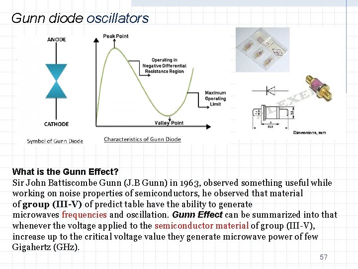
Gunn diode oscillators What is the Gunn Effect? Sir John Battiscombe Gunn (J. B Gunn) in 1963, observed something useful while working on noise properties of semiconductors, he observed that material of group (III-V) of predict table have the ability to generate microwaves frequencies and oscillation. Gunn Effect can be summarized into that whenever the voltage applied to the semiconductor material of group (III-V), increase up to the critical voltage value they generate microwave power of few Gigahertz (GHz). 57

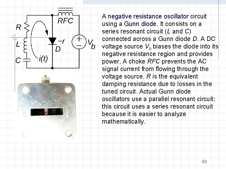
A negative resistance oscillator circuit using a Gunn diode. It consists on a series resonant circuit (L and C) connected across a Gunn diode D. A DC voltage source Vb biases the diode into its negative resistance region and provides power. A choke RFC prevents the AC signal current from flowing through the voltage source. R is the equivalent damping resistance due to losses in the tuned circuit. Actual Gunn diode oscillators use a parallel resonant circuit; this circuit uses a series resonant circuit because it is easier to analyze mathematically. 58

59

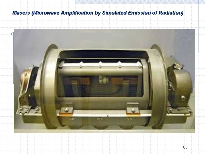
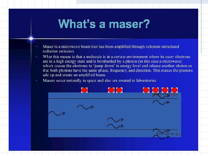
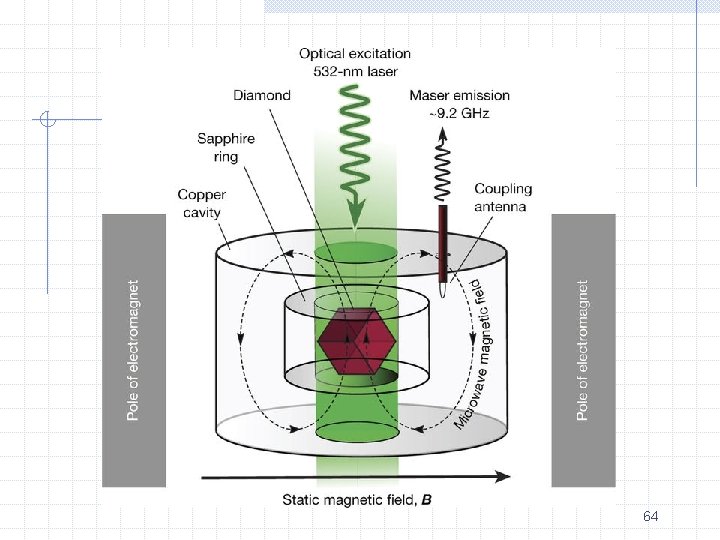
Masers (Microwave Amplification by Simulated Emission of Radiation) 60

61

62

63

64