Development of Silicon Microstrip Sensors in 150 mm
- Slides: 18

Development of Silicon Microstrip Sensors in 150 mm p-type Wafers Y. Unno, S. Terada, Y. Ikegami, T. Kohriki, K. Hara, and the ATLAS R&D collaboration of "Development of noninverting Silicon strip detectors for the ATLAS ID upgrade" K. Yamamura, S. Kamada (Hamamatsu Photonics) Y. Unno, 3 rd Workshop on Advanced Silicon Radiation Detectors, Barcelona, Spain, 14 -16 April. 2008

Some History of Development • 1995 p-type 4 -inch (100 mm) wafer (p 95) – FZ(111) (~6 kΩcm) wafers • 2005 p-type 4 -inch (100 mm) wafer (ATLAS 05) – FZ(111) (~6 k Ωcm) – MCZ(100) (~900 Ωcm) wafers • 2006 p-type 6 -inch (150 mm) wafer (ATLAS 06) – FZ-1(100)(~6. 7 k Ωcm), FZ-2(100)(~6. 2 k Ωcm) – MCZ(100)(~2. 3 k Ωcm) • 2007 p-type 6 -inch (150 mm) wafer (ATLAS 07) – FZ-1(100)(~6. 7 k Ωcm), FZ-2(100)(~6. 2 k Ωcm) Y. Unno, 3 rd Workshop on Advanced Silicon Radiation Detectors, Barcelona, Spain, 14 -16 April. 2008

p 95 p-type Sensors • A prototype n-in-p sensor was fabricated in 1995 – 6 cm x 300 um, 50 um pitch, common p-stop • no DC-field plate over p-stop – p-bulk, (111), ~6 kΩcm – Irradiated up to 1. 1 x 10¹⁴ p/cm 2 at 12 Ge. V PS at KEK – A report was made in NIM A 383(96)159 – Re-measurements after 10 yrs (irrad. stored at 0 C) • I-V • CCE with laser Y. Unno, 3 rd Workshop on Advanced Silicon Radiation Detectors, Barcelona, Spain, 14 -16 April. 2008

ATLAS 05 p-type Sensors • Investigation of isolation of n-strips – p-stop with/without p-spray – With/without field-plate – p-stop doping levels Y. Unno, 3 rd Workshop on Advanced Silicon Radiation Detectors, Barcelona, Spain, 14 -16 April. 2008

ATLAS 05 p-type Sensors • p-type wafers – 4 -inch wafer for cost reason – MCZ: • ~900 Ωcm • Orientation (100) – FZ: • ~6 k Ωcm • Orientation (111) • Sensors – Miniature: 1 cm x 1 cm – Large: ((~1 cm x ~6 cm) x 6 zones) Y. Unno, 3 rd Workshop on Advanced Silicon Radiation Detectors, Barcelona, Spain, 14 -16 April. 2008

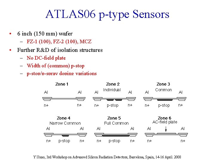
ATLAS 06 p-type Sensors • 6 inch (150 mm) wafer – FZ-1 (100), FZ-2 (100), MCZ • Further R&D of isolation structures – No DC-field plate – Width of (common) p-stop – p-stop/p-spray doping variations Y. Unno, 3 rd Workshop on Advanced Silicon Radiation Detectors, Barcelona, Spain, 14 -16 April. 2008

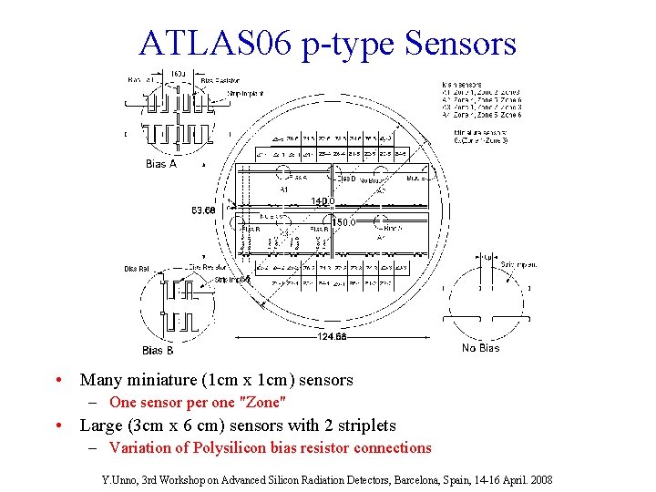
ATLAS 06 p-type Sensors • Many miniature (1 cm x 1 cm) sensors – One sensor per one "Zone" • Large (3 cm x 6 cm) sensors with 2 striplets – Variation of Polysilicon bias resistor connections Y. Unno, 3 rd Workshop on Advanced Silicon Radiation Detectors, Barcelona, Spain, 14 -16 April. 2008

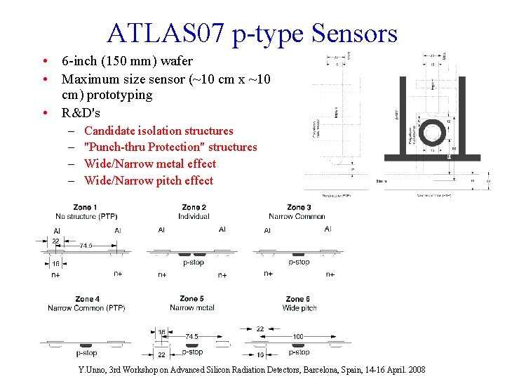
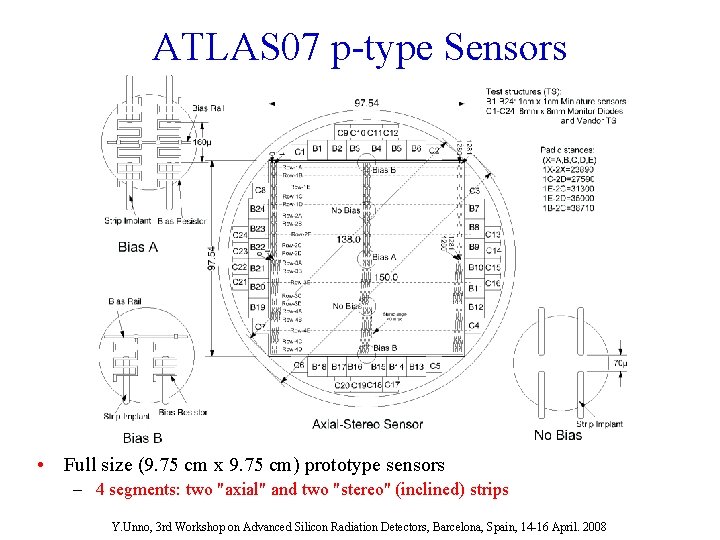
ATLAS 07 p-type Sensors • 6 -inch (150 mm) wafer • Maximum size sensor (~10 cm x ~10 cm) prototyping • R&D's – – Candidate isolation structures "Punch-thru Protection" structures Wide/Narrow metal effect Wide/Narrow pitch effect Y. Unno, 3 rd Workshop on Advanced Silicon Radiation Detectors, Barcelona, Spain, 14 -16 April. 2008

ATLAS 07 p-type Sensors • Full size (9. 75 cm x 9. 75 cm) prototype sensors – 4 segments: two "axial" and two "stereo" (inclined) strips Y. Unno, 3 rd Workshop on Advanced Silicon Radiation Detectors, Barcelona, Spain, 14 -16 April. 2008

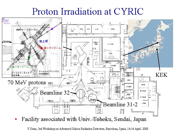
Proton Irradiation at CYRIC KEK 70 Me. V protons Beamline 32 Beamline 31 -2 • Facility associated with Univ. Tohoku, Sendai, Japan Y. Unno, 3 rd Workshop on Advanced Silicon Radiation Detectors, Barcelona, Spain, 14 -16 April. 2008

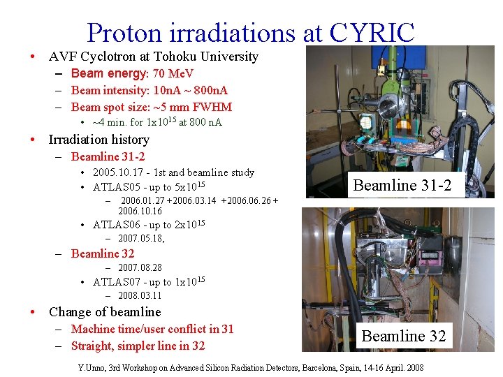
Proton irradiations at CYRIC • AVF Cyclotron at Tohoku University – Beam energy: 70 Me. V – Beam intensity: 10 n. A ~ 800 n. A – Beam spot size: ~5 mm FWHM • ~4 min. for 1 x 10¹⁵ at 800 n. A • Irradiation history – Beamline 31 -2 • 2005. 10. 17 - 1 st and beamline study • ATLAS 05 - up to 5 x 10¹⁵ Beamline 31 -2 – 2006. 01. 27 +2006. 03. 14 +2006. 26 + 2006. 10. 16 • ATLAS 06 - up to 2 x 10¹⁵ – 2007. 05. 18, – Beamline 32 – 2007. 08. 28 • ATLAS 07 - up to 1 x 10¹⁵ – 2008. 03. 11 • Change of beamline – Machine time/user conflict in 31 – Straight, simpler line in 32 Beamline 32 Y. Unno, 3 rd Workshop on Advanced Silicon Radiation Detectors, Barcelona, Spain, 14 -16 April. 2008

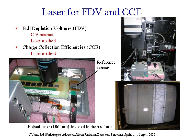
Laser for FDV and CCE • Full Depletion Voltages (FDV) – C-V method – Laser method • Charge Collection Efficiencies (CCE) – Laser method Reference sensor Pulsed laser (1064 nm) focused to 4 um x 4 um Y. Unno, 3 rd Workshop on Advanced Silicon Radiation Detectors, Barcelona, Spain, 14 -16 April. 2008

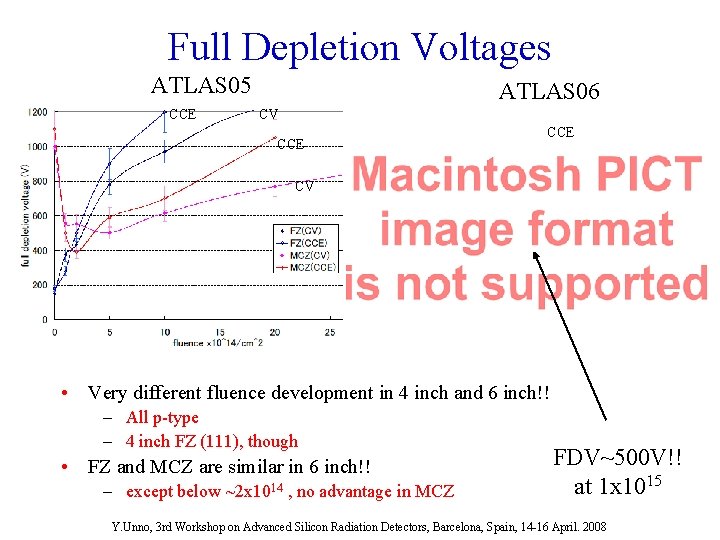
Full Depletion Voltages ATLAS 05 CCE ATLAS 06 CV CCE CV • Very different fluence development in 4 inch and 6 inch!! – All p-type – 4 inch FZ (111), though • FZ and MCZ are similar in 6 inch!! – except below ~2 x 10¹⁴ , no advantage in MCZ FDV~500 V!! at 1 x 10¹⁵ Y. Unno, 3 rd Workshop on Advanced Silicon Radiation Detectors, Barcelona, Spain, 14 -16 April. 2008

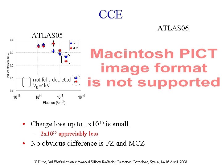
CCE ATLAS 05 ATLAS 06 not fully depleted VB=1 k. V • Charge loss up to 1 x 10¹⁵ is small – 2 x 10¹⁵ appreciably less • No obvious difference is FZ and MCZ Y. Unno, 3 rd Workshop on Advanced Silicon Radiation Detectors, Barcelona, Spain, 14 -16 April. 2008

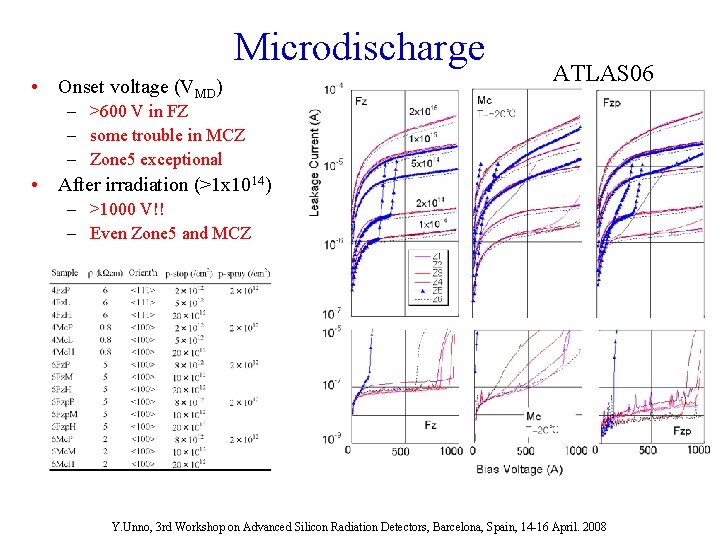
Microdischarge • Onset voltage (VMD) ATLAS 06 – >600 V in FZ – some trouble in MCZ – Zone 5 exceptional • After irradiation (>1 x 10¹⁴) – >1000 V!! – Even Zone 5 and MCZ Y. Unno, 3 rd Workshop on Advanced Silicon Radiation Detectors, Barcelona, Spain, 14 -16 April. 2008

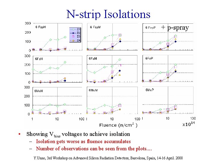
N-strip Isolations + p-spray • Showing Vbias voltages to achieve isolation – Isolation gets worse as fluence accumulates – Number of observations can be seen from the plots. . Y. Unno, 3 rd Workshop on Advanced Silicon Radiation Detectors, Barcelona, Spain, 14 -16 April. 2008

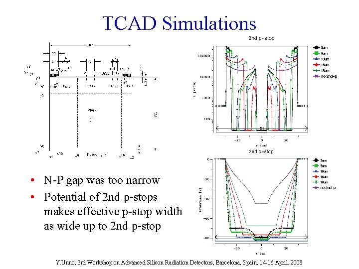
TCAD Simulations • N-P gap was too narrow • Potential of 2 nd p-stops makes effective p-stop width as wide up to 2 nd p-stop Y. Unno, 3 rd Workshop on Advanced Silicon Radiation Detectors, Barcelona, Spain, 14 -16 April. 2008

Summary • n-in-p p-type microstrip sensors have been fabricated in p-FZ and p. MCZ wafers, for several years by now • Proton irradiations, 70 Me. V, are being routinely carried out at CYRIC of Tohoku Univ. , • Fluence development of full depletion voltage (FDV) of 4 -inch (100 mm) and 6 -inch (150 mm) is very different • In 6 -inch, FDV is ~500 V at 1 x 10¹⁵ neq/cm 2 • CCE is near full up to 1 x 10¹⁵ neq/cm 2 • Onset voltage of the microdischarge has been achieved to be >600 V in general • Number of isolation structures are being investigated and we are narrowing the candidates • A full size microstrip sensor has been prototyped and we have the first look in hand Y. Unno, 3 rd Workshop on Advanced Silicon Radiation Detectors, Barcelona, Spain, 14 -16 April. 2008