Design of SMPS Prof V M Aranake Vishwakarma
- Slides: 15

Design of SMPS Prof. V. M. Aranake Vishwakarma Institute of Information Technology Pune-48

Syllabus • General Block diagram of SMPS, Advantages of SMPS, Comparison between SMPS and Linear power supply. • Basic concepts of switching regulators, Basic topologies, Step down converters, step up converters, Flyback converter, Forward converter. • Performance parameters of SMPS • Selection criteria of switching element, switching diode, filter capacitor and inductor. PWM circuit, High frequency transformer design steps. • Protection circuits for SMPS.

Assignments • Paper design should be functionally verified with an appropriate EDA tool and prepare a document consisting • 1. Problem statement 2. Specifications • 3. Block diagram 4. Component Selection • 5. Design calculations 6. simulation results • 7. Bill of material 8. Conclusion • 9. Datasheets 10. Detail circuit diagram

Assignments • Assignment 1: Design and implementation of SMPS • A) Design and simulate buck converter using ICs’ like 3842/3524 and measure performance parameters like load regulation, ripple rejection, output impedance , dropout voltage. • Design and implement buck converter using ICs’ like 3842/3524 and measure performance parameters like load regulation, ripple rejection, output impedance , dropout voltage.

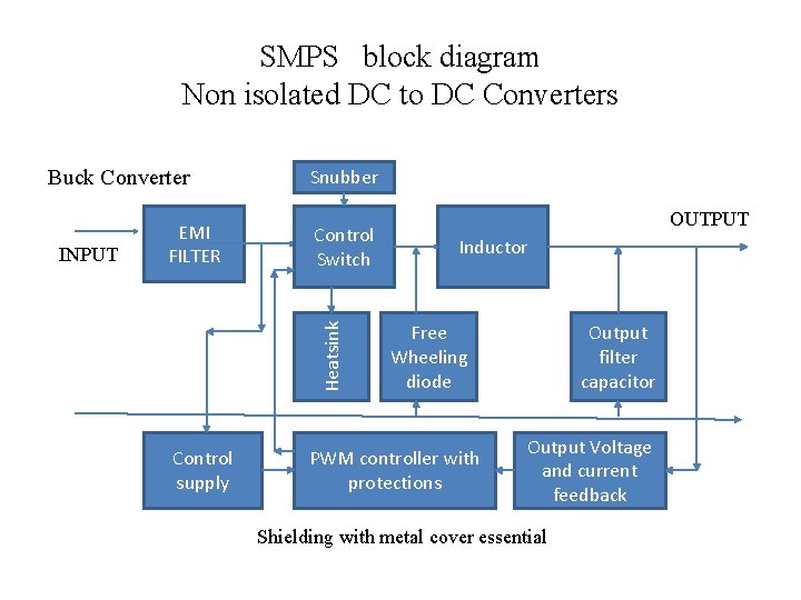
SMPS block diagram Non isolated DC to DC Converters Buck Converter Control Switch Heatsink INPUT EMI FILTER Snubber Control supply OUTPUT Inductor Free Wheeling diode PWM controller with protections Output filter capacitor Output Voltage and current feedback Shielding with metal cover essential

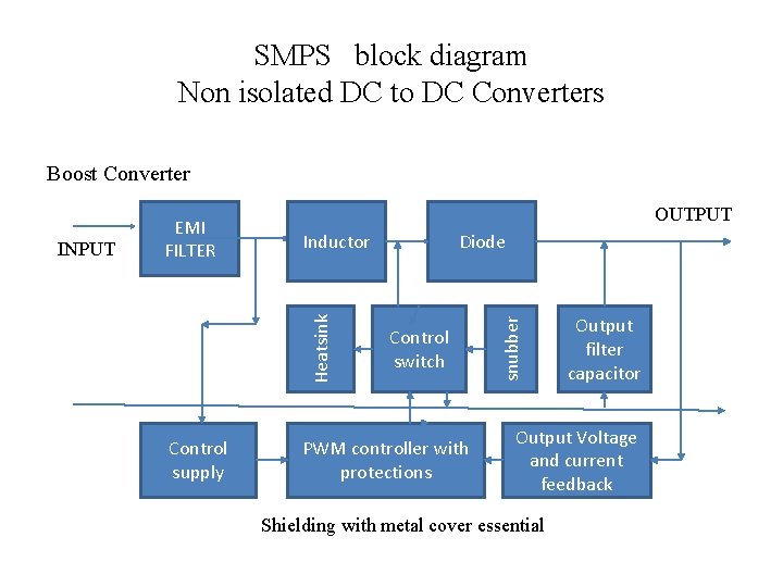
SMPS block diagram Non isolated DC to DC Converters Boost Converter OUTPUT Control supply Diode Control switch PWM controller with protections snubber Inductor Heatsink INPUT EMI FILTER Output filter capacitor Output Voltage and current feedback Shielding with metal cover essential

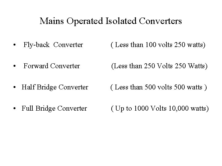
Mains Operated Isolated Converters • Fly-back Converter ( Less than 100 volts 250 watts) • Forward Converter (Less than 250 Volts 250 Watts) • Half Bridge Converter ( Less than 500 volts 500 watts ) • Full Bridge Converter ( Up to 1000 Volts 10, 000 watts)

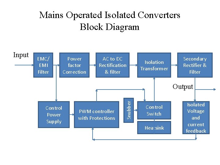
Mains Operated Isolated Converters Block Diagram EMC/ EMI Filter Power factor Correction AC to DC Rectification & filter Isolation Transformer Secondary Rectifier & Filter Output Control Power Supply PWM controller with Protections Snubber Input Control Switch Heatsink Isolated Voltage and current feedback

OPERATING MODES • Continuous Current Mode • Discontinuous Current Mode

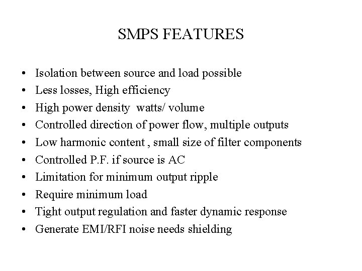
SMPS FEATURES • • • Isolation between source and load possible Less losses, High efficiency High power density watts/ volume Controlled direction of power flow, multiple outputs Low harmonic content , small size of filter components Controlled P. F. if source is AC Limitation for minimum output ripple Require minimum load Tight output regulation and faster dynamic response Generate EMI/RFI noise needs shielding

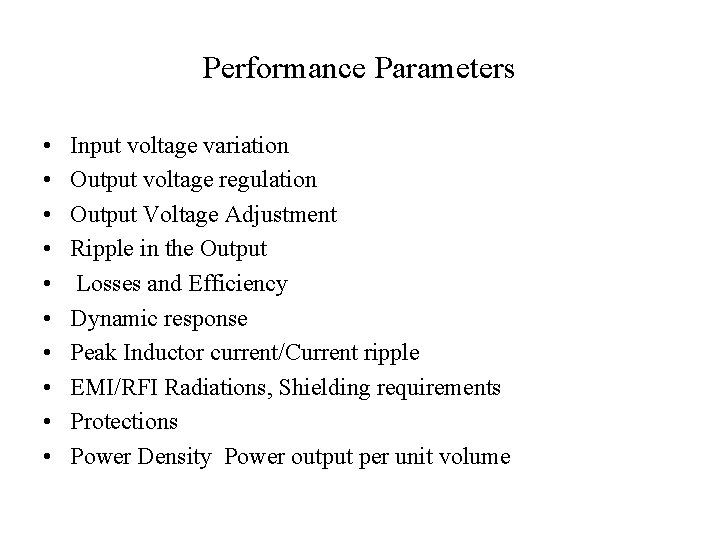
Performance Parameters • • • Input voltage variation Output voltage regulation Output Voltage Adjustment Ripple in the Output Losses and Efficiency Dynamic response Peak Inductor current/Current ripple EMI/RFI Radiations, Shielding requirements Protections Power Density Power output per unit volume

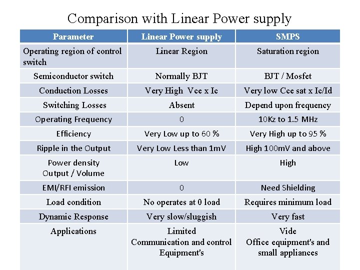
Comparison with Linear Power supply Parameter Linear Power supply SMPS Operating region of control switch Linear Region Saturation region Semiconductor switch Normally BJT / Mosfet Conduction Losses Very High Vce x Ic Very low Cce sat x Ic/Id Switching Losses Absent Depend upon frequency Operating Frequency 0 10 Kz to 1. 5 MHz Efficiency Very Low up to 60 % Very High up to 95 % Ripple in the Output Very Low Less than 1 m. V High 100 m. V and above Power density Output / Volume Low High EMI/RFI emission 0 Need Shielding Load condition No operates at 0 load Requires minimum load Dynamic Response Very slow/sluggish Very fast Applications Limited Communication and control Equipment's Vide Office equipment's and small appliances

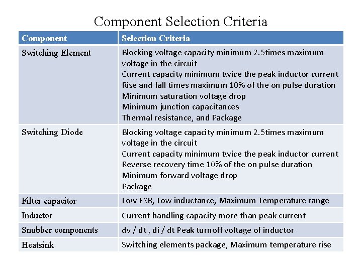
Component Selection Criteria Switching Element Blocking voltage capacity minimum 2. 5 times maximum voltage in the circuit Current capacity minimum twice the peak inductor current Rise and fall times maximum 10% of the on pulse duration Minimum saturation voltage drop Minimum junction capacitances Thermal resistance, and Package Switching Diode Blocking voltage capacity minimum 2. 5 times maximum voltage in the circuit Current capacity minimum twice the peak inductor current Reverse recovery time 10% of the on pulse duration Minimum forward voltage drop Package Filter capacitor Low ESR, Low inductance, Maximum Temperature range Inductor Current handling capacity more than peak current Snubber components dv / dt , di / dt Peak turnoff voltage of inductor Heatsink Switching elements package, Maximum temperature rise

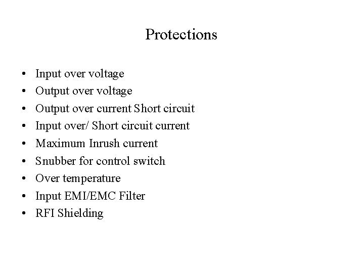
Protections • • • Input over voltage Output over current Short circuit Input over/ Short circuit current Maximum Inrush current Snubber for control switch Over temperature Input EMI/EMC Filter RFI Shielding

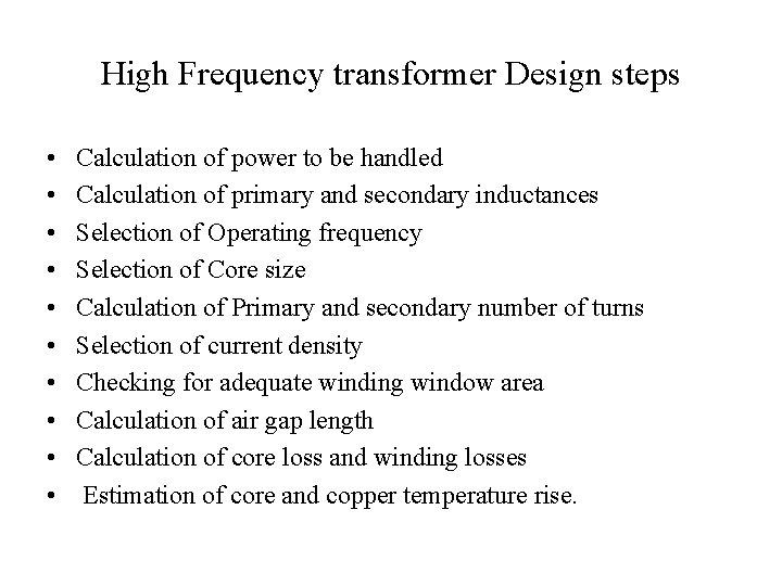
High Frequency transformer Design steps • • • Calculation of power to be handled Calculation of primary and secondary inductances Selection of Operating frequency Selection of Core size Calculation of Primary and secondary number of turns Selection of current density Checking for adequate winding window area Calculation of air gap length Calculation of core loss and winding losses Estimation of core and copper temperature rise.