Design and Implementation of VLSI Systems EN 1600
- Slides: 12

Design and Implementation of VLSI Systems (EN 1600) Lecture 32: Pad Frame Design and Packaging Prof. Sherief Reda Division of Engineering, Brown University Spring 2008 [sources: Weste/Addison Wesley – Tanner Manual] S. Reda EN 1600 SP’ 08

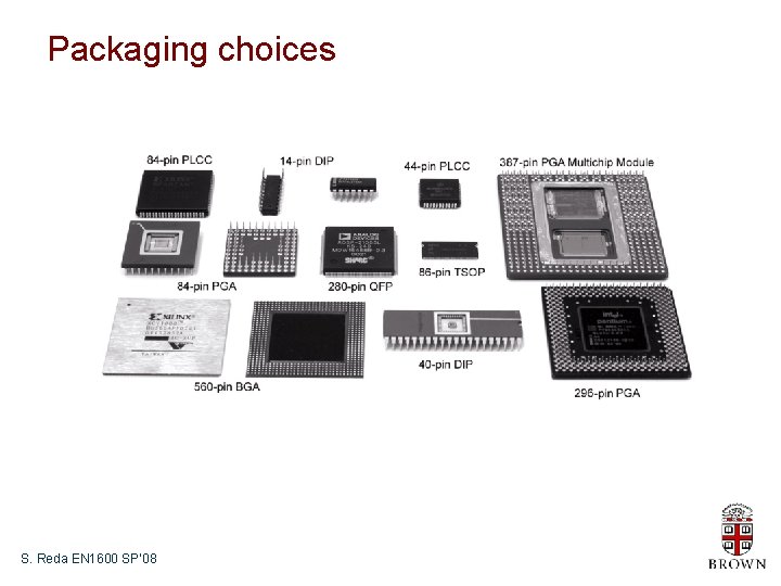
Packaging choices S. Reda EN 1600 SP’ 08

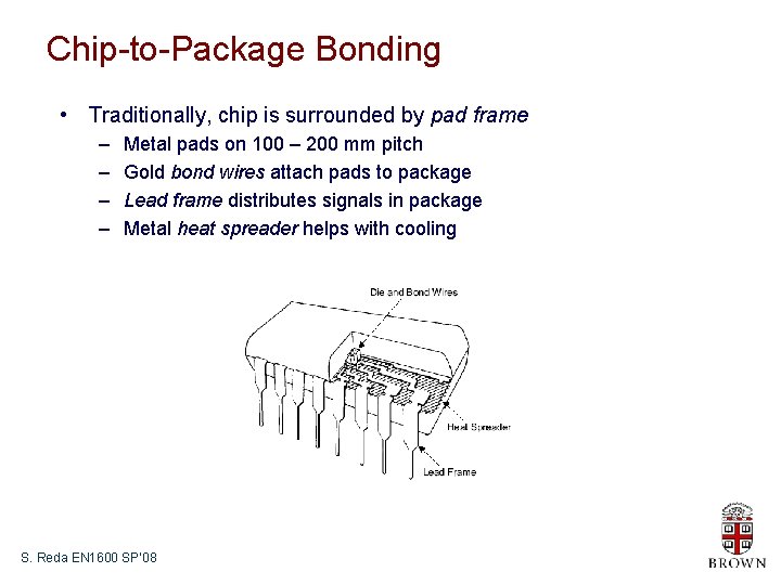
Chip-to-Package Bonding • Traditionally, chip is surrounded by pad frame – – Metal pads on 100 – 200 mm pitch Gold bond wires attach pads to package Lead frame distributes signals in package Metal heat spreader helps with cooling S. Reda EN 1600 SP’ 08

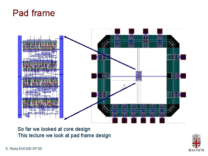
Pad frame So far we looked at core design This lecture we look at pad frame design S. Reda EN 1600 SP’ 08

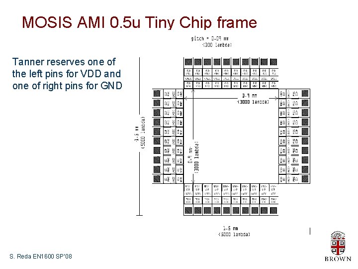
MOSIS AMI 0. 5 u Tiny Chip frame Tanner reserves one of the left pins for VDD and one of right pins for GND S. Reda EN 1600 SP’ 08

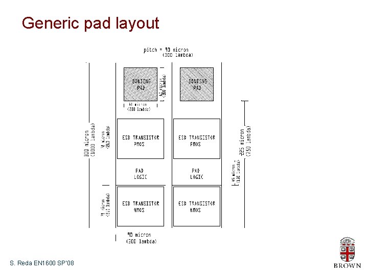
Generic pad layout S. Reda EN 1600 SP’ 08

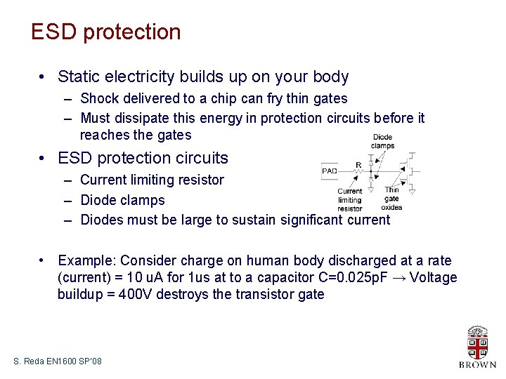
ESD protection • Static electricity builds up on your body – Shock delivered to a chip can fry thin gates – Must dissipate this energy in protection circuits before it reaches the gates • ESD protection circuits – Current limiting resistor – Diode clamps – Diodes must be large to sustain significant current • Example: Consider charge on human body discharged at a rate (current) = 10 u. A for 1 us at to a capacitor C=0. 025 p. F → Voltage buildup = 400 V destroys the transistor gate S. Reda EN 1600 SP’ 08

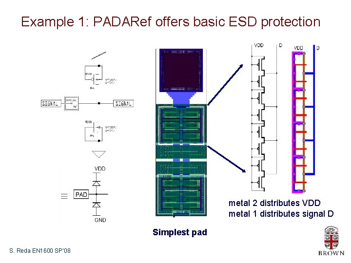
Example 1: PADARef offers basic ESD protection metal 2 distributes VDD metal 1 distributes signal D Simplest pad S. Reda EN 1600 SP’ 08

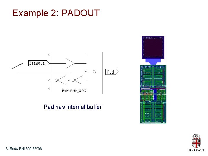
Example 2: PADOUT Pad has internal buffer S. Reda EN 1600 SP’ 08

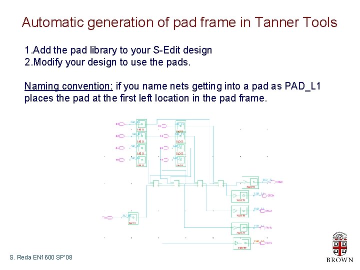
Automatic generation of pad frame in Tanner Tools 1. Add the pad library to your S-Edit design 2. Modify your design to use the pads. Naming convention: if you name nets getting into a pad as PAD_L 1 places the pad at the first left location in the pad frame. S. Reda EN 1600 SP’ 08

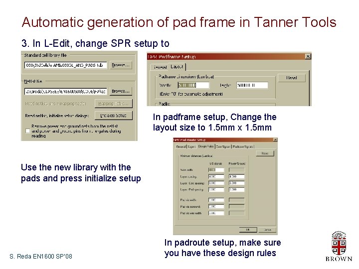
Automatic generation of pad frame in Tanner Tools 3. In L-Edit, change SPR setup to In padframe setup, Change the layout size to 1. 5 mm x 1. 5 mm Use the new library with the pads and press initialize setup S. Reda EN 1600 SP’ 08 In padroute setup, make sure you have these design rules

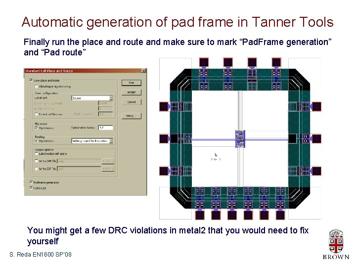
Automatic generation of pad frame in Tanner Tools Finally run the place and route and make sure to mark “Pad. Frame generation” and “Pad route” You might get a few DRC violations in metal 2 that you would need to fix yourself S. Reda EN 1600 SP’ 08