Design and Implementation of VLSI Systems EN 1600
- Slides: 13

Design and Implementation of VLSI Systems (EN 1600) Lecture 08 Prof. Sherief Reda Division of Engineering, Brown University Spring 2008 [sources: Weste/Addison Wesley – Rabaey/Pearson]

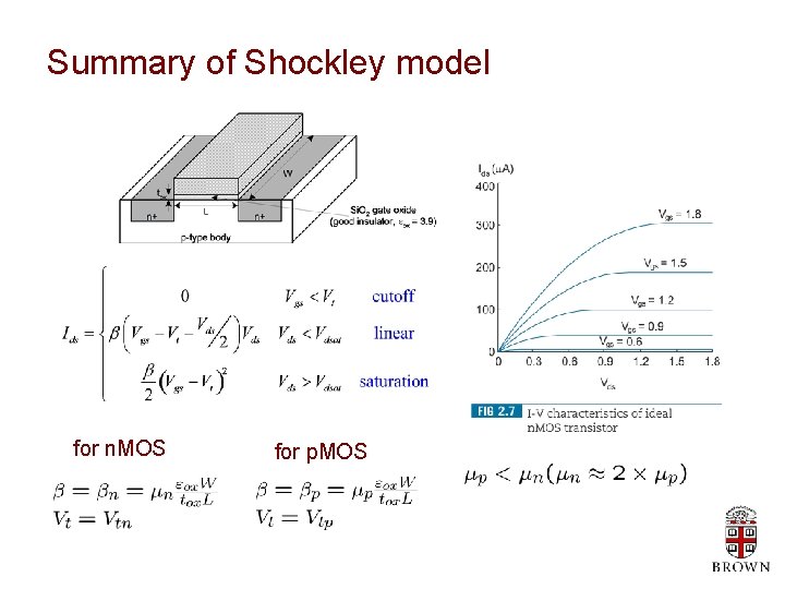
Summary of Shockley model for n. MOS for p. MOS

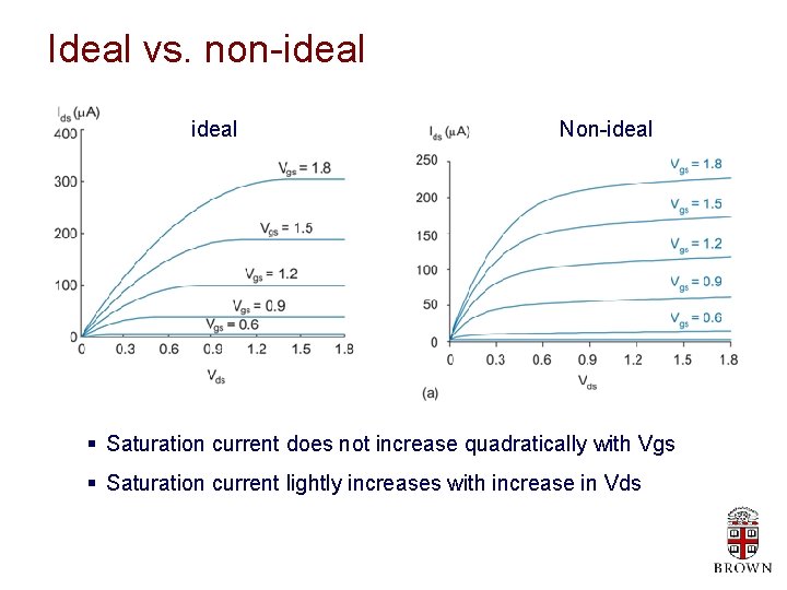
Ideal vs. non-ideal Non-ideal § Saturation current does not increase quadratically with Vgs § Saturation current lightly increases with increase in Vds

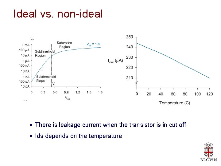
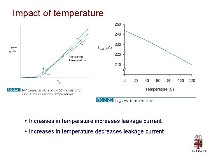
Ideal vs. non-ideal § There is leakage current when the transistor is in cut off § Ids depends on the temperature

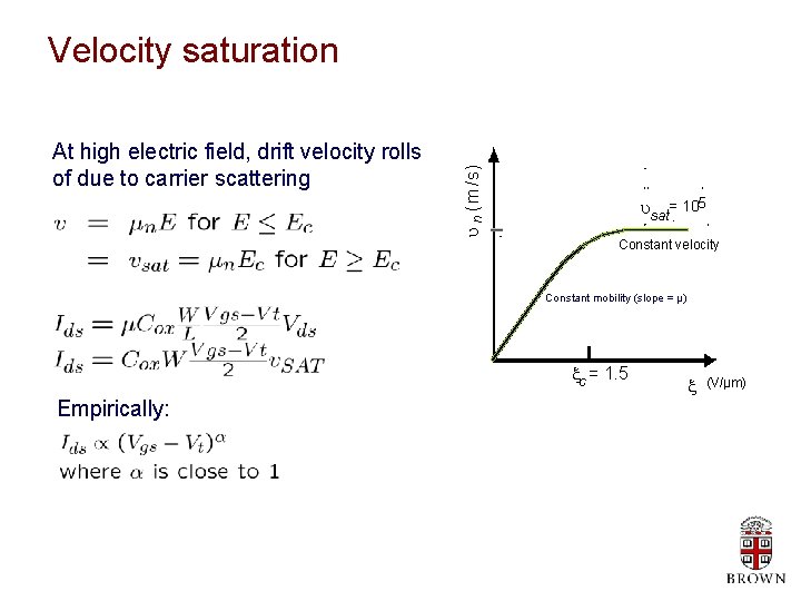
At high electric field, drift velocity rolls of due to carrier scattering u n (m /s) Velocity saturation usat= 105 Constant velocity Constant mobility (slope = µ) xc = 1. 5 Empirically: x (V/µm)

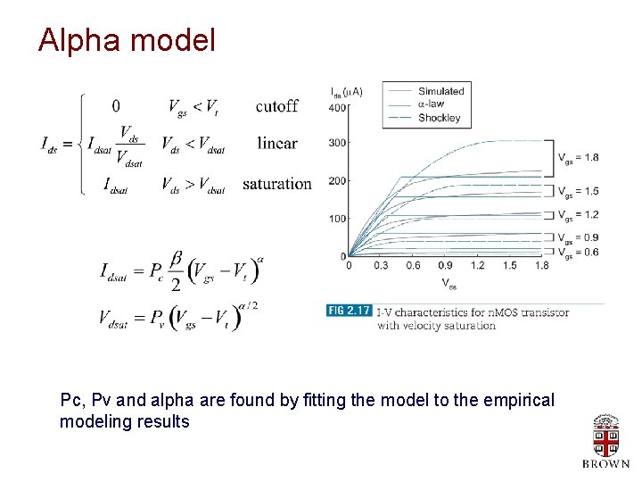
Alpha model Pc, Pv and alpha are found by fitting the model to the empirical modeling results

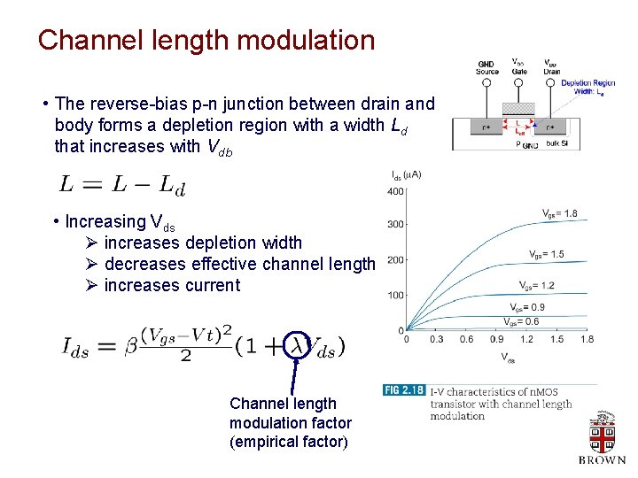
Channel length modulation • The reverse-bias p-n junction between drain and body forms a depletion region with a width Ld that increases with Vdb • Increasing Vds Ø increases depletion width Ø decreases effective channel length Ø increases current Channel length modulation factor (empirical factor)

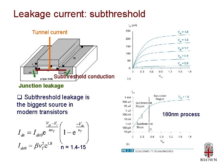
Leakage current: subthreshold Tunnel current polysilicon gate W t ox n+ L p-type body n+ Subthreshold conduction Junction leakage q Subthreshold leakage is the biggest source in modern transistors n = 1. 4 -15 180 nm process

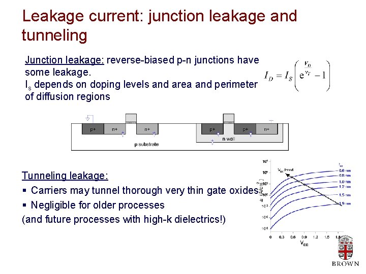
Leakage current: junction leakage and tunneling Junction leakage: reverse-biased p-n junctions have some leakage. Is depends on doping levels and area and perimeter of diffusion regions Tunneling leakage: § Carriers may tunnel thorough very thin gate oxides § Negligible for older processes (and future processes with high-k dielectrics!)

Impact of temperature • Increases in temperature increases leakage current • Increases in temperature decreases leakage current

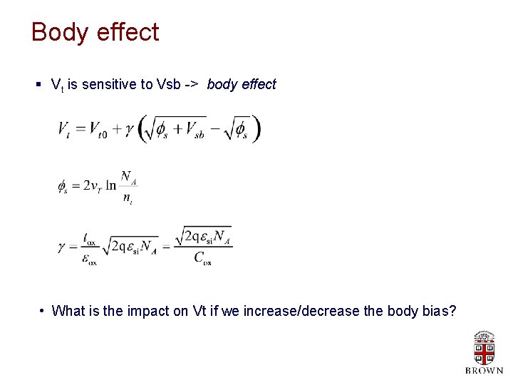
Body effect § Vt is sensitive to Vsb -> body effect • What is the impact on Vt if we increase/decrease the body bias?

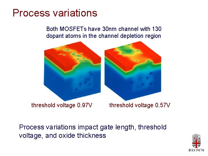
Process variations Both MOSFETs have 30 nm channel with 130 dopant atoms in the channel depletion region threshold voltage 0. 97 V threshold voltage 0. 57 V Process variations impact gate length, threshold voltage, and oxide thickness

Summary § § Ideal transistor characteristics Non-ideal transistor characteristics Inverter DC transfer characteristics Simulation with SPICE and integration with L-Edit