Communications Devices Lecture on 623 627 630 77


, magnetic")
, magnetic")
,")


 is in")


 such as electrical")
 of the expected value is")
- Slides: 35
Communications Devices Lecture on 6/23, 6/27, 6/30, 7/7, 7/14, 7/21 in 2015 Hirohito YAMADA
About lecture 1. Schedule 6/23 Basic of semiconductor photonic devices 6/27 Matter-electromagnetic wave interaction based on semi-classical theory 6/30 Electromagnetic field quantization and quantum theory 7/7 Optical transition in semiconductor, Photo diode, Laser diode 7/14 Optical amplifier, Optical modulator, Optical switch, Optical wavelength filter, and Optical multiplexer/demultiplexer 7/21 Summary 2. Textbook written in Japanese 米津 宏雄 著、光通信素子 学 - 発光・受光素子 -、 学図書 霜田 光一 編著、量子エレクトロニクス、裳華房 山田 実著、電子・情報 学講座 15 光通信 学、培風館 伊藤弘昌 編著、フォトニクス基礎、朝倉書店 第 5章 3. Questions E-mail: yamada@ecei. tohoku. ac. jp, or ECEI 2 nd Bld. Room 203 4. Lecture note dounload URL: http: //www 5 a. biglobe. ne. jp/~babe
Data traffic explosion on the Internet Trend of data traffic processed by a domestic network node Data rate (Gbit/s) Rapid increase of double per 2. 5 years Double/5 years double/year Double/3 years M/D/Y http: //www. jpix. ad. jp/en/technical/traffic. html
Growth of internet traffic in Japan Total download traffic in Japan was about 2. 6 T bps at the end of 2013 Daily average value Annual growth rate: 30% Total download traffic in Japan Total upload traffic in Japan 2004 2005 2006 2007 2008 2009 year 2010 2011 2012 2013 Cited from: H 26年度版情報通信白書
Optical fiber submarine networks Cited from http: //www 1. alcatel-lucent. com/submarine/refs/index. htm
Power consumption forecast of network equipments on i t p Total power generation m su n at 2007 o r c e fic w f o a P tr k r o tw e N Total internet traffic (Tbps) Annual power consumption of network equipments (× 1011 Wh) Domestic internet traffic is increasing 40%/year If increasing trend continue, by 2024, power consumption of ICT equipments will exceed total power generation at 2007 year http: //www. aist-victories. org/jp/about/outline. html
Expanding applied area of optical communication Nowadays, application area of optical communications are spreading from rack-to-rack of server to universal-bass-interface of PCs Backplane of a server (Orange color cables are optical fibers) Universal Bass interface (Light Peak) installed in SONY VAIO Z
Photonic devices used for optical communications Various optical devices for use in optical networks 1. Passive optical device, Passive photonic device - Optical waveguide, optical fiber - Optical splitter : Treated in our lecture - Optical directional coupler - Optical wavelength filter - Wavelength multiplexer/demultiplexer (MUX/DEMUX) - Light polarizer - Wave plate - Dispersion control device - Optical attenuator - Optical isolator - Optical circulator - Optical switch, Photonic switch - Photo detector, Photo diode (PD) 2. Active optical device, Active photonic device - Light-emitting diode (LED) - Semiconductor laser, Laser diode (LD) - Optical amplifier 3. Other devices(Wavelength converter, Optical coherent receiver, etc. )
Photonic devices: supporting life of 21 st century Various photonic devices used for applications other than optical communication - charge-coupled device (CCD) image sensor - CMOS image sensor - solar cell, photovoltaic cell - photo-multiplier - image pick-up tube - CRT: cathode-ray tube, Braun tube - liquid crystal display (LCD) - plasma display - organic light emitting display - various recording materials (CD, DVD, BLD, hologram, film, bar-code) - various lasers (gas laser, solid laser, liquid laser) - non-linear optical devices These devices collectively means “Photonic devices”
What is Photonic Device ? Manipulating electron charge Electronics Magnetic Recording voltage and current Manipulating Electron Tube, Diode, Tr, FET, LSIwavefunction of electron Tunnel effect devices Manipulating both spin and Spintronics charge of GMR HDD electrons MRAM Photo-electronics (Opt-electronics) Display CCD, CMOS sensor Manipulating photon and solar cell electron charge LD, LED Unexplored Photo detector, PD Manipulating photon Magnetics Photonics Opto-spinics Energy and number Laser magnet-optical HDD Optical disk Electromagnetic disk Magnetic tape wave Optical fiber Manipulating spin amplitude and of materials phase ?
Basis of semiconductor photonic devices Properties required for semiconductor used as photonic devices Passive devices(Non light-emitting devices) ・ Small nonlinear optical effect (as distinct from nonlinear optical devices) ・ Better for small material dispersion ・ Small birefringence (polarization independence) Active devices(Light-emitting devices) ・ Moderately-opaque at operating wavelength ・ High radiant transition probability in case of light-emitting devices (Direct transition semiconductor ) ・ To be obtained pn-junction (To be realized current injection devices) Optical absorption coefficient: α (cm-1) ・ Transparent at operating wavelength 105 T = 300 K Si 104 In 0. 53 Ga 0. 47 As Ga. As In. P Ge 103 102 0. 4 0. 6 0. 8 1. 0 1. 2 1. 4 1. 6 Wavelength: λ (μm) Optical absorption coefficient of major semiconductor materials
Band structure of semiconductors Semiconductor and band structure According to Bloch theorem, wave function of an electrons in crystal is described as a quantum number called “wave number” This predicts existing dispersion relation between energy and wave number of electron. This relation is called energy band (structure) Electron Hole In bulk Si, holes distribute at around the Γ point, on the other hand, electrons distribute at around the X point (Indirect transition semiconductors) Band gap ~1. 1 e. V Dispersion relation of electron energy in Si
Band structure of semiconductors Band structure of compound semiconductors Both electrons and holes distribute at around the Γ point (Direct transition semiconductors) Electron Hole Ga. As In. P
Band structure of semiconductors Band structure of Ge Ge which is group Ⅳ semiconductor is also indirect transition type semiconductor, but by adding tensile strain, it changes a direct transition-like band structure Recent year, Ge laser diode(RT, Pulse) was realized by current injection Band structure of Ge Conduction band Indirect transition Direct transition 1. 6% tensile strain Valence band
Basis of semiconductor photonic devices Material dispersion Values of dielectric constant (refractive index), magnetic permeability depend on frequency of electromagnetic wave interacting with the material Dielectric constant (refractive index) significantly changes at the resonance frequency of materials. In linear response, between real part and imaginary part of frequency response function holds Kramers-Kronig relation. Real part Material equation Photon energy (e. V) Phenomenologically-derived equation of relation between wavelength and refractive index Imaginary part W. Sellmeier equation Here, λi = c/νi, c: light speed, νi: resonance frequency of material, Ai: Constant Calc. Photon energy (e. V) Calculation of dielectric function ε of Si
Basis of semiconductor photonic devices Birefringence In anisotropic medium, dielectric constant (refractive index), magnetic permeability are tensor (Material equation) Incident ray Crystal is optically anisotropic medium When light beam enter a crystal, it splits two beams (ordinary ray and extraordinary ray) Optical axis Outgoing ray extraordinary ray ordinary ray In birefringence crystals, an incident direction where light beam does not split is called optical axis (correspond to c-axis of the crystal) Birefringence of calcite
Basis of semiconductor photonic devices Nonlinear optical effect Values of dielectric constant (refractive index), magnetic permeability depend on amplitude of electromagnetic field interacting with the material Material equation When strong electric field (light) applied to a material, nonlinear optical effects emerge. Wavelength conversion devices use this effects. When intensity of incident light is weak, linear polarization P which proportional to the electric field E is induced. Linear polarization c : Electric susceptibility When intensity of incident light become strong, electric susceptibility become depended on the electric field E
Basis of semiconductor photonic devices Electron transition in direct transition type and indirect transition type semiconductors In case of indirect transition, phonon intervenes light emission or absorption Band structure of (a) Ga. As and (b) Si
Light emission from materials Light absorption and emission in material Excited state Nucleus All light come from atoms ! Sun light‥‥Nuclear fusion of hydrogen Fluorescence of fireflies ‥‥Chemical reaction of organic materials Light from burning materials ‥‥ Chemical reaction of organic materials Electroluminescence from LED‥‥Electron transition ΔE in semiconductors Light ν Ground state Excited state Light Ground state ΔE = hν Why materials emit light? You have to learn about interaction mechanism of matter with electromagnetic field if you want to understand these phenomena In the field of Quantum electronics
Light emission from materials According to classical electromagnetics, Rutherford atom model is unstable. It predicts lifetime of atoms are order of 10 -11 sec. (See the final subject in my lecture note ElectromagneticsⅡ) v ω Electron −e m Proton r +e In order to solve this antinomy, Quantum mechanics was proposed N. Bohr proposed an atom model which electrons exist as standing wave of matter-wave. The shape of the standing wave is defined by the quantum condition, and it is arrowed in several discreet states. When an electron transits from one steady state to other state, it emit / absorb photon which energy correspond to energy difference between the two states. (ΔE = hν) Rutherford atom model Proton −e +e Which process occur ? Light emission or absorption ? Why electrons make transition between the states ? Bohr hydrogen atom model
Theory describing light absorption and emission There are three methods describing interaction of matter with electromagnetic fields 1. Classical theory 2. Semi-classical theory Energy of electrons in semiconductor is quantized (Band structure), On the other hand, energy of electromagnetic field is treated by classical electromagnetics 3. Quantum theory Energy of electrons in semiconductor is quantized (Band structure), Electromagnetic field is also quantized (Field quantization) Three methods and their applicable phenomena Electromagnetic Optical field absorption Stimulated Spontaneous emission Method Matter Classical theory Classical Possible Impossible Semi-classical theory Quantum Classical Possible Impossible Quantum Possible Quantum theory Quantum
Description of electromagnetic field In order to understand interaction of matter with electromagnetic field, we need to describe electromagnetic field and to understand its fundamental characteristics Maxwell equations Electric field E and magnetic field B can be also described as follows with electromagnetic potential A(x, t) and ϕ(x, t) Therefore, Maxwell equations can be replaced to equations with A and ϕ as values of electromagnetic field, instead of E and B
Description of electromagnetic field Electromagnetic potentials can be described as follows with arbitrary scalar function χ(x, t). This function χ(x, t) is called a “gauge function”, and selecting these new electromagnetic potential AL and ϕL is called “gauge transformation”. When χ(x, t) was selected as AL and ϕL satisfying the following relation, the gauge is called “Lorenz gauge”. In this case, basic equations that describe electromagnetic phenomena is reduced to two simple equations regarding AL and ϕL as follows. These equations indicate that electromagnetic potential AL and ϕL caused by ie or e propagate as wave with light speed.
Description of electromagnetic field Other than Lorenz gauge, when A was selected as satisfying condition, the gauge is called “Coulomb gauge”. In this case, basic equations that describe electromagnetic phenomena is as follows In free space where both electric charge ρe and electric current ie do not exist, Therefore, E and B is derived from A with the following relations By selecting Coulomb gauge, electromagnetic fields can be described by only vector potential A, because scalar potential ϕ is constant in whole space when electric charge dose not exist in the thinking space.
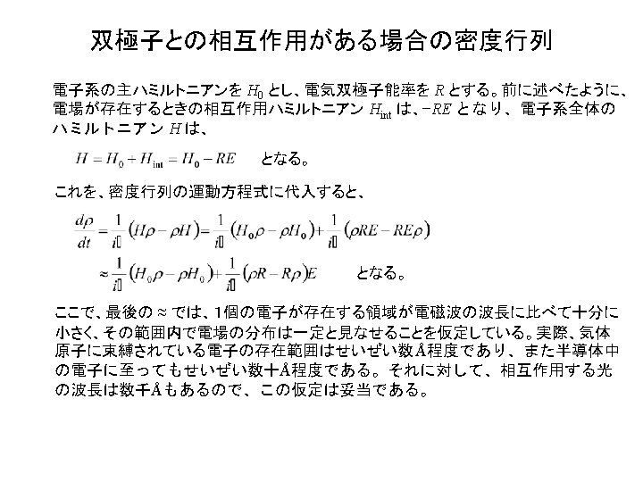
Interaction of charged particles with electromagnetic fields When single charged particle (electron) is in electromagnetic field, Hamiltonian of the particle is described as follows Here, p is the momentum operator, m is electron mass, V is potential of electron, e is elementary charge, and A is vector potential. Hamiltonian H can be also written as, Here, H 0 is an Unperturbed Hamiltonian which is for an electron in space without electromagnetic field, and Hint is an Interaction Hamiltonian which is originated by interaction between an electron and electromagnetic field. The last term in Hint is proportional to A 2, and it reveals higher order effects (nonlinear optical effect). Here, we ignore it because the contribution is small.
Electrical-dipole approximation of the interaction Position of a charged particle is described as Momentum of a charged particle is described as Polarization r of electron cloud E Vector potential is described as Polarization of atom +e e+iωt Electric field is E r Therefore, Here, R = er, and it called electric dipole moment e−iωt −e Electrical dipole Terms “ei 2ωt ” or “e−i 2ωt ” disappear when integrating for time
Electrical-dipole approximation of the interaction Interaction Hamiltonian only include effect by electric field “RE” although the derived interaction equation for a charged particle include effects by both electric field (Coulomb force) and magnetic field (Lorentz force). The reason is that we assume the motion of a charged particle as which is vibration at a limited place. If we assume parallel motion for it, effect by magnetic field will be also included. In this way, when the interaction only depend on electric field, and the interaction can be described as RE, it is called electric dipole approximation. In some case, higher order polarization “multipolar” (such as electric quadrupole or electric octopole) occasionally emerge. 皆さんへのメッセージ 学で扱う物理現象は非常に複雑なものが多い。従って、全ての物理現象を取り入 れた完璧な理論を構築することは不可能である。 良きエンジニアとは、それら複雑な物理現象の中で、何が本質的に重要かを見極め、 近似をうまく使い、無視できる物理現象は思い切って無視し、シンプルな理論を構築 できる人である。ただし、どんな近似を使ったのかは決して忘れてはいけない。
Electrical dipole in semiconductor In semiconductor, an electron and hole pair forms a electrical dipole Conduction band Electron −e + Electron Electrical dipole E Electrical dipole +e Hole Valence band Electrical dipole in semiconductor
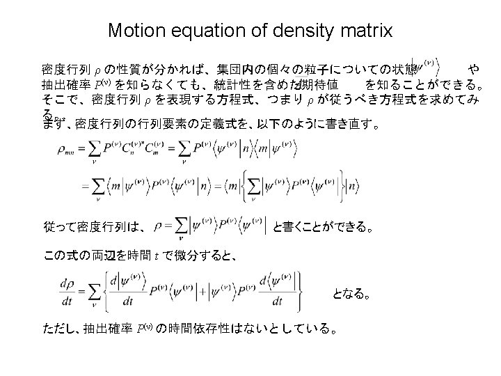
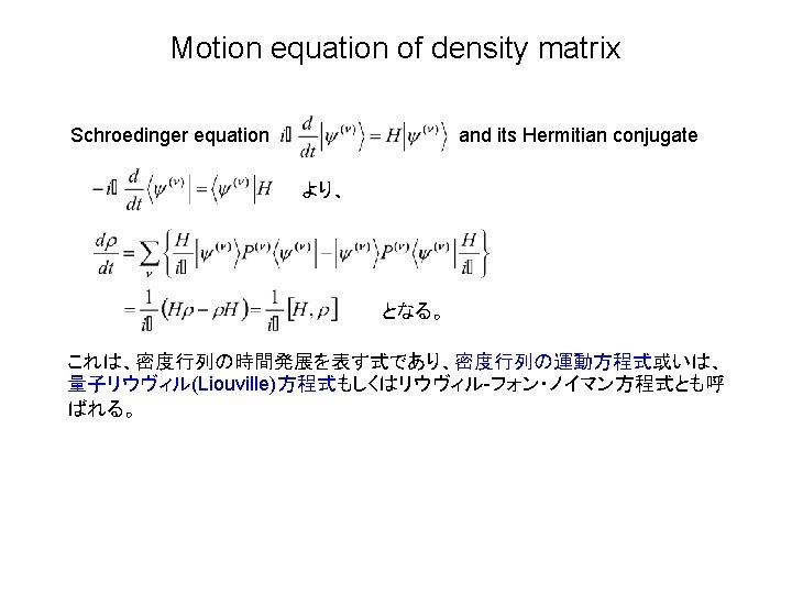
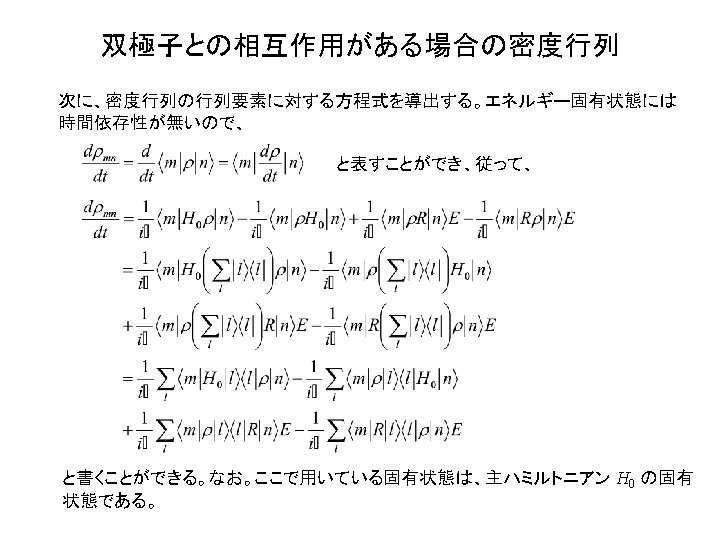
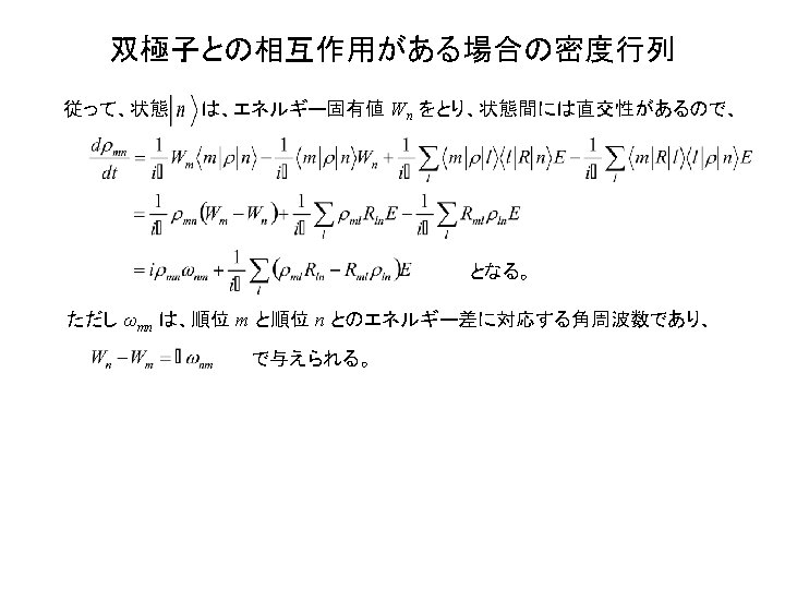
Quantum statistics and density matrix Physical quantities involving many particles (electrons) such as electrical current are statistical average values for the particles. Furthermore, expected values for multiple measurements of a single event is needed statistical treatments. We discuss about statistical nature for many particles or multiple measurements. State for ν th particle or ν th measurement can be described as. Here, is an energy eigenstate for single particle. It is assumed to form complete space. Therefore, any can be formed by linear combination of . does not required the suffix (ν). If operator for a physical quantity is assumed as A, expected value for ν th particle is. Next, we develop an average of expected values for the group of particle (ensemble average). We assume the contribution from the ν the particle (probability for finding n th particle) as P(ν) , and normalize it.
Quantum statistics and density matrix Statistical average (ensemble average) of the expected value is described as Here, we rewrite as below Matrix ρ having ρmn as its elements is called density matrix Using density matrix . is identity operator is summation of on-diagonal elements of ρA, that is Trace. , and