CMOS Detectors with Timing Gianluigi Casse University of
- Slides: 27
CMOS Detectors with Timing Gianluigi Casse University of Liverpool/Fondazione Bruno Kessler, Trento New dimensions in silicon pixel detectors, IOP meeting, Manchester, 19/10/2017. https: //indico. hep. manchester. ac. uk/conference. Time. Table. py? conf. Id=5238#20171019. detailed 1
OUTLINE • Monolithic sensors : suitable for timing? • Design CMOS for timing: • • G. Casse, New dimensions in silicon pixel detectors, IOP meeting, Manchester, 19/10/2017 2
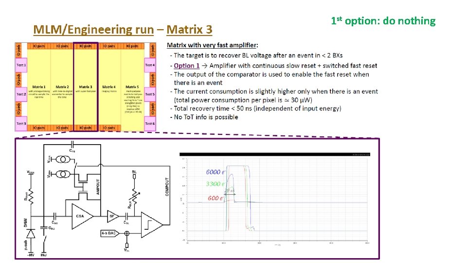
OUTLINE • Monolithic sensors : suitable for timing? • Design CMOS for timing: • 1 st option: do nothing • • • G. Casse, New dimensions in silicon pixel detectors, IOP meeting, Manchester, 19/10/2017 3
OUTLINE • Monolithic sensors : suitable for timing? • Design CMOS for timing: • 1 st option: do nothing • 2 nd option: correction circuit (time walk compensation) • • G. Casse, New dimensions in silicon pixel detectors, IOP meeting, Manchester, 19/10/2017 4
OUTLINE • Monolithic sensors : suitable for timing? • Design CMOS for timing: • 1 st option: do nothing • 2 nd option: correction circuit (time walk compensation) • 3 rd option: analogue sampling • G. Casse, New dimensions in silicon pixel detectors, IOP meeting, Manchester, 19/10/2017 5
OUTLINE • Monolithic sensors : suitable for timing? • Design CMOS for timing: • 1 st option: do nothing • 2 nd option: correction circuit (time walk compensation) • 3 rd option: analogue sampling • 4 rt option: waveform sampling G. Casse, New dimensions in silicon pixel detectors, IOP meeting, Manchester, 19/10/2017 6
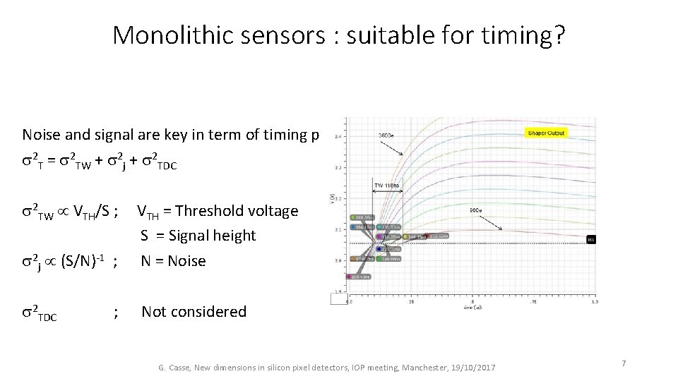
Monolithic sensors : suitable for timing? Noise and signal are key in term of timing performance. s 2 T = s 2 TW + s 2 j + s 2 TDC s 2 TW VTH/S ; s 2 j (S/N)-1 ; VTH = Threshold voltage S = Signal height N = Noise s 2 TDC Not considered ; G. Casse, New dimensions in silicon pixel detectors, IOP meeting, Manchester, 19/10/2017 7
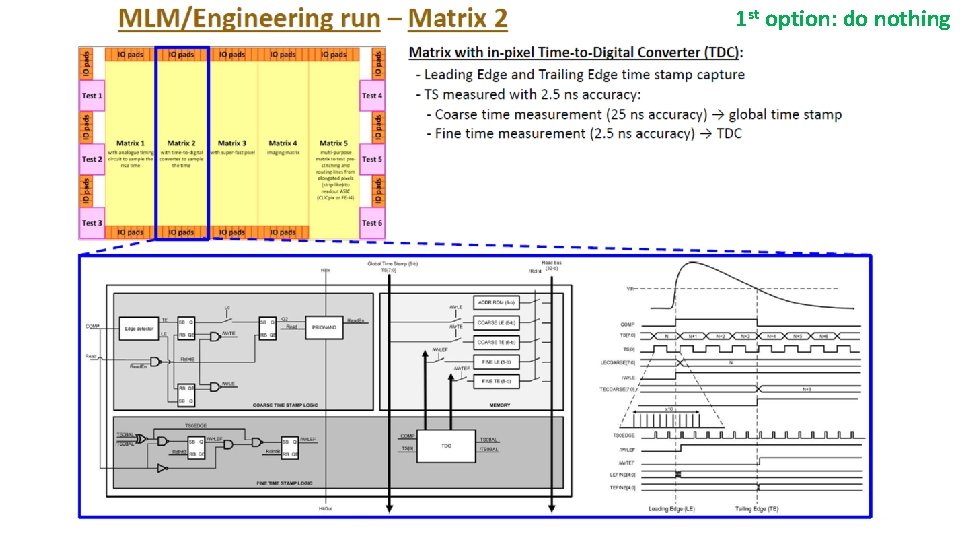
1 st option: do nothing ………………… or better, work on the S/N performance of monolithic devices. Deep depleted MAPS are promising for good S/N, depending on the optimization allowed by the requirements of the application (speed, etc). G. Casse, New dimensions in silicon pixel detectors, IOP meeting, Manchester, 19/10/2017 8
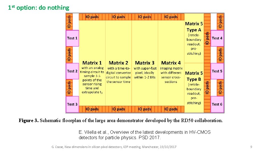
1 st option: do nothing Figure 3. Schematic floorplan of the large area demonstrator developed by the RD 50 collaboration. E. Vilella et al. , Overview of the latest developments in HV-CMOS detectors for particle physics. PSD 2017. G. Casse, New dimensions in silicon pixel detectors, IOP meeting, Manchester, 19/10/2017 9
1 st option: do nothing
1 st option: do nothing
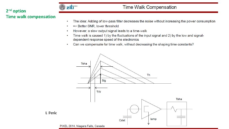
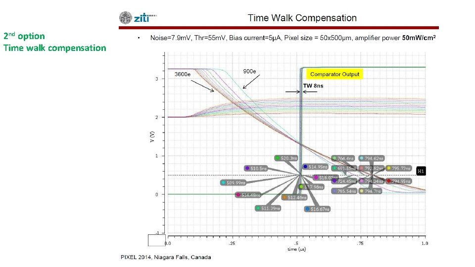
2 nd option Time walk compensation I. Peric
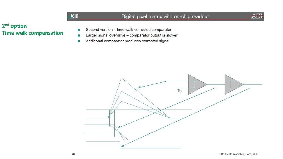
2 nd option Time walk compensation I. Peric
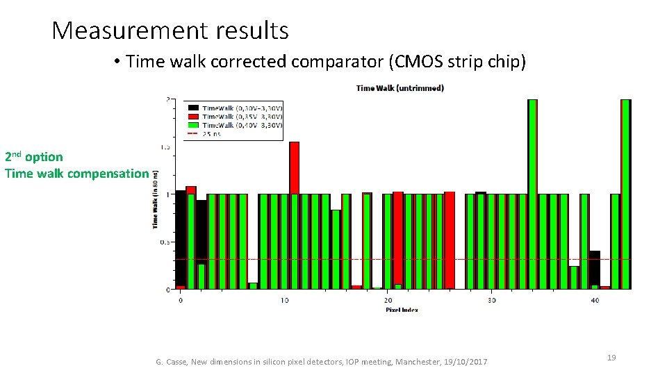
2 nd option Time walk compensation
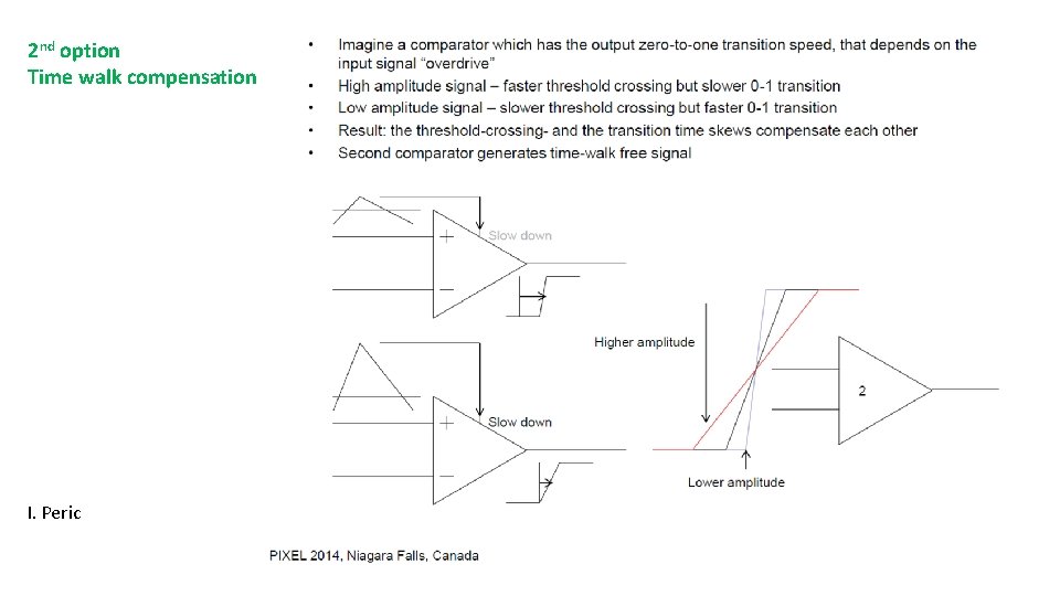
2 nd option Time walk compensation
2 nd option Time walk compensation
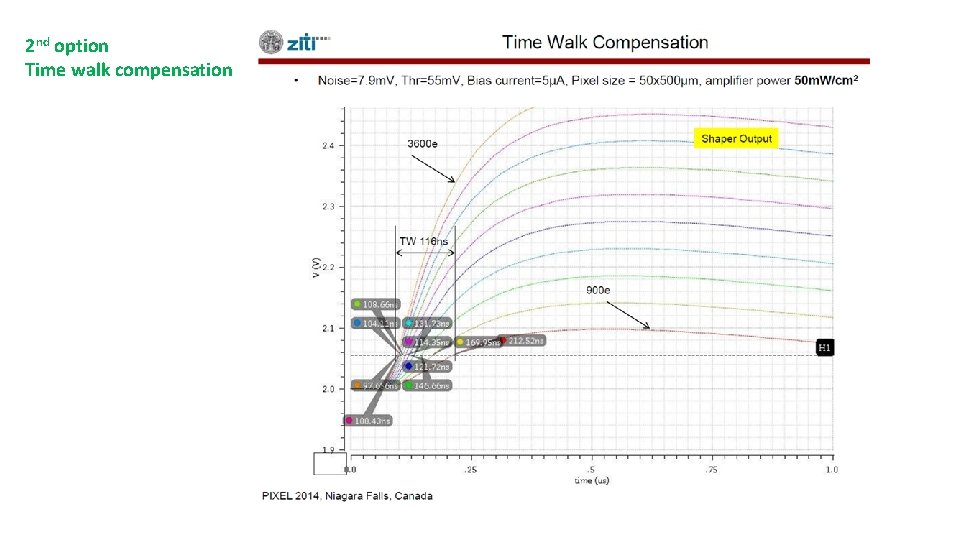
2 nd option Time walk compensation
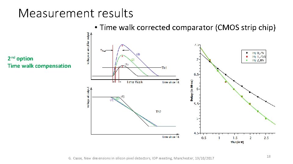
Measurement results • Time walk corrected comparator (CMOS strip chip) 2 nd option Time walk compensation G. Casse, New dimensions in silicon pixel detectors, IOP meeting, Manchester, 19/10/2017 18
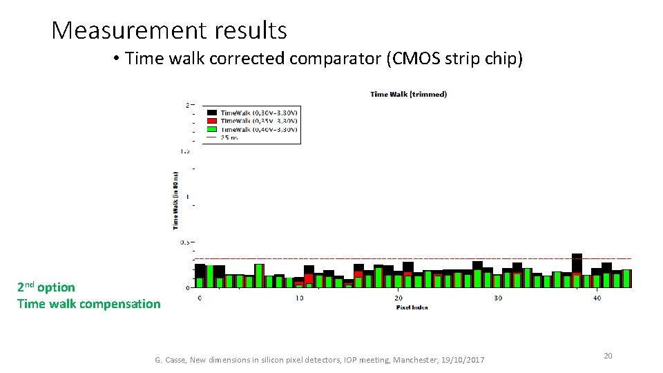
Measurement results • Time walk corrected comparator (CMOS strip chip) 2 nd option Time walk compensation G. Casse, New dimensions in silicon pixel detectors, IOP meeting, Manchester, 19/10/2017 19
Measurement results • Time walk corrected comparator (CMOS strip chip) 2 nd option Time walk compensation G. Casse, New dimensions in silicon pixel detectors, IOP meeting, Manchester, 19/10/2017 20
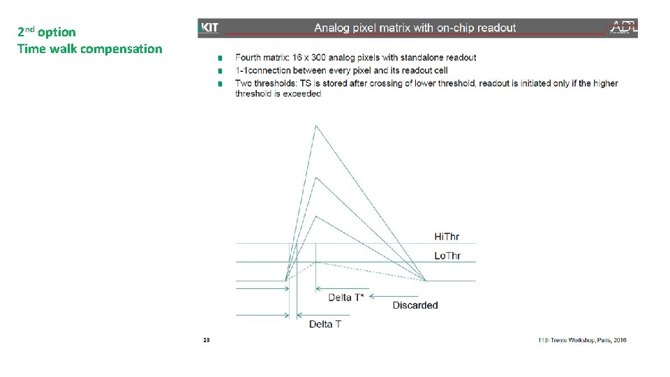
2 nd option Time walk compensation High extra power, relatively large circuit area, increase of parasitic capacitance, introduction of output delay, slow shaping. G. Casse, New dimensions in silicon pixel detectors, IOP meeting, Manchester, 19/10/2017 21
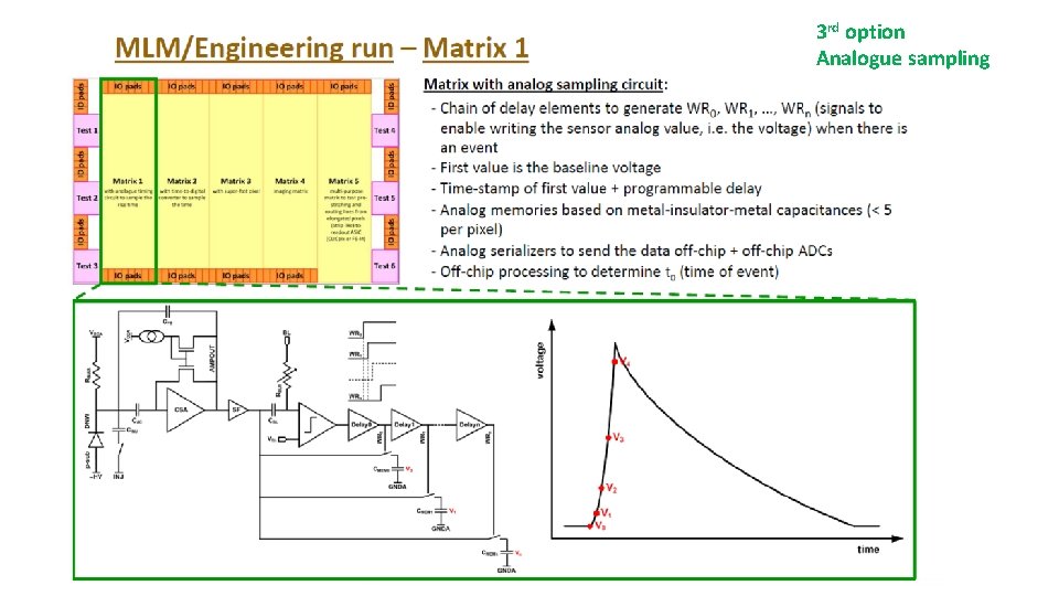
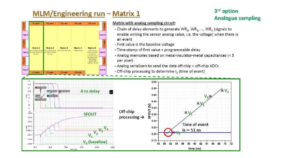
3 rd option Analogue sampling
3 rd option Analogue sampling
3 rd option Analogue sampling Better stability, not applicable to too fast rise times (option fall time? ), compact(ish) design, acceptable power consumption, large output word (bandwidth). G. Casse, New dimensions in silicon pixel detectors, IOP meeting, Manchester, 19/10/2017 24
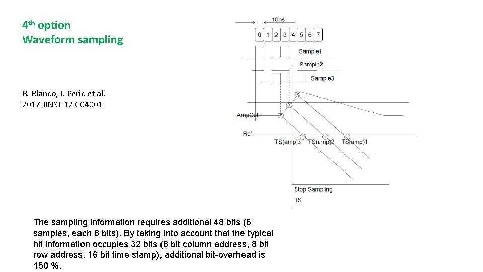
4 th option Waveform sampling R. Blanco, I. Peric et al. 2017 JINST 12 C 04001 The sampling information requires additional 48 bits (6 samples, each 8 bits). By taking into account that the typical hit information occupies 32 bits (8 bit column address, 8 bit row address, 16 bit time stamp), additional bit-overhead is 150 %.
4 th option Waveform sampling Low extra power, slow rate, significant increase in bandwidth, acceptable extra space for the circuit. G. Casse, New dimensions in silicon pixel detectors, IOP meeting, Manchester, 19/10/2017 26
CONCLUSION Good timing with high spatial resolution is one of the challenges that HVCMOS technology can tackle. As the key is signal to noise, the characteristics of deep depleted, monolithic silicon sensor are well suited. Several options are possible: the ‘simplest’ is to improve on the performance, enhancing S/N and pre-amplifier speed. Dedicated in pixel and in sensor circuitry is possible, and it improves time resolution, with some drawbacks that include, at different levels for each solution: larger in-pixel circuits, slower rates, larger bandwidth, higher power consumption (with respect to the do-nothing option). Overall, resolutions in the order of 1 ns seem to be well in sight, the tens of picoseconds require more work, some of which is being carried out. Radiation tolerance? A lot of options, tests ….