VMM Specifications Review Gianluigi De Geronimo Wenxiang Ding

- Slides: 37

VMM Specifications Review Gianluigi De Geronimo, Wenxiang Ding*, Aseem Gupta* George Iakovidis, Venetios Polychronakos Brookhaven National Laboratory, New York, USA * and Stony Brook University, New York, USA October 20 th, 2015

Outline • Block Diagram and Functionality • Pinout and Floorplan • Revision Status and Schedule • Answers to Reviewers' Questions

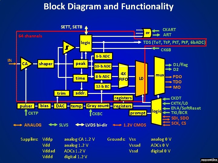
Block Diagram and Functionality SETT, SETB CKART or 64 channels TDS (To. T, Tt. P, Pt. T, Pt. P, 6 b. ADC) logic CK 6 B IN 6 -b ADC CA peak shaper D 1/flag D 2 PDO TDO MO 10 -b ADC 8 -b ADC time 4 X FIFO L 0 mux 12 -b BC trim pulser bias DAC CKTP ANALOG Supplies: Vddp Vddad Vddd addr. temp registers Gray count CKBC SLVS LVDS bi-dir analog CA 1. 2 V analog 1. 2 V ADCs 1. 2 V digital 1. 2 V registers prompt 1. 2 V CMOS Grounds: Vssad Vssd logic CKDT CKTK/L 0 ENA/Soft. Reset TKI/BCR SDI, SDO SCK, CS analog 0 V ADCs 0 V digital 0 V

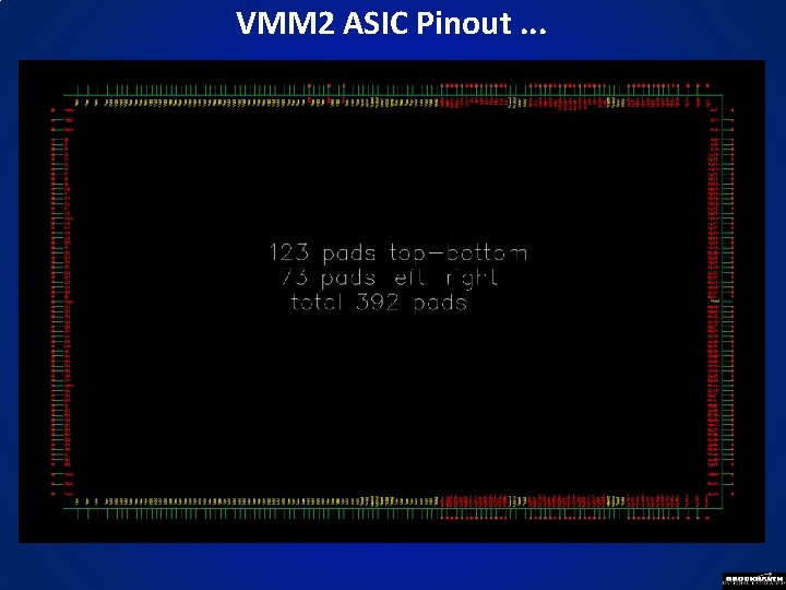
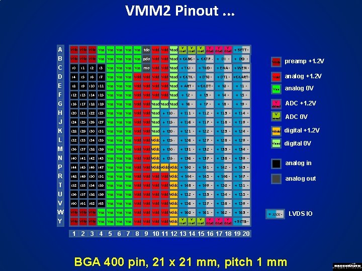
VMM 2 ASIC Pinout. . .

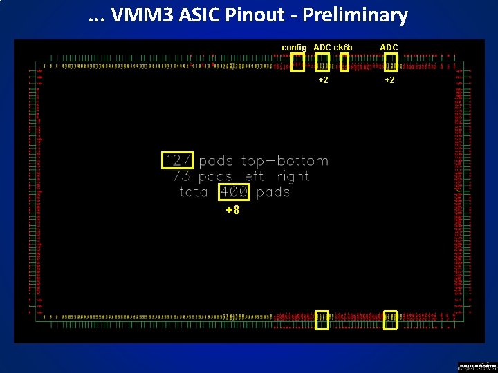
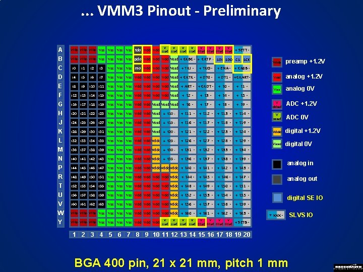
. . . VMM 3 ASIC Pinout - Preliminary config ADC ck 6 b +2 +8 ADC +2

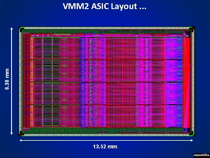
8. 38 mm VMM 2 ASIC Layout. . . 13. 52 mm

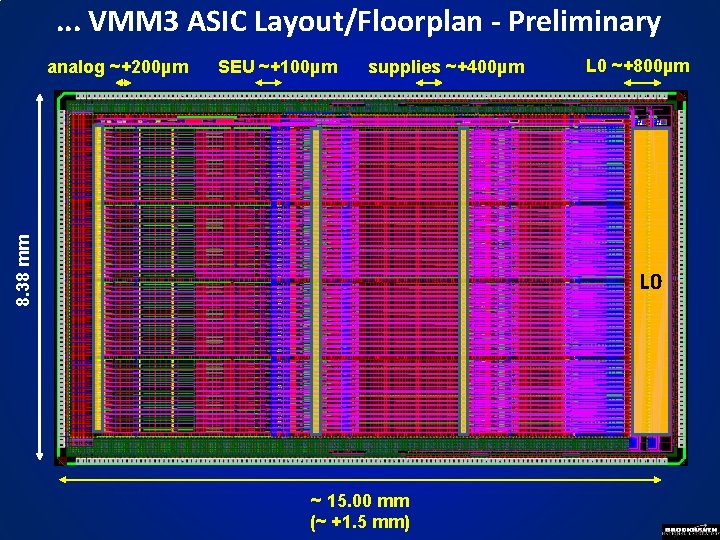
. . . VMM 3 ASIC Layout/Floorplan - Preliminary SEU ~+100µm supplies ~+400µm 8. 38 mm analog ~+200µm L 0 ~+800µm L 0 ~ 15. 00 mm (~ +1. 5 mm)

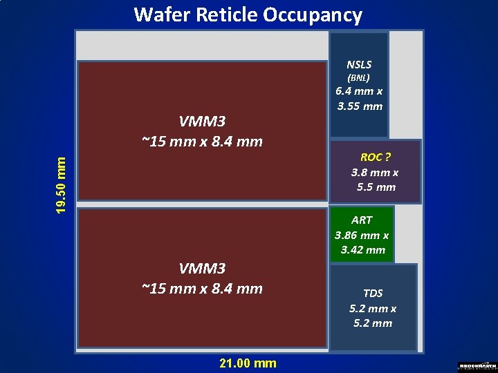
Wafer Reticle Occupancy NSLS (BNL) 19. 50 mm VMM 3 ~15 mm x 8. 4 mm 6. 4 mm x 3. 55 mm ROC ? 3. 8 mm x 5. 5 mm ART 3. 86 mm x 3. 42 mm VMM 3 ~15 mm x 8. 4 mm 21. 00 mm TDS 5. 2 mm x 5. 2 mm

VMM 2 Pinout. . . A B C D E F G H J K L M N P R T U V W Y V V V Vddp Vss Vss Vss tdo Vdd Vssd ssad ddad Vddp Vss Vss Vss pdo Vdd Vssd + CKBC - + CKTP - + DI - + SETT + DO - i 0 i 1 i 2 i 3 Vss Vss mo Vdd Vssd + TKI - + TKO - + ENA - + WEN - i 4 i 5 i 6 i 7 Vss Vss Vdd Vdd Vssd + CKTK - + DT 0 - + DT 1 - +CKART- i 8 i 9 i 10 i 11 Vss Vss Vdd Vdd Vssd + ART - + CKDT - + t 0 - + t 1 - i 12 i 13 i 14 i 15 Vss Vss Vdd Vdd Vssd + t 2 - + t 3 - + t 4 - + t 5 - i 16 i 17 i 18 i 19 Vss Vss Vdd Vssd + t 6 - + t 7 - + t 8 - + t 9 - i 20 i 21 i 22 i 23 Vss Vss Vdd Vssd + t 10 - + t 11 - + t 12 - + t 13 - + t 14 - i 24 i 25 i 26 i 27 Vss Vss Vdd Vssd + t 15 - + t 16 - + t 17 - + t 18 - + t 19 - i 28 i 29 i 30 i 31 Vss Vss Vdd Vssd + t 20 - + t 21 - + t 22 - + t 23 - + t 24 - i 32 i 33 i 34 i 35 Vss Vss Vdd Vddd + t 25 - + t 26 - + t 27 - + t 28 - + t 29 - i 36 i 37 i 38 i 39 Vss Vss Vdd Vddd + t 30 - + t 31 - + t 32 - + t 33 - + t 34 - i 40 i 41 i 42 i 43 Vss Vss Vdd Vddd + t 35 - + t 36 - + t 37 - + t 38 - + t 39 - i 44 i 45 i 46 i 47 Vss Vss Vdd Vddd + t 40 - + t 41 - + t 42 - + t 43 - i 48 i 49 i 50 i 51 Vss Vss Vdd Vdd Vddd + t 44 - + t 45 - i 52 i 53 i 54 i 55 Vss Vss Vdd Vdd Vddd + t 48 - + t 49 - + t 50 - + t 51 - i 56 i 57 i 58 i 59 Vss Vss Vdd Vdd Vddd + t 52 - + t 53 - + t 54 - + t 55 - i 60 i 61 i 62 i 63 Vss Vss Vdd Vdd Vddd + t 56 - + t 57 - + t 58 - + t 59 - + t 46 - Vddp Vdd analog +1. 2 V Vss analog 0 V V ddad ADC +1. 2 V V ssad ADC 0 V Vddd digital +1. 2 V Vssd digital 0 V analog in + t 47 - Vddp Vss Vss Vdd Vdd Vddd + t 60 - + t 61 - + t 62 - + t 63 - Vddp Vss Vss Vdd Vdd Vddd V V V ssad ddad preamp +1. 2 V analog out + xxx - + SETB - 1 2 3 4 5 6 7 8 9 10 11 12 13 14 15 16 17 18 19 20 BGA 400 pin, 21 x 21 mm, pitch 1 mm LVDS IO

. . . VMM 3 Pinout - Preliminary A B C D E F G H J K L M N P R T U V W Y V V V V Vddp Vss Vss tdo Vdd ssad ddad Vddp Vss Vss pdo Vdd Vdd Vssd + SETT - + CKBC - + CKTP - SDI SDO CS SCK i 0 i 1 i 2 i 3 Vss Vss mo Vdd Vdd Vssd + TKI - + TKO - + ENA - + CK 6 B - i 4 i 5 i 6 i 7 Vss Vss Vdd Vdd Vssd + CKTK - + DT 0 - + DT 1 - +CKART- i 8 i 9 i 10 i 11 Vss Vss Vdd Vdd Vssd + ART - + CKDT - + t 0 - + t 1 - i 12 i 13 i 14 i 15 Vss Vss Vdd Vdd Vssd + t 2 - + t 3 - + t 4 - + t 5 - i 16 i 17 i 18 i 19 Vss Vss Vdd Vssd + t 6 - + t 7 - + t 8 - + t 9 - i 20 i 21 i 22 i 23 Vss Vss Vdd Vssd + t 10 - + t 11 - + t 12 - + t 13 - + t 14 - i 24 i 25 i 26 i 27 Vss Vss Vdd Vssd + t 15 - + t 16 - + t 17 - + t 18 - + t 19 - i 28 i 29 i 30 i 31 Vss Vss Vdd Vssd + t 20 - + t 21 - + t 22 - + t 23 - + t 24 - i 32 i 33 i 34 i 35 Vss Vss Vdd Vddd + t 25 - + t 26 - + t 27 - + t 28 - + t 29 - i 36 i 37 i 38 i 39 Vss Vss Vdd Vddd + t 30 - + t 31 - + t 32 - + t 33 - + t 34 - i 40 i 41 i 42 i 43 Vss Vss Vdd Vddd + t 35 - + t 36 - + t 37 - + t 38 - + t 39 - i 44 i 45 i 46 i 47 Vss Vss Vdd Vddd + t 40 - + t 41 - + t 42 - + t 43 - i 48 i 49 i 50 i 51 Vss Vss Vdd Vdd Vddd + t 44 - + t 45 - i 52 i 53 i 54 i 55 Vss Vss Vdd Vdd Vddd + t 48 - + t 49 - + t 50 - + t 51 - i 56 i 57 i 58 i 59 Vss Vss Vdd Vdd Vddd + t 52 - + t 53 - + t 54 - + t 55 - i 60 i 61 i 62 i 63 Vss Vss Vdd Vdd Vddd + t 56 - + t 57 - + t 58 - + t 59 - Vddp Vss Vss Vdd Vdd Vddd + t 46 - preamp +1. 2 V Vdd analog +1. 2 V Vss analog 0 V V ddad ADC +1. 2 V V ssad ADC 0 V Vddd digital +1. 2 V Vssd digital 0 V analog in + t 47 - + t 60 - + t 61 - + t 62 - + t 63 - V V V V Vddp Vss Vss Vdd Vdd ssad ddad Vddp analog out digital SE IO + xxx - + SETB - 1 2 3 4 5 6 7 8 9 10 11 12 13 14 15 16 17 18 19 20 BGA 400 pin, 21 x 21 mm, pitch 1 mm SLVS IO

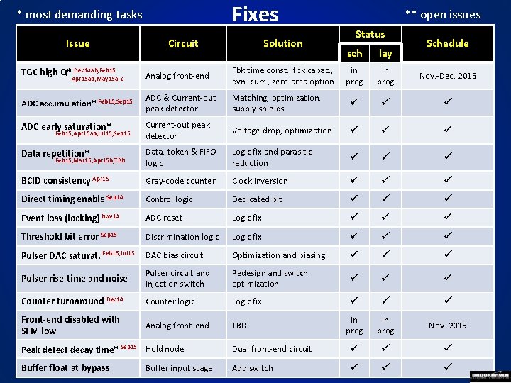
Fixes * most demanding tasks Issue Circuit Solution ** open issues Status Schedule sch lay in prog Nov. -Dec. 2015 TGC high Q* Dec 14 ab, Feb 15 Analog front-end Fbk time const. , fbk capac. , dyn. curr. , zero-area option ADC accumulation * Feb 15, Sep 15 ADC & Current-out peak detector Matching, optimization, supply shields ü ü ü ADC early saturation* Current-out peak detector Voltage drop, optimization ü ü ü Data repetition* Data, token & FIFO logic Logic fix and parasitic reduction ü ü ü BCID consistency Apr 15 Gray-code counter Clock inversion ü ü ü Direct timing enable Sep 14 Control logic Dedicated bit ü ü ü Event loss (locking) Nov 14 ADC reset Logic fix ü ü ü Threshold bit error Sep 15 Discrimination logic Logic fix ü ü ü Pulser DAC saturat. Feb 15, Jul 15 DAC bias circuit Optimization and biasing ü ü ü Pulser rise-time and noise Pulser circuit and injection switch Redesign and switch optimization ü ü ü Counter turnaround Dec 14 Counter logic Logic fix ü ü ü Front-end disabled with SFM low Analog front-end TBD in prog Nov. 2015 Apr 15 ab, May 15 a-c Feb 15, Apr 15 ab, Jul 15, Sep 15 Feb 15, Mar 15, Apr 15 b, TBD Peak detect decay time* Sep 15 Hold node Dual front-end circuit ü ü ü Buffer float at bypass Add switch ü ü ü Buffer input stage

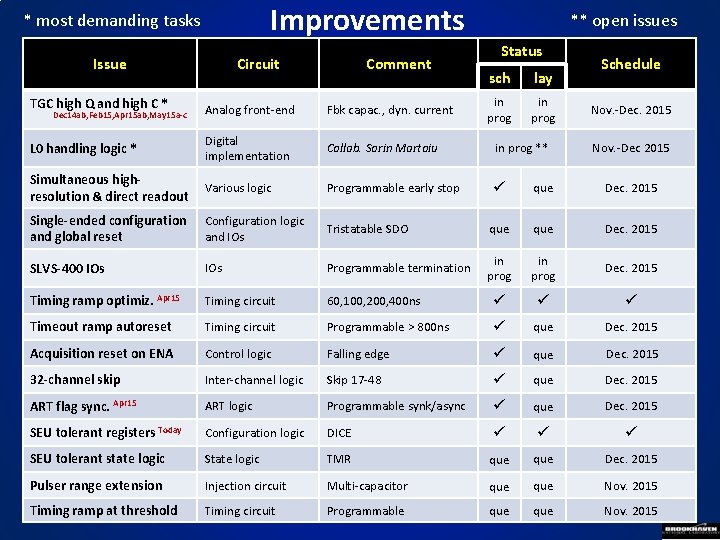
Improvements * most demanding tasks Issue TGC high Q and high C * Circuit Comment ** open issues Status sch lay in prog Schedule Analog front-end Fbk capac. , dyn. current L 0 handling logic * Digital implementation Collab. Sorin Martoiu in prog ** Simultaneous highresolution & direct readout Various logic Programmable early stop ü que Dec. 2015 Single-ended configuration and global reset Configuration logic and IOs Tristatable SDO que Dec. 2015 SLVS-400 IOs Programmable termination in prog Dec. 2015 Timing ramp optimiz. Apr 15 Timing circuit 60, 100, 200, 400 ns ü ü ü Timeout ramp autoreset Timing circuit Programmable > 800 ns ü que Dec. 2015 Acquisition reset on ENA Control logic Falling edge ü que Dec. 2015 32 -channel skip Inter-channel logic Skip 17 -48 ü que Dec. 2015 ART flag sync. Apr 15 ART logic Programmable synk/async ü que Dec. 2015 SEU tolerant registers Today Configuration logic DICE ü ü ü SEU tolerant state logic State logic TMR que Dec. 2015 Pulser range extension Injection circuit Multi-capacitor que Nov. 2015 Timing ramp at threshold Timing circuit Programmable que Nov. 2015 Dec 14 ab, Feb 15, Apr 15 ab, May 15 a-c Nov. -Dec. 2015 Nov. -Dec 2015

References • Sep 14 - https: //indico. cern. ch/event/341396/ • Nov 14 - https: //indico. cern. ch/event/352662/ • Dec 14 a - https: //indico. cern. ch/event/356971/ • Dec 14 b - https: //indico. cern. ch/event/357644/ • Feb 15 - https: //indico. cern. ch/event/371991/ • Mar 15 a - https: //indico. cern. ch/event/379400/ • Mar 15 b - https: //indico. cern. ch/event/382360/ • Mar 15 c - https: //indico. cern. ch/event/383326/ • Apr 15 a - https: //indico. cern. ch/event/384407/ • Apr 15 b - https: //indico. cern. ch/event/388292/ • May 15 - https: //indico. cern. ch/event/395495/ • Jul 15 - https: //indico. cern. ch/event/436227/ • Sep 15 - https: //indico. cern. ch/event/447077/ • Today - this presentation • TBD - W. Ding, next week (tentative)

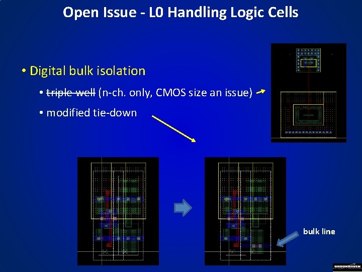
Open Issue - L 0 Handling Logic Cells • Digital bulk isolation • triple well (n-ch. only, CMOS size an issue) • modified tie-down bulk line

Answers to Reviewers' Questions

Answers to Stefan Haas' Concerns 1/2 1) There seem to be two pin list in the specification (table 1 and 3). This is confusing, I assume table 1 is for the previous VMM revision? If so it should be removed. Now the two tables are consistent. Table 1 was the VMM 2 and updated as the design was progressing. 2) The description of the chip configuration should be more detailed. The is no description of the function of the various register bits. Table 6 in the last version addresses this question. 3) In addition the text mentions that ena has to be high in configuration mode, but the diagram shows the signal low. This was caught and fixed. ENA is indeed low for configuration. 4) Also the ENA input is apparently also somehow used to reset the chip, how does this interact with the configuration mode? Soft reset occurs at the ENA transition High to Low. 5) It's not clear if the grouping into strings of 96 bits is relevant, are there any timing constraints for the configuration signals? The SPI sends up to 128 bits in a block. 96 was chosen because the individual channel configuration bits are 24, so an integer number of channels (4) can be configured per block of 96

Answers to Stefan Haas' Concerns 2/2 6) The configuration data output is marked as not used in the NSW, however in the requirements later on this outpur is meant to be used to read for example buffer overflow status bits. Unfortunate choice of words. It is not used because the configuration is not daisy-chained, each chip is configured individually, the do of a selected chip is active but all others are tristated. 7) The text describing the digital readout part seems tobe largely a cut and paste from the requirements document presented at the last review and a lot of important details are missing, for example no configuration registers are described. Yes, it is cut and paste and stated so, until both documents are updated and are consistent with each other. The interface config. registers are now included in V. 2 8) The last part of section 11. 2. 1 remains rather vague, for instance what is the message data format mentioned here? Section 11. 2. 2 mentions a logic simulation of the readout, how far advanced is this? It's not specified in which order the bits from the event builder will be mapped onto the two serial output links. This indeed need to be settled once the adaptation of one level trigger is accepted by ATLAS

Answers to Rick Van Berg's Concerns The interconnections between the chips (and the outside world) are complex and, as we can see from the discussion over the past few weeks, can be confusing. I had initially, been assuming that all of this confusion at the document level was going to be rigorously tested and verified with a behavioral (at least) HDL model of the system, but I have seen no information on such a thing. Does such a model exist or is it planned for the near future? It does not sound easy to handle this level of complex interconnectedness using just documents. Kevin and several of us discussed the need for an overall behavioral model last week when all of us were attending the muon week. It will be done, hopefully, before the final review. One thing that needs to be said is that in reality the interconnections are not as complex as they seem at first glance. And this is because the VMM has four completely independent output data paths. For example the communication between ART and VMM does not affect or is affected by any of the other two chips that the VMM communicates with.

Answers to Francis Anghinolfi's Concerns 1) There is mention of the use of DICE cells. Also the TRM option is considered for some registers or functions. What is the reason to consider DICE cells (compactness, lower cross section, as compared to the TRM ? ). See next slides 20 -24 2) DICE cells are not provided by default in the standard cell of IBM : which kind of DICE cell is used (has it be proven? ) and are these DICE cells compatible with the Place and Route design flow (time model, description files for Encounter) See next slides 20 -24 3) VMM : In document 2015_06_4_VMM 2_Muon. Week_Iakovidis. pdf, on slides 7 and 8 it seems there is a performance change when increasing the gain setting (1 m. V -> 16 m. V/f. C) : baseline shift, reduction of dynamic range, instability or noise (? ) : is it considered acceptable or are some changes expected (I don’t see the issue shown explicitly in Tables of slides 4 and 5) See next slides 25 -26

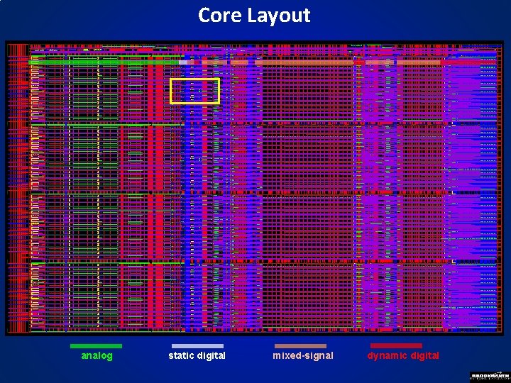
Core Layout analog static digital mixed-signal dynamic digital

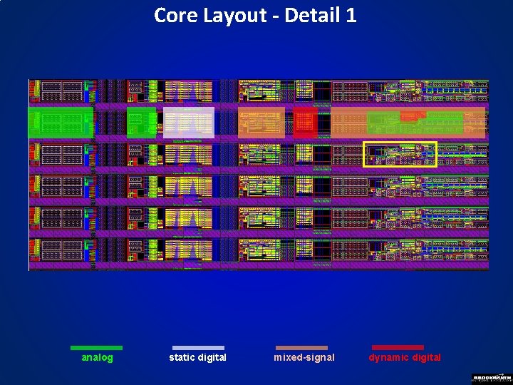
Core Layout - Detail 1 analog static digital mixed-signal dynamic digital

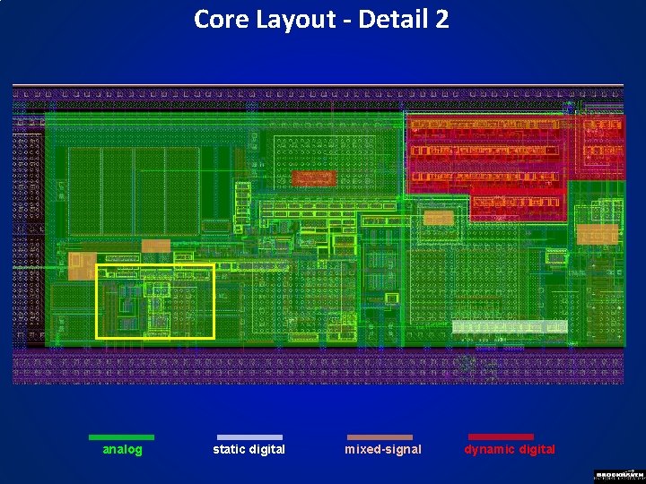
Core Layout - Detail 2 analog static digital mixed-signal dynamic digital

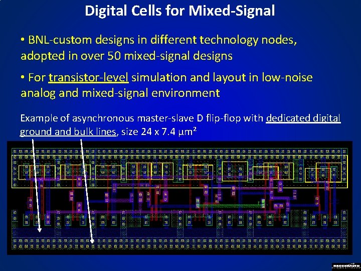
Digital Cells for Mixed-Signal • BNL-custom designs in different technology nodes, adopted in over 50 mixed-signal designs • For transistor-level simulation and layout in low-noise analog and mixed-signal environment Example of asynchronous master-slave D flip-flop with dedicated digital ground and bulk lines, size 24 x 7. 4 µm²

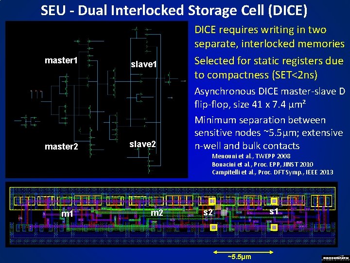
SEU - Dual Interlocked Storage Cell (DICE) master 1 master 2 slave 1 slave 2 DICE requires writing in two separate, interlocked memories Selected for static registers due to compactness (SET<2 ns) Asynchronous DICE master-slave D flip-flop, size 41 x 7. 4 µm² Minimum separation between sensitive nodes ~5. 5µm; extensive n-well and bulk contacts Menouni et al. , TWEPP 2008 Bonacini et al. , Proc. EPP, JINST 2010 Campitelli et al. , Proc. DFT Symp. , IEEE 2013 m 1 m 2 s 1 s 2 ~5. 5µm

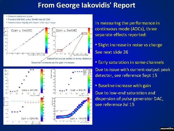
From George Iakovidis' Report In measuring the performance in continuous mode (ADCs), three separate effects reported: • Slight increase in noise vs charge See next slide 26 • Early saturation in some channels Due to issue with current-output peak detector, see reference Sept 15 • Baseline increase with gain Due to low-end saturation and dispersion of pulse generator DAC, see reference Jul 15

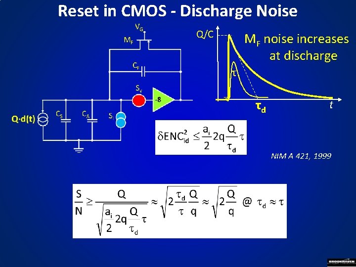
Reset in CMOS - Discharge Noise Q/C MF noise increases at discharge τ τd t NIM A 421, 1999

Answers to John Oliver's Concerns 1/3 1) Subject VMM 2 charge amplifier to simulations which include the s. TGC ion tail currents to demonstrate the rate and amplitude saturation effects. Any deviations of these simulations with s. TGC measurements should be carefully investigated and reconciled. Specifically, reducing the fall time constant using the same circuit topology should be investigated. 2) Repeat this procedure with preamplifier proposed for VMM 3. The results must show non-saturating behavior at expected detector rates with adequate safety margin. Ion tail currents have been investigated, modeled and extensively simulated in VMM 2, and tentatively simulated in VMM 3. See references Dec 14 b, Apr 15 a, and May 15. 3) A traditional solution, used many times, is a simple parallel RC feedback configuration (transimpedance amplifier) with fall time somewhat longer than final shaped peaking time but much shorter than currently exists. Some time should be devoted to see if this topology could be used for VMM 3, as in that case rate limitations should not be a problem. See next slide 30 4) There should be an additional review before submission of VMM 3 to verify that rate limitation problem has been corrected. The front-end revision to accommodate the new requirements is in progress. Extensive simulations will be reported at the next review.

Answers to John Oliver's Concerns 2/3 5) A similar problem exists with respect to abnormally large pulses including those from neutron. This too should be fully simulated. Charges larger than anticipated have been investigated, modeled and simulated in VMM 2, and tentatively simulated in VMM 3. See references Dec 14 b, Apr 15 a, and May 15. According to the new specifications, the expected charge can reach up to 50 p. C (compared to original 2 p. C). A 2% linearity is required for charges up to 2 p. C. A recovery time < 200 ns is required for charges up to 6 p. C. See also https: //edms. cern. ch/document/1536160/1. 6) A specification of noise requirements should be submitted by both MM and s. TGC groups. That requirement should be stated in terms of enc as a function of detector capacitance. Several months ago, VMM 2 noise measurements were presented with no detector or equivalent capacitance connected to front end. These measurements should be repeated with capacitance connected to the front end. This measurement is required to assure that actual device noise meets the specifications for both MM and s. TGC detectors. ENC requirements have been included in the specifications document. Noise measurements vs capacitance of the VMM 1 and VMM 2 front-ends, which are identical, can be found in IEEE Trans. Nucl. Sci. v 60, p. 2314, 2013. Noise simulations of the revised VMM 3 front-end will be presented at the next review.

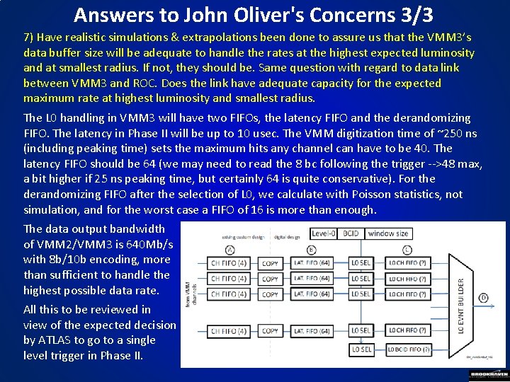
Answers to John Oliver's Concerns 3/3 7) Have realistic simulations & extrapolations been done to assure us that the VMM 3’s data buffer size will be adequate to handle the rates at the highest expected luminosity and at smallest radius. If not, they should be. Same question with regard to data link between VMM 3 and ROC. Does the link have adequate capacity for the expected maximum rate at highest luminosity and smallest radius. The L 0 handling in VMM 3 will have two FIFOs, the latency FIFO and the derandomizing FIFO. The latency in Phase II will be up to 10 usec. The VMM digitization time of ~250 ns (including peaking time) sets the maximum hits any channel can have to be 40. The latency FIFO should be 64 (we may need to read the 8 bc following the trigger -->48 max, a bit higher if 25 ns peaking time, but certainly 64 is quite conservative). For the derandomizing FIFO after the selection of L 0, we calculate with Poisson statistics, not simulation, and for the worst case a FIFO of 16 is more than enough. The data output bandwidth of VMM 2/VMM 3 is 640 Mb/s with 8 b/10 b encoding, more than sufficient to handle the highest possible data rate. All this to be reviewed in view of the expected decision by ATLAS to go to a single level trigger in Phase II.

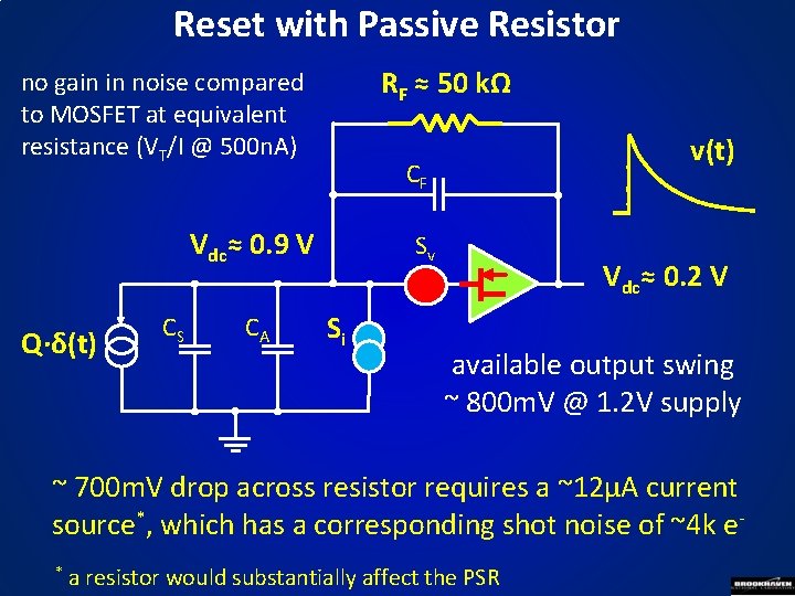
Reset with Passive Resistor RF ≈ 50 kΩ no gain in noise compared to MOSFET at equivalent resistance (VT/I @ 500 n. A) CF Vdc≈ 0. 9 V Q·δ(t) CS CA v(t) Sv Si Vdc≈ 0. 2 V available output swing ~ 800 m. V @ 1. 2 V supply ~ 700 m. V drop across resistor requires a ~12µA current source*, which has a corresponding shot noise of ~4 k e- * a resistor would substantially affect the PSR

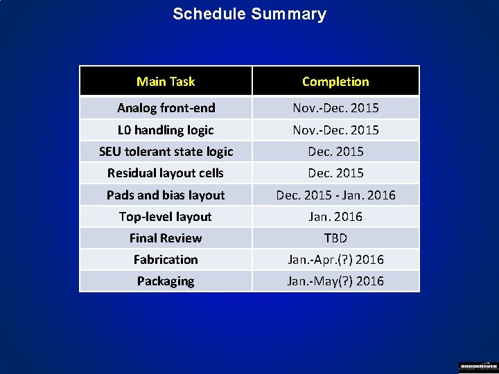
Schedule Summary Main Task Completion Analog front-end Nov. -Dec. 2015 L 0 handling logic Nov. -Dec. 2015 SEU tolerant state logic Dec. 2015 Residual layout cells Dec. 2015 Pads and bias layout Dec. 2015 - Jan. 2016 Top-level layout Jan. 2016 Final Review TBD Fabrication Jan. -Apr. (? ) 2016 Packaging Jan. -May(? ) 2016

Backup Slides

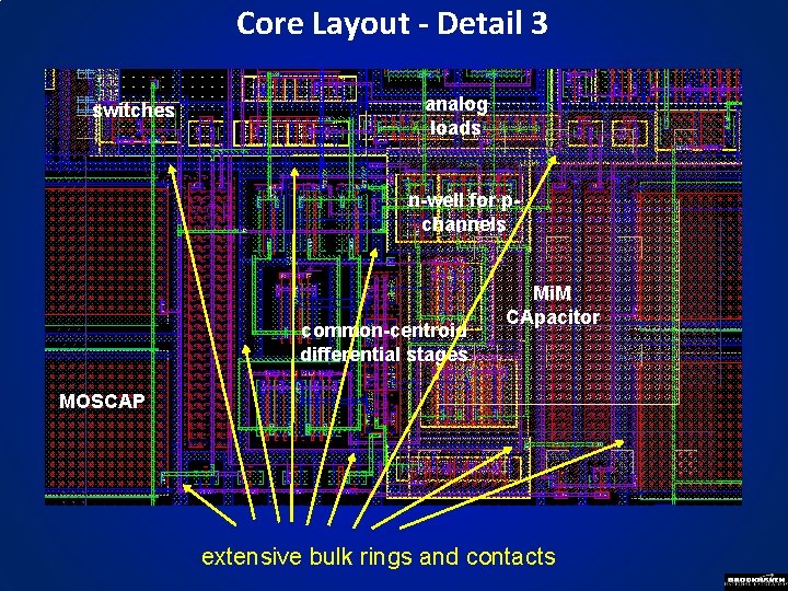
Core Layout - Detail 3 switches analog loads n-well for pchannels common-centroid differential stages Mi. M CApacitor MOSCAP extensive bulk rings and contacts

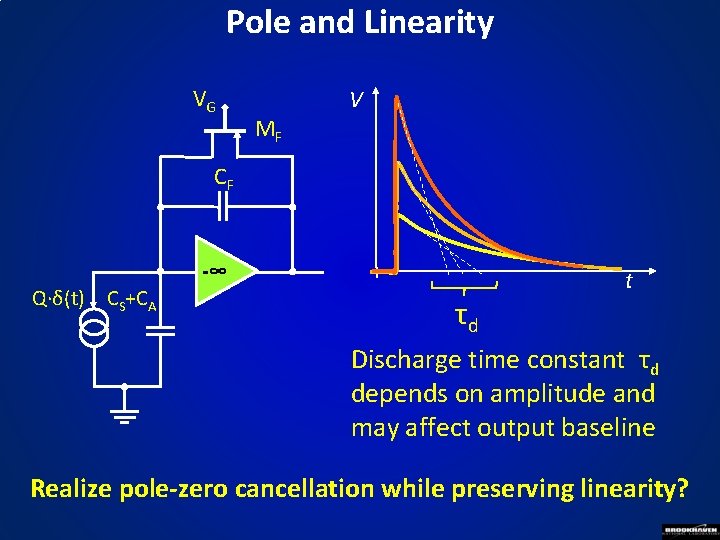
Pole and Linearity VG MF V CF Q·δ(t) -∞ CS+CA τd t Discharge time constant τd depends on amplitude and may affect output baseline Realize pole-zero cancellation while preserving linearity?

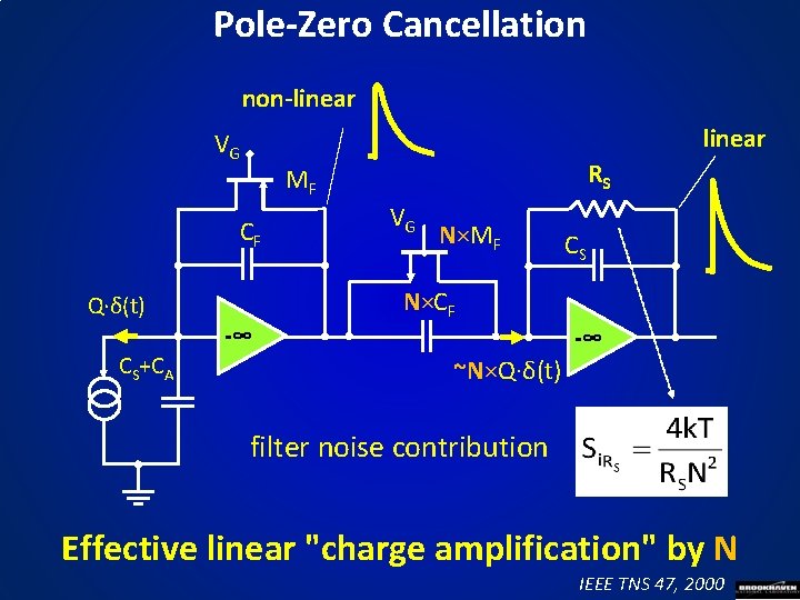
Pole-Zero Cancellation non-linear VG CF Q·δ(t) -∞ CS+CA RS MF VG N×MF CS N×CF -∞ ~N×Q·δ(t) filter noise contribution Effective linear "charge amplification" by N IEEE TNS 47, 2000

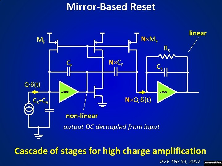
Mirror-Based Reset N×MF MF CF Q·δ(t) linear -∞ CS+CA N×CF RS CS N×Q·δ(t) -∞ non-linear output DC decoupled from input Cascade of stages for high charge amplification IEEE TNS 54, 2007

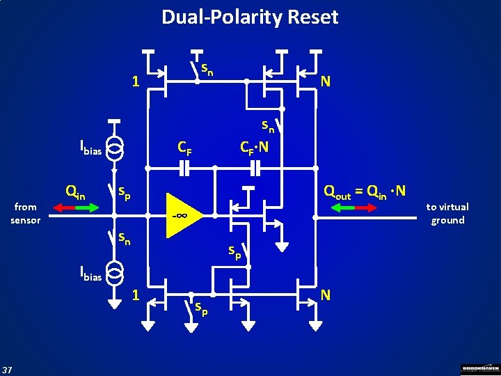
Dual-Polarity Reset sn 1 Ibias from sensor Qin sn CF·N CF sp Qout = Qin ·N -∞ sn sp Ibias 1 37 N sp N to virtual ground