Chapter 2 Logic Simulation Logic Simulation l Purposes
- Slides: 47

電機系 Chapter 2 Logic Simulation 電路邏輯模擬

Logic Simulation l Purposes l l l Verification Debugging Studying design alternative (cost/speed) Computing expected behavior for tests Simulation-based design verification l l l To check correct operations: l e. g. delays of critical paths l free of critical races & oscillation Problem is that tests are hand crafted; Very hard to prove that a test is complete. Formal and assertion-based verification required 2

Modeling for Circuit Simulation l Circuit models l Modeling levels l l l Modeling description (languages) Signal models l l l Behavioral, logic, switch, timing, circuit Logic value models Timing value models Choices of models determine the complexity and accuracy of simulation 3

Level of Circuit Modeling (1/2) l Electronic system level l l Register-Transfer-Level (RTL) l l l Software+hardware Transaction/cycle-accurate functions C/C++, System. C, System. Verilog, etc. Define bit and timing (almost) accurate architecture for sign-off VHDL and Verilog Logic/cell/gate level l Interconnected Boolean gates l l AND, OR, NAND, NOT, XOR, Flip-flops, Transmission gates, buses, etc. Suitable for logic design, verification and test 4

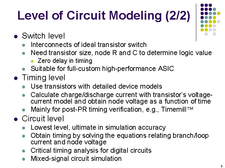
Level of Circuit Modeling (2/2) l Switch level l l Interconnects of ideal transistor switch Need transistor size, node R and C to determine logic value l l l Suitable for full-custom high-performance ASIC Timing level l l Zero delay in timing Use transistors with detailed device models Calculate charge/discharge current with transistor’s voltagecurrent model and obtain node voltage as a function of time Mainly for post-PR timing verification, e. g. , Timemill Circuit level l l Lowest level, ultimate in simulation accuracy Obtain timing by solving the equations relating branch/loop current and node voltage Critical timing analysis for digital circuits Mixed-signal circuit simulation 5

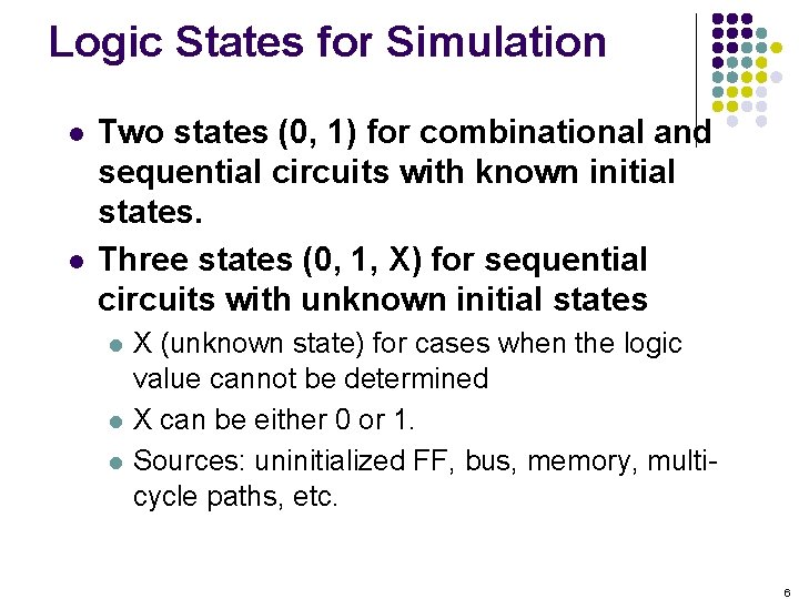
Logic States for Simulation l l Two states (0, 1) for combinational and sequential circuits with known initial states. Three states (0, 1, X) for sequential circuits with unknown initial states l l l X (unknown state) for cases when the logic value cannot be determined X can be either 0 or 1. Sources: uninitialized FF, bus, memory, multicycle paths, etc. 6

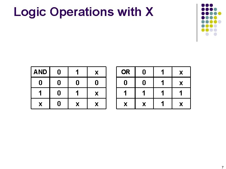
Logic Operations with X AND 0 1 x OR 0 1 x 0 0 0 1 x 1 1 x 0 x x 1 x 7

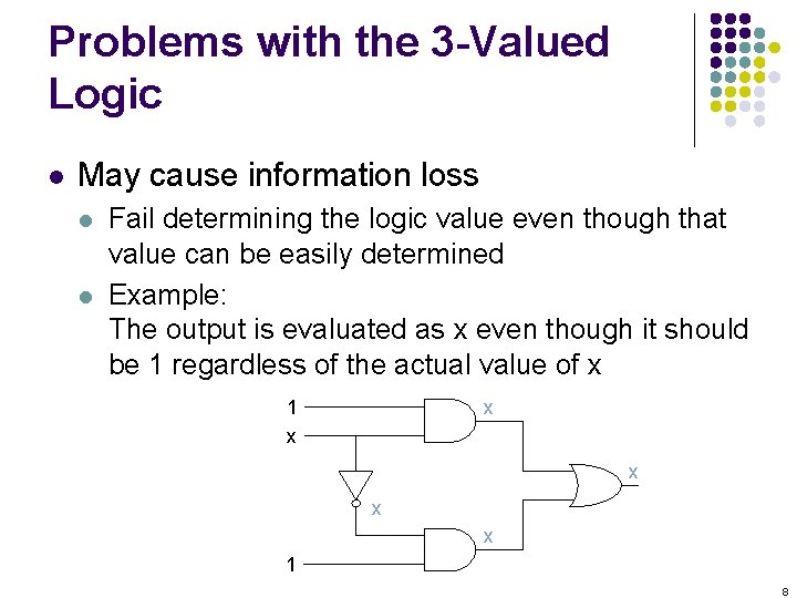
Problems with the 3 -Valued Logic l May cause information loss l l Fail determining the logic value even though that value can be easily determined Example: The output is evaluated as x even though it should be 1 regardless of the actual value of x 1 x x x 1 8

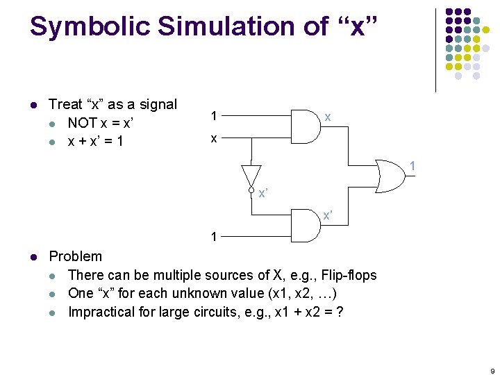
Symbolic Simulation of “x” l Treat “x” as a signal l NOT x = x’ l x + x’ = 1 1 x x 1 x’ x’ 1 l Problem l There can be multiple sources of X, e. g. , Flip-flops l One “x” for each unknown value (x 1, x 2, …) l Impractical for large circuits, e. g. , x 1 + x 2 = ? 9

High-Impedence State Z l Floating state: a node w/o conducting path to either Vdd or Gnd l Logic state of Z is interpreted dynamically l Single floating node l l A set of floating nodes get connected l l Same as its driven value before becoming floating Depends on charge sharing, may become uncertain l A floating node connected to Vdd/Gnd becomes 1/0 l When multiple source drive a floating node, the value depends on the strength of the driving logics. Most MOS circuits containing dynamic logic require four states (0, 1, x, z) for simulation 10

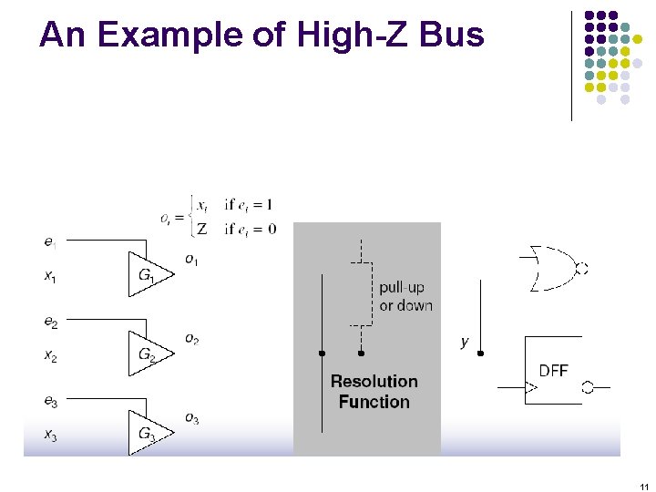
An Example of High-Z Bus 11

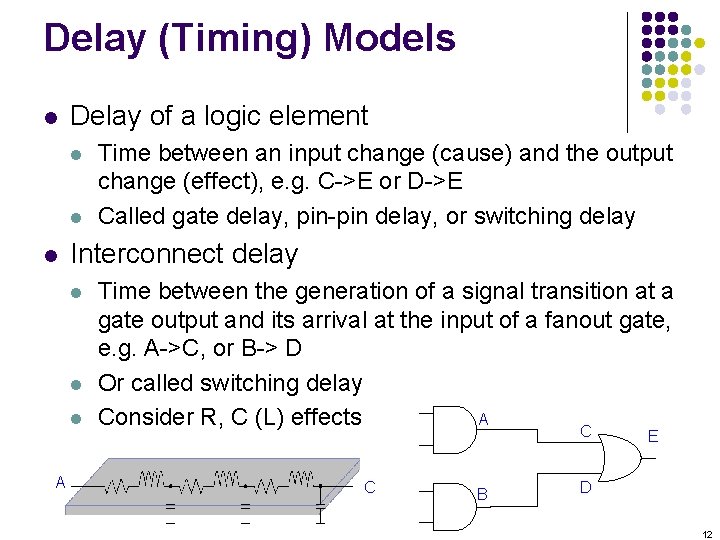
Delay (Timing) Models l Delay of a logic element l l l Interconnect delay l l l A Time between an input change (cause) and the output change (effect), e. g. C->E or D->E Called gate delay, pin-pin delay, or switching delay Time between the generation of a signal transition at a gate output and its arrival at the input of a fanout gate, e. g. A->C, or B-> D Or called switching delay A Consider R, C (L) effects C E C B D 12

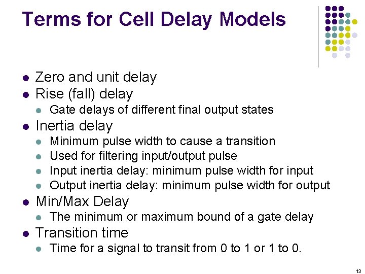
Terms for Cell Delay Models l l Zero and unit delay Rise (fall) delay l l Inertia delay l l l Minimum pulse width to cause a transition Used for filtering input/output pulse Input inertia delay: minimum pulse width for input Output inertia delay: minimum pulse width for output Min/Max Delay l l Gate delays of different final output states The minimum or maximum bound of a gate delay Transition time l Time for a signal to transit from 0 to 1 or 1 to 0. 13

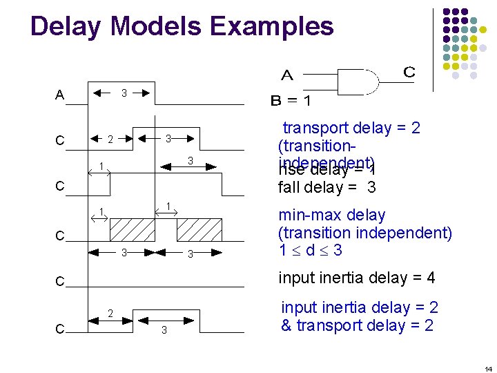
Delay Models Examples 3 A 3 2 C 3 1 C 1 1 C 3 3 min-max delay (transition independent) 1 d 3 input inertia delay = 4 C 2 C transport delay = 2 (transitionindependent) rise delay = 1 fall delay = 3 3 input inertia delay = 2 & transport delay = 2 14

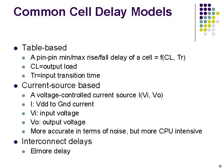
Common Cell Delay Models l Table-based l l Current-source based l l l A pin-pin min/max rise/fall delay of a cell = f(CL, Tr) CL=output load Tr=input transition time A voltage-controlled current source I(Vi, Vo) I: Vdd to Gnd current Vi: input voltage Vo: output voltage More accurate in terms of noise, but more CPU intensive Interconnect delays l Elmore delay 15

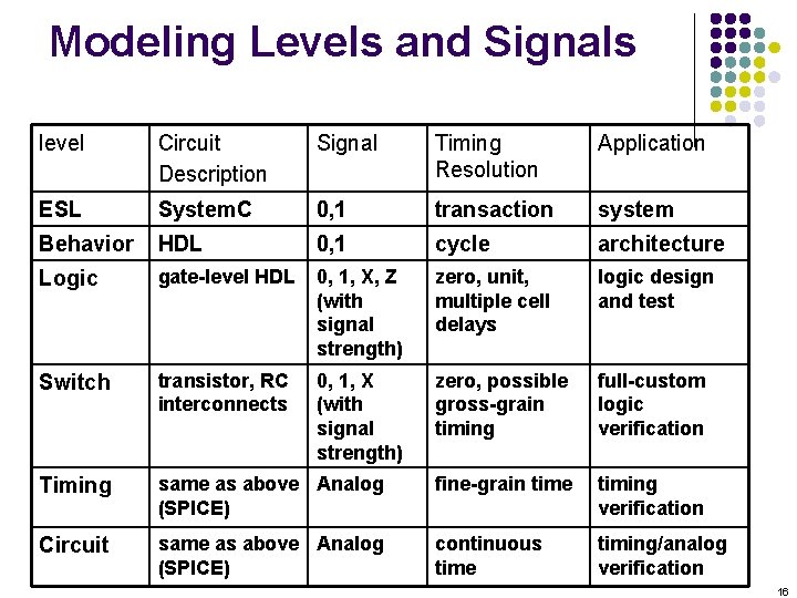
Modeling Levels and Signals level Circuit Description Signal Timing Resolution Application ESL System. C 0, 1 transaction system Behavior HDL 0, 1 cycle architecture Logic gate-level HDL 0, 1, X, Z (with signal strength) zero, unit, multiple cell delays logic design and test Switch transistor, RC interconnects 0, 1, X (with signal strength) zero, possible gross-grain timing full-custom logic verification Timing same as above Analog (SPICE) fine-grain time timing verification Circuit same as above Analog (SPICE) continuous time timing/analog verification 16

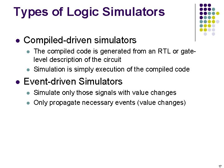
Types of Logic Simulators l Compiled-driven simulators l l l The compiled code is generated from an RTL or gatelevel description of the circuit Simulation is simply execution of the compiled code Event-driven Simulators l l Simulate only those signals with value changes Only propagate necessary events (value changes) 17

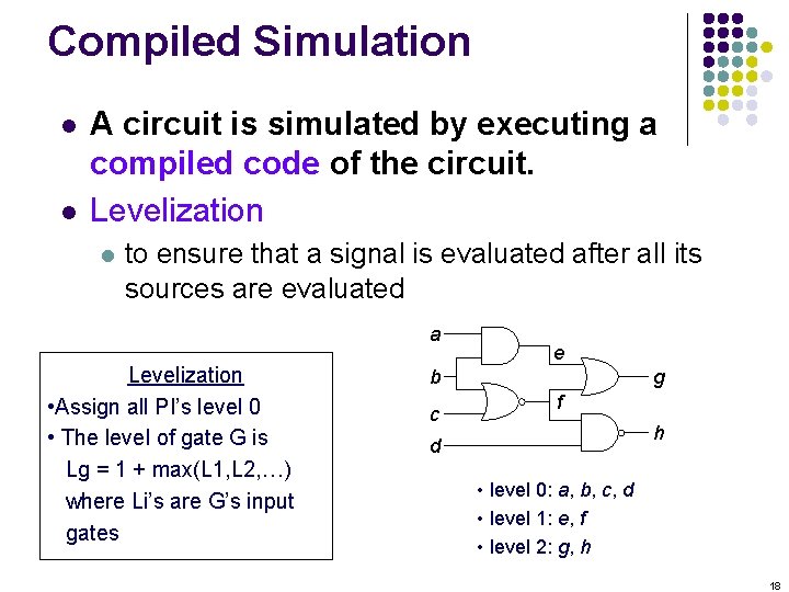
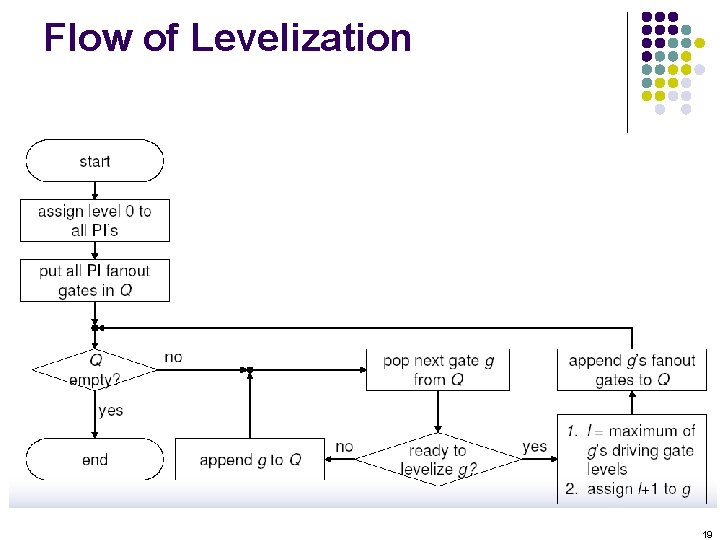
Compiled Simulation l l A circuit is simulated by executing a compiled code of the circuit. Levelization l to ensure that a signal is evaluated after all its sources are evaluated a Levelization • Assign all PI’s level 0 • The level of gate G is Lg = 1 + max(L 1, L 2, …) where Li’s are G’s input gates e b c g f h d • level 0: a, b, c, d • level 1: e, f • level 2: g, h 18

Flow of Levelization 19

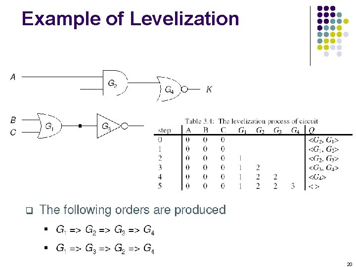
Example of Levelization 20

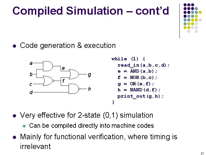
Compiled Simulation – cont’d l Code generation & execution a e b c d l f h Very effective for 2 -state (0, 1) simulation l l g while (1) { read_in(a, b, c, d); e = AND(a, b); f = NOR(b, c); g = OR(e, f); h = NAND(d, f); print_out(g, h); } Can be compiled directly into machine codes Mainly for functional verification, where timing is irrelevant 21

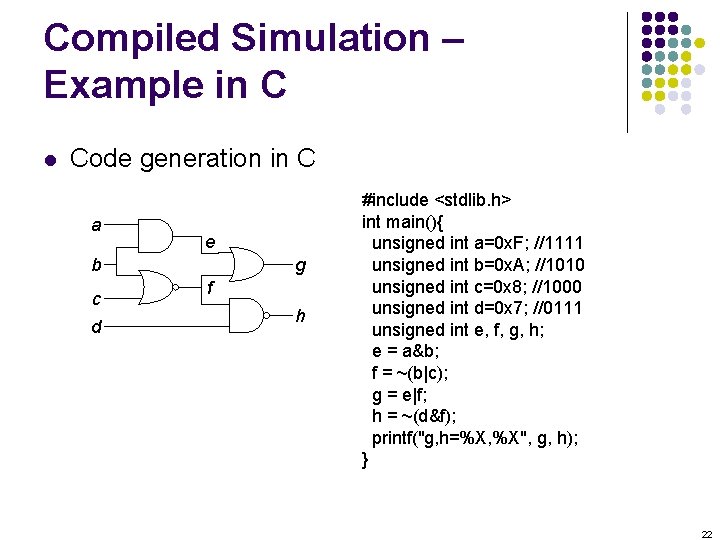
Compiled Simulation – Example in C l Code generation in C a e b c d g f h #include <stdlib. h> int main(){ unsigned int a=0 x. F; //1111 unsigned int b=0 x. A; //1010 unsigned int c=0 x 8; //1000 unsigned int d=0 x 7; //0111 unsigned int e, f, g, h; e = a&b; f = ~(b|c); g = e|f; h = ~(d&f); printf("g, h=%X, %X", g, h); } 22

Problems with Compiled Simulation l Zero-delay model l l Timing problems, e. g. , glitches and races, cannot be modeled Simulation time could be long l Proportional to (input vectors number of gates) l Entire circuit is evaluated even though typically only 1 -10% of signals change at any time l Note RTL compiled simulation is different and fast, since branching can be used. 23

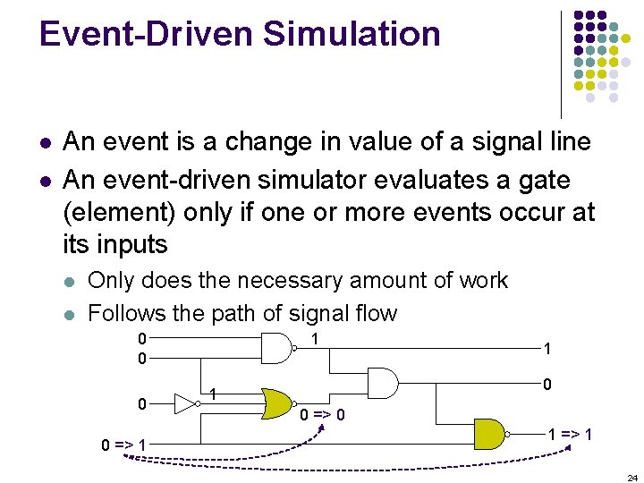
Event-Driven Simulation l l An event is a change in value of a signal line An event-driven simulator evaluates a gate (element) only if one or more events occur at its inputs l l Only does the necessary amount of work Follows the path of signal flow 0 0 => 1 1 1 0 => 0 1 => 1 24

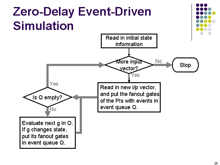
Zero-Delay Event-Driven Simulation Read in initial state information More input vector? No Stop Yes Is Q empty? No Read in new i/p vector, and put the fanout gates of the PIs with events in event queue Q. Evaluate next g in Q. If g changes state, put its fanout gates in event queue Q. 25

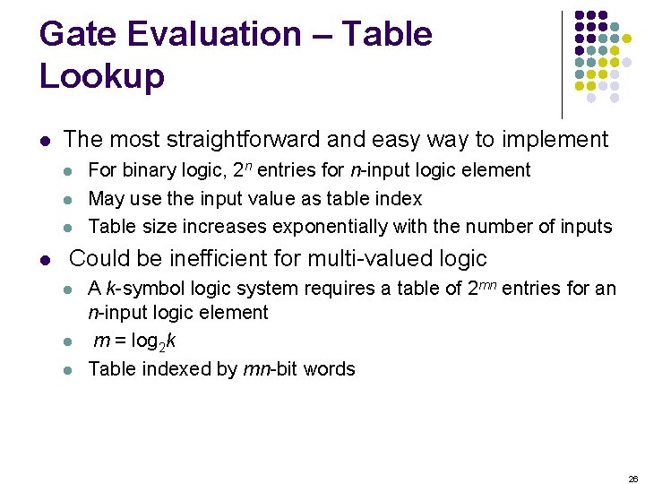
Gate Evaluation – Table Lookup l The most straightforward and easy way to implement l l For binary logic, 2 n entries for n-input logic element May use the input value as table index Table size increases exponentially with the number of inputs Could be inefficient for multi-valued logic l l l A k-symbol logic system requires a table of 2 mn entries for an n-input logic element m = log 2 k Table indexed by mn-bit words 26

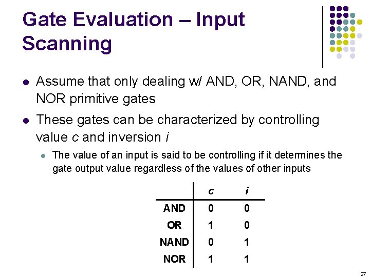
Gate Evaluation – Input Scanning l Assume that only dealing w/ AND, OR, NAND, and NOR primitive gates l These gates can be characterized by controlling value c and inversion i l The value of an input is said to be controlling if it determines the gate output value regardless of the values of other inputs c i AND 0 0 OR 1 0 NAND 0 1 NOR 1 1 27

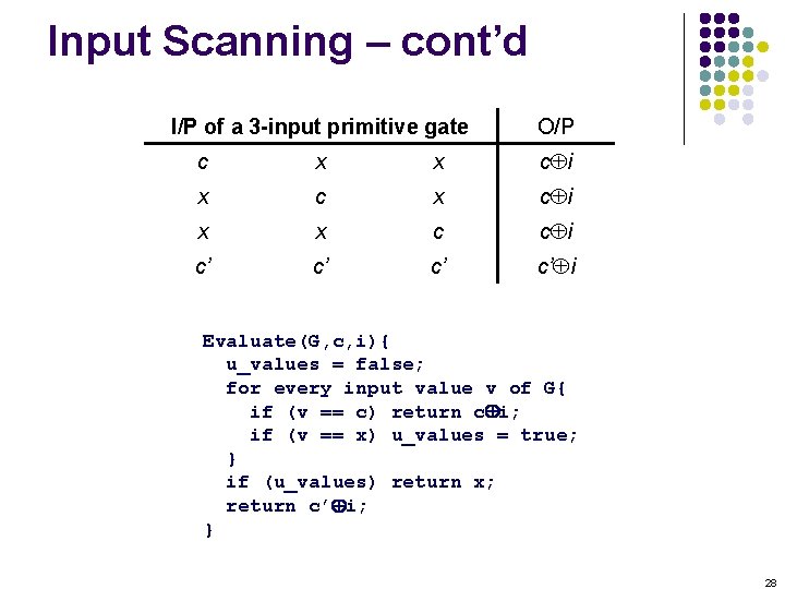
Input Scanning – cont’d I/P of a 3 -input primitive gate O/P c x x c i x x c c i c’ c’ i Evaluate(G, c, i){ u_values = false; for every input value v of G{ if (v == c) return c i; if (v == x) u_values = true; } if (u_values) return x; return c’ i; } 28

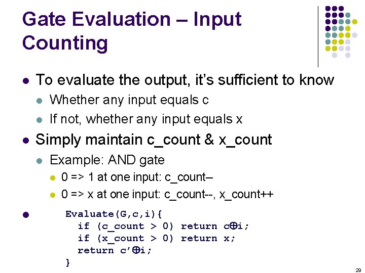
Gate Evaluation – Input Counting l To evaluate the output, it’s sufficient to know l l l Whether any input equals c If not, whether any input equals x Simply maintain c_count & x_count l Example: AND gate l l l 0 => 1 at one input: c_count-0 => x at one input: c_count--, x_count++ Evaluate(G, c, i){ if (c_count > 0) return c i; if (x_count > 0) return x; return c’ i; } 29

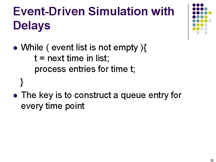
Event-Driven Simulation with Delays While ( event list is not empty ){ t = next time in list; process entries for time t; } l The key is to construct a queue entry for every time point l 30

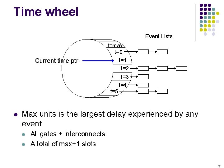
Time wheel Event Lists Current time ptr l t=max t=0 t=1 t=2 t=3 t=4 t=5 Max units is the largest delay experienced by any event l l All gates + interconnects A total of max+1 slots 31

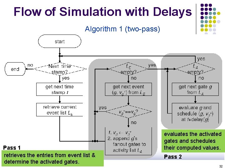
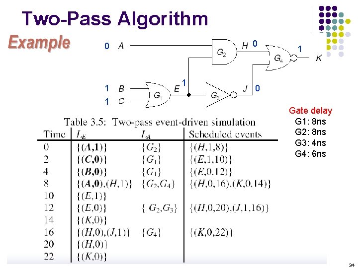
Flow of Simulation with Delays Algorithm 1 (two-pass) Pass 1 retrieves the entries from event list & determine the activated gates. evaluates the activated gates and schedules their computed values. Pass 2 32

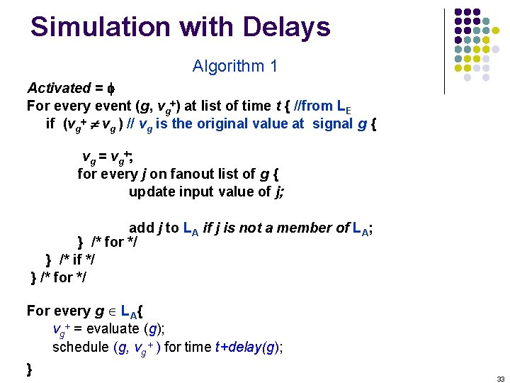
Simulation with Delays Algorithm 1 Activated = f For every event (g, vg+) at list of time t { //from LE if (vg+ vg ) // vg is the original value at signal g { v g = vg + ; for every j on fanout list of g { update input value of j; add j to LA if j is not a member of LA; } /* for */ } /* if */ } /* for */ For every g Î LA{ vg+ = evaluate (g); schedule (g, vg + ) for time t+delay(g); } 33

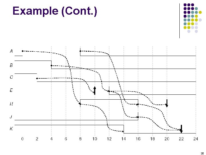
Two-Pass Algorithm 0 0 1 1 0 Gate delay G 1: 8 ns G 2: 8 ns G 3: 4 ns G 4: 6 ns 34

Example (Cont. ) 35

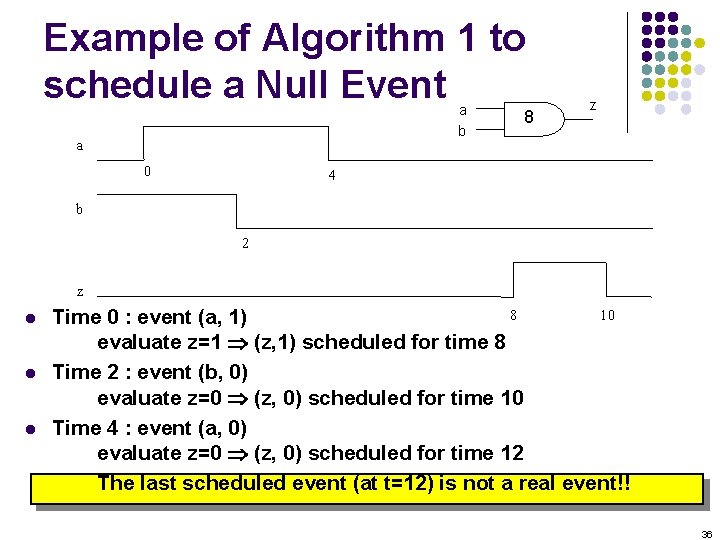
Example of Algorithm 1 to schedule a Null Event a b a 0 8 z 4 b 2 z l l l 8 10 Time 0 : event (a, 1) evaluate z=1 Þ (z, 1) scheduled for time 8 Time 2 : event (b, 0) evaluate z=0 Þ (z, 0) scheduled for time 10 Time 4 : event (a, 0) evaluate z=0 Þ (z, 0) scheduled for time 12 The last scheduled event (at t=12) is not a real event!! 36

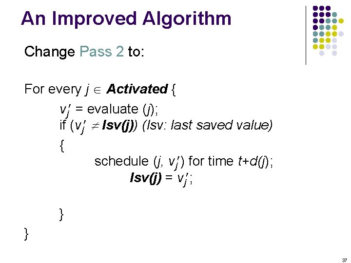
An Improved Algorithm Change Pass 2 to: For every j Î Activated { vj¢ = evaluate (j); if (vj¢ lsv(j)) (lsv: last saved value) { schedule (j, vj¢) for time t+d(j); lsv(j) = vj¢; } } 37

Two Pass V. S. One Pass Algorithm l Two-pass strategy performs the evaluations only after all the concurrent events have been retrieved l l l to avoid repeated evaluations of gates having multiple input changes. Experience shows, however, that most gates are evaluated as a result of only one input change. One-pass strategy: l l Evaluates a gate as soon as it is activated Avoids the overhead of building the Activated set 38

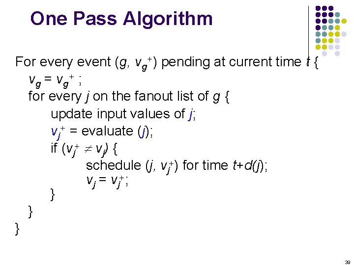
One Pass Algorithm For every event (g, vg+) pending at current time t { vg = vg+ ; for every j on the fanout list of g { update input values of j; vj+ = evaluate (j); if (vj+ vj) { schedule (j, vj+) for time t+d(j); vj = vj+; } } } 39

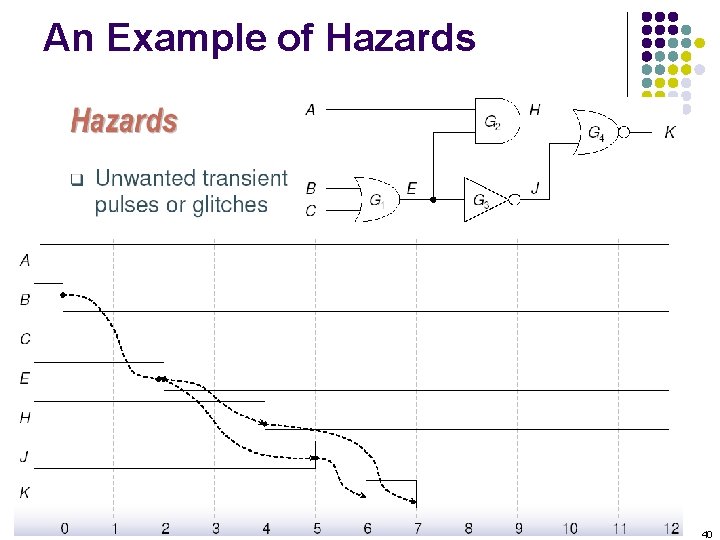
An Example of Hazards 40

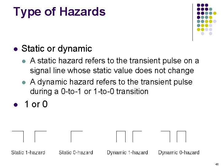
Type of Hazards l Static or dynamic l l l A static hazard refers to the transient pulse on a signal line whose static value does not change A dynamic hazard refers to the transient pulse during a 0 -to-1 or 1 -to-0 transition 1 or 0 41

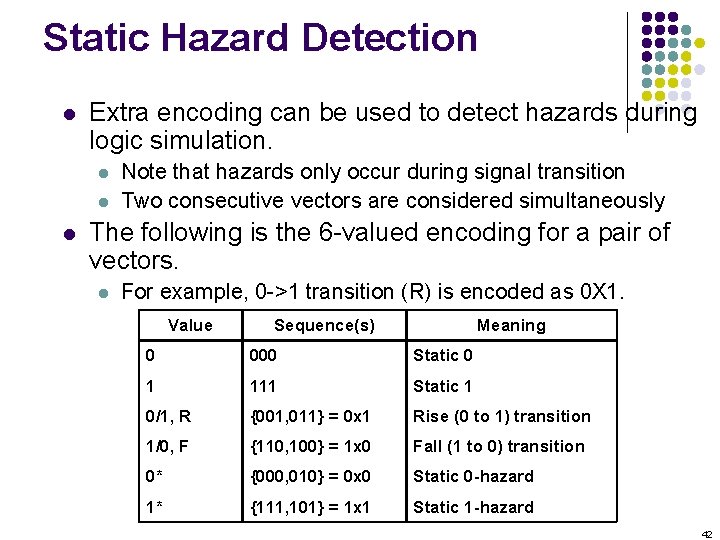
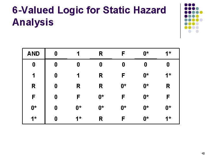
Static Hazard Detection l Extra encoding can be used to detect hazards during logic simulation. l l l Note that hazards only occur during signal transition Two consecutive vectors are considered simultaneously The following is the 6 -valued encoding for a pair of vectors. l For example, 0 ->1 transition (R) is encoded as 0 X 1. Value Sequence(s) Meaning 0 000 Static 0 1 111 Static 1 0/1, R {001, 011} = 0 x 1 Rise (0 to 1) transition 1/0, F {110, 100} = 1 x 0 Fall (1 to 0) transition 0* {000, 010} = 0 x 0 Static 0 -hazard 1* {111, 101} = 1 x 1 Static 1 -hazard 42

6 -Valued Logic for Static Hazard Analysis AND 0 1 R F 0* 1* 0 0 0 0 1 R F 0* 1* R 0 R R 0* 0* R F 0* 0 0* 0* 0* 1* 0 1* R F 0* 1* 43

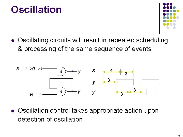
Oscillation l Oscillating circuits will result in repeated scheduling & processing of the same sequence of events S = 1=>0=>1 3 y y R=1 l 3 y’ 4 S y’ 3 3 Oscillation control takes appropriate action upon detection of oscillation 44

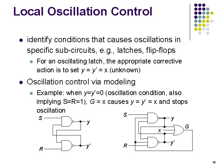
Local Oscillation Control l identify conditions that causes oscillations in specific sub-circuits, e. g. , latches, flip-flops l l For an oscillating latch, the appropriate corrective action is to set y = y’ = x (unknown) Oscillation control via modeling l Example: when y=y’=0 (oscillation condition, also implying S=R=1), G = x causes y = y’ = x and stops oscillation S S y y G x R y’ 45

Global Oscillation Control l Detection of global oscillation is computationally infeasible l l Requires detecting cyclic sequences of values for any signal in the circuit A typical procedure is to count the number of events occurring after any primary input change l Oscillation is “assumed” if the number exceeds the specified limit 46

Simulation Engines l Motivation l l Simulation engines are special-purpose hardware for speeding up logic simulation. l l l Logic simulation is time consuming. Usually attached to a general-purpose host computer through, for example, VME/PCI bus. FPGA-based logic emulation Use parallel and/or distributed processing architectures. 47