ActiveMode Leakage Reduction with DataRetained Power Gating Andrew



- Slides: 16

Active-Mode Leakage Reduction with Data-Retained Power Gating Andrew B. Kahng†, Seokhyeong Kang† and Bongil Park* †UC San Diego, *Samsung Electronics

Outline • Background and Motivation • Data-Retained Power Gating – Integrated Clock and Power Gating – Flip-flop implementation • Experimental Results • Conclusions and Ongoing Work 25 -Oct-21 VLSI CAD Laboratory / UC San Diego 1

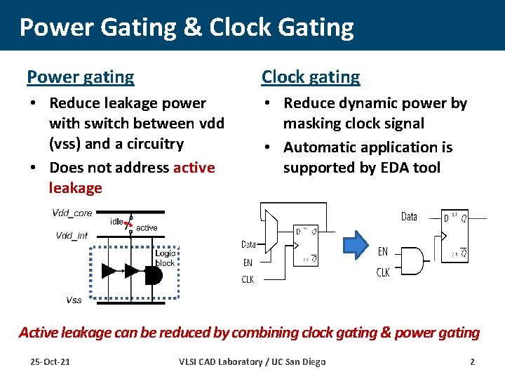
Power Gating & Clock Gating Power gating Clock gating • Reduce leakage power with switch between vdd (vss) and a circuitry • Does not address active leakage • Reduce dynamic power by masking clock signal • Automatic application is supported by EDA tool Active leakage can be reduced by combining clock gating & power gating 25 -Oct-21 VLSI CAD Laboratory / UC San Diego 2

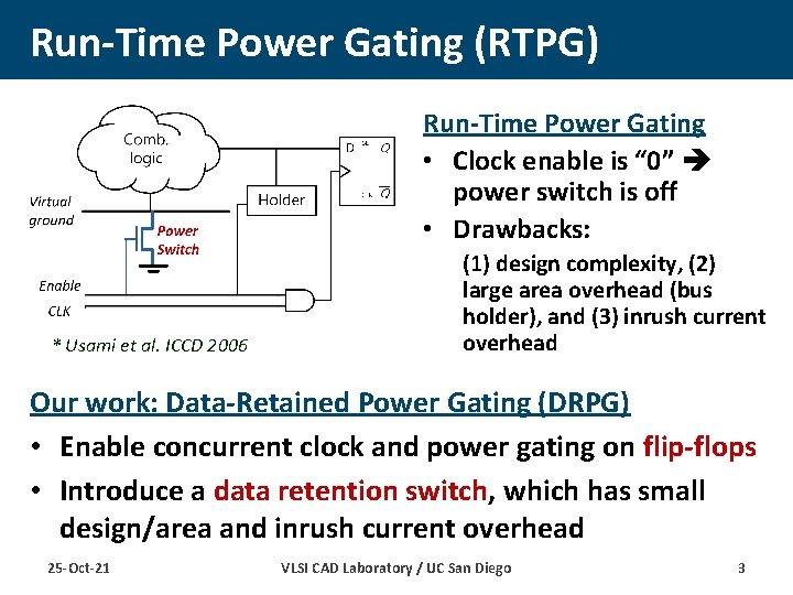
Run-Time Power Gating (RTPG) Run-Time Power Gating • Clock enable is “ 0” power switch is off • Drawbacks: * Usami et al. ICCD 2006 (1) design complexity, (2) large area overhead (bus holder), and (3) inrush current overhead Our work: Data-Retained Power Gating (DRPG) • Enable concurrent clock and power gating on flip-flops • Introduce a data retention switch, which has small design/area and inrush current overhead 25 -Oct-21 VLSI CAD Laboratory / UC San Diego 3

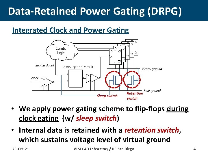
Data-Retained Power Gating (DRPG) Integrated Clock and Power Gating • We apply power gating scheme to flip-flops during clock gating (w/ sleep switch) • Internal data is retained with a retention switch, which sustains voltage level of virtual ground 25 -Oct-21 VLSI CAD Laboratory / UC San Diego 4

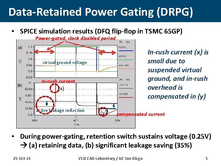
Data-Retained Power Gating (DRPG) • SPICE simulation results (DFQ flip-flop in TSMC 65 GP) Power-gated, clock disabled period (a) In-rush current (x) is small due to suspended virtual ground, and in-rush overhead is compensated in (y) virtual ground voltage (b) in-rush current (x) active leakage reduction (y) compensated current • During power-gating, retention switch sustains voltage (0. 25 V) (a) retaining data, (b) significant leakage saving (35%) 25 -Oct-21 VLSI CAD Laboratory / UC San Diego 5

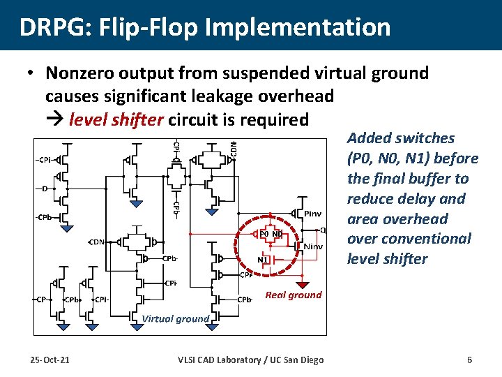
DRPG: Flip-Flop Implementation • Nonzero output from suspended virtual ground causes significant leakage overhead level shifter circuit is required Added switches (P 0, N 1) before the final buffer to reduce delay and area overhead over conventional level shifter 25 -Oct-21 VLSI CAD Laboratory / UC San Diego 6

Physical Implementation • Implementation with a global power gating – Three modes (static leakage saving, active leakage saving and normal operation) are available • Standard cell implementation for a multi-bit flip-flop – Include sleep and retention switch inside the standard cell PGEN: global power gating enable CKEN: clock enable signal 25 -Oct-21 VLSI CAD Laboratory / UC San Diego 7

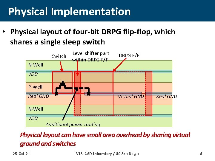
Physical Implementation • Physical layout of four-bit DRPG flip-flop, which shares a single sleep switch Switch N-Well Level shifter part within DRPG F/F VDD P-Well Real GND Virtual GND Real GND N-Well VDD Additional power routing Physical layout can have small area overhead by sharing virtual ground and switches 25 -Oct-21 VLSI CAD Laboratory / UC San Diego 8

Outline • Background and Motivation • Data-Retained Power Gating – Integrated Clock and Power Gating – Flip-flop implementation • Experimental Results • Conclusions and Ongoing Work 25 -Oct-21 VLSI CAD Laboratory / UC San Diego 9

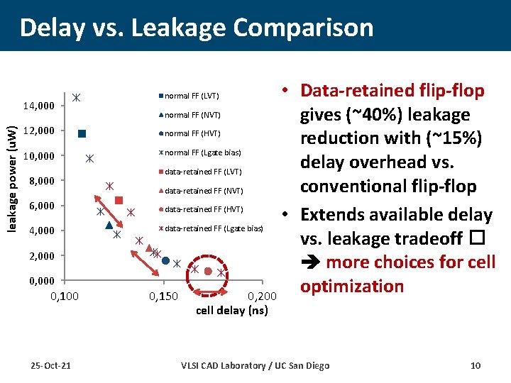
Delay vs. Leakage Comparison leakage power (u. W) 14, 000 12, 000 10, 000 8, 000 6, 000 4, 000 2, 000 0, 100 25 -Oct-21 • Data-retained flip-flop normal FF (NVT) gives (~40%) leakage normal FF (HVT) reduction with (~15%) normal FF (Lgate bias) delay overhead vs. data-retained FF (LVT) conventional flip-flop data-retained FF (NVT) data-retained FF (HVT) • Extends available delay data-retained FF (Lgate bias) vs. leakage tradeoff � more choices for cell optimization 0, 150 0, 200 normal FF (LVT) cell delay (ns) VLSI CAD Laboratory / UC San Diego 10

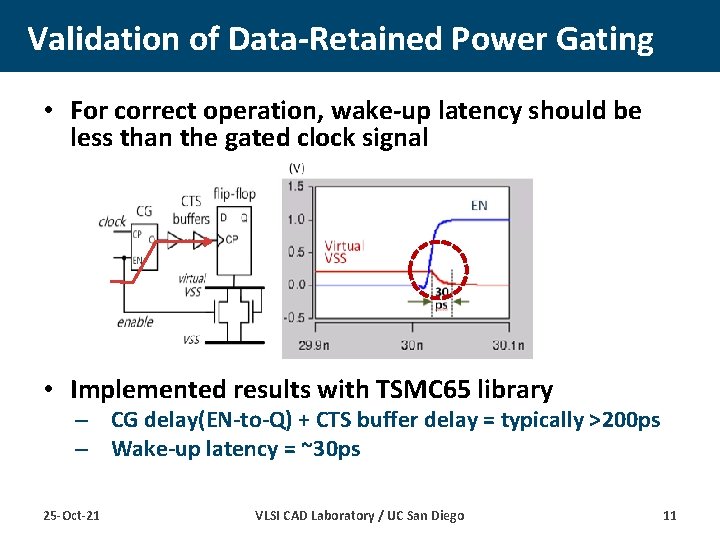
Validation of Data-Retained Power Gating • For correct operation, wake-up latency should be less than the gated clock signal • Implemented results with TSMC 65 library – CG delay(EN-to-Q) + CTS buffer delay = typically >200 ps – Wake-up latency = ~30 ps 25 -Oct-21 VLSI CAD Laboratory / UC San Diego 11

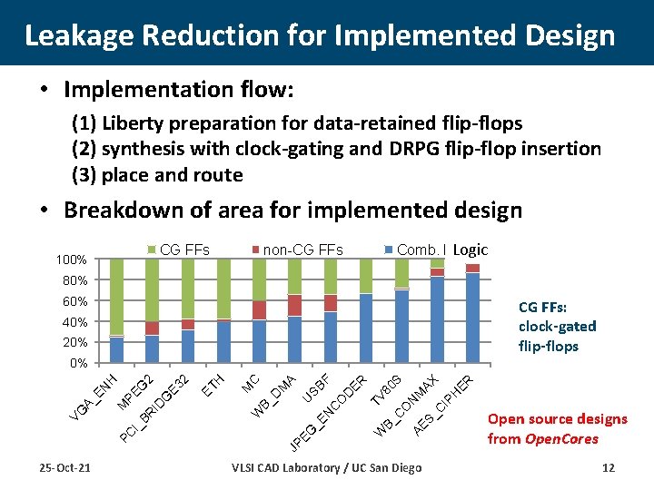
Leakage Reduction for Implemented Design • Implementation flow: (1) Liberty preparation for data-retained flip-flops (2) synthesis with clock-gating and DRPG flip-flop insertion (3) place and route • Breakdown of area for implemented design CG FFs 100% Comb. logics Logic non-CG FFs 80% 60% CG FFs: clock-gated flip-flops 40% 20% AE VLSI CAD Laboratory / UC San Diego ER H IP S_ C O N M AX 80 S C TV B_ D O C U _E N EG JP W ER F SB A B_ D M C M W ET H 2 E 3 G BR I_ PC 25 -Oct-21 ID PE M VG A_ EN H G 2 0% Open source designs from Open. Cores 12

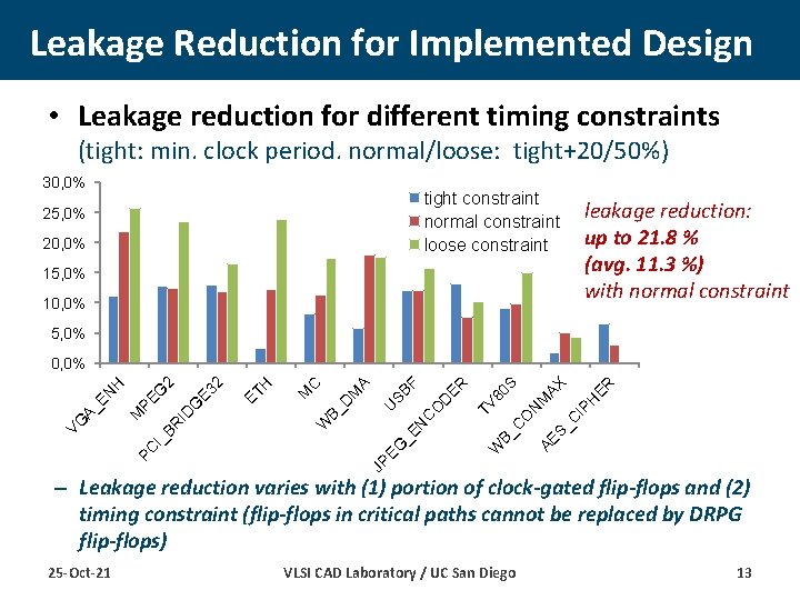
Leakage Reduction for Implemented Design • Leakage reduction for different timing constraints (tight: min. clock period. normal/loose: tight+20/50%) 30, 0% tight constraint normal constraint loose constraint 25, 0% 20, 0% leakage reduction: up to 21. 8 % (avg. 11. 3 %) with normal constraint 15, 0% 10, 0% 5, 0% ER C S_ AE B_ C O N IP H M AX 80 S TV D O C _E N EG W ER F SB D B_ U M A C W 2 ET H M JP PC I_ BR ID G E 3 G PE M VG A_ EN H 2 0, 0% – Leakage reduction varies with (1) portion of clock-gated flip-flops and (2) timing constraint (flip-flops in critical paths cannot be replaced by DRPG flip-flops) 25 -Oct-21 VLSI CAD Laboratory / UC San Diego 13

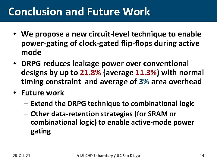
Conclusion and Future Work • We propose a new circuit-level technique to enable power-gating of clock-gated flip-flops during active mode • DRPG reduces leakage power over conventional designs by up to 21. 8% (average 11. 3%) with normal timing constraint and average of 3% area overhead • Future work – Extend the DRPG technique to combinational logic – Other data-retention strategies (for SRAM or combinational logic) to enable active-mode power gating 25 -Oct-21 VLSI CAD Laboratory / UC San Diego 14

Thank you 25 -Oct-21 VLSI CAD Laboratory / UC San Diego 15