1 Clock skew and signal reflection kyungee kaist


 maximum allowable clock skew = tskew, max(Race equation) to prevent race condition,")

 Race condition: double-sided constraint on clock width, tclk-width – clock width must")


 and delay condition( on")
 routing clock in the opposite direction")
 at")
")
 i) Loop filter : – loop filter")

 Chip-to-chip clock skew due to global")
")
 Divide")

 equal-length chip-to-chip interconnection 2) PLL-based clock generator/buffer, and")
 - H-tree is better than X-tree")


: When")
 of interconnection line : 1) From")
 From lossy transmission line RC model : Eq. (1), (2) need to")


- Slides: 32
1 Clock skew and signal reflection 경종민 kyung@ee. kaist. ac. kr
2 1. Clocking Schemes based on each storage element • Waveforms for D-latch, +ve edge-triggered D-f/f, and 2 phase double latch(latter two are equivalent to each other)
3 Finite State Machines based on each storage element Clk 1 and clk 2 are non-overlapping each other
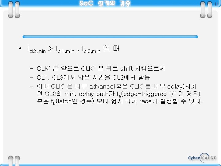
• Clock skew 4 positive skew negative skew signal direction clk CL 1 2 clk’ +ve clk’ -ve – Positive skew tdelay, min must be obeyed. Otherwise, 2 nd f/f, at the current sample point, samples the next value, not the current one (which is the correct one). called double clocking – Negative skew Tp-(tdelay, max + tsetup) must be obeyed. Otherwise, 2 nd f/f, at the next sample point, samples the old value, not the updated value(which is the correct one).
5 • Single-phase system with edge-triggered flipflops negative skew의 경우임
6 i) maximum allowable clock skew = tskew, max(Race equation) to prevent race condition, i. e. , to prevent f/f from deciding Q with next input rather than current input. tskew, max < tf/f, min+tcl, min- thold, max (thold: min. time a signal needs to stay stable after clock edge) ii) min. clock cycle time for correct operation with stable f/f inputs considering clock skew(Delay equation) Tp, min>tf/f, max+tcl. max+tsetup, max- tskew, max iii) tclk-width>thold, to guarantee correct data capture.
7 • Single-phase system with latches - ve skew의 경우임
8 i) Race condition: double-sided constraint on clock width, tclk-width – clock width must be greater than tsetup. ( tsetup for latch is the min. time a signal should remain stable before the fall of clock edge) tclk-width tsetup, max – clock width must be shorter than the sum of 1 -stage delay(consisting of tlatch and tcl) minus hold time and skew, to prevent any signal from passing through more than one stage. Tclk-width tlatch, min + tcl, min - thold, max - tskew, max ii) min. cycle time(in the critical stage) tcycle, min > tlatch, max + tcl, max + tsetup, max + tskew, max- tclk-width, min – some delay as much as this can be transferred to the preceding or succeeding non-critical stages.
9 • 2 -phase non-overlapping clock using double latchl
10 • Intentional clock skew
12 • Relation between race condition( on max, clock skew) and delay condition( on min. clock period) i) when data & clk are running in the same direction(positive skew) • Clock skew should be tightly controlled to prevent race condition. • With +ve skew, clock frequency can be increased for higher performance. ii) when data and clock are running in opposite direction(negative skew) • No need to worry about race condition, • But, -ve skew degrades the performance by increasing the min. clock period according to the delay equation.
13 • How to suppress race condition 1) routing clock in the opposite direction of data(easy to implement in datapath) • at the cost of performance degradation 2) controlling the non-overlap periods of clock( in 2 -phase clocking) 3) Try to obtain good clock distribution network to obtain as uniform clock skew as possible at the local clock point. ( Absolute skew between clock source and local clock point is irrelevant) 4) Clock dist. Network • • • interconnect material shape of the dist. Network clock driver/buffering schemes load, i. e. , fan-out on the clock lines rise/fall time of the clock 5) Avoid global clock/ Use self-timed approach
2. Clock Distribution Network • H-tree as clock dist. Network – clock receiver(photo-diode) at the center receiving sharp laser pulse through a glass window in the package 14
15 • Two-level buffering(Hierarchy)
16 • Composition of a PLL(Phase-Locked Loop) i) Loop filter : – loop filter is introduced to remove clock jitter. – 1 st to 3 rd-order LPF is generally needed, as excessive phase shift due to high-order filtering can cause instability in this feedback structure. ii) Lock range : range of input frequency over which output follows input with given relationship. iii) Lock time : time for PLL to lock into the input iv) Jitter : Loop filter(LPF) helps remove jitter.
17 • How to minimize clock skew in multi-chip system, i. e. , board or multiple-board system. Global Clock Source i) Global dist. Network. ii) On-chip clock generator/buffer; PLL can help here only. iii) Local dist. Network.
18 • Each Component of Skew : i) Chip-to-chip clock skew due to global dist. Network ; can be suppressed by ; – placing clock pins/pads at the identical positions on the chip carrier/chip. – Keeping the lead length and capacitive loading of clock pins and wires from the global clock source to each clock pin as identical as possible. ii) Skew due to on-chip clock generator/buffer can be suppressed by PLL;
19 • Each Component of PLL(Phase detector, LPF, voltage-controlled delay line)
20 • Methodology for dealing with timing problems in LARGE systems ; 1) Divide the whole system into a number of regions, with each region operating in synchronous manner. 2) Communication among each region is either i) through a global clock slower( N) than local clock or ii) asynchronously using self-timed discipline.
• Using PLL for local synchronization between global & local clocks. Delay of local clock is adjusted via. PLL to make the local clock edge occurring simultaneously with global clock edge. 21
22 • Minimal skew system 1) equal-length chip-to-chip interconnection 2) PLL-based clock generator/buffer, and 3) equal-length on-chip distribution(H-tree)
23 • Symmetric clock trees(H- vs X- tree) - H-tree is better than X-tree in that i) in H-tree, no corners sharper than 90 , thus with smaller inductive discontinuity, reflection is small. ii) in H-tree, fan-out is only 2, simplifying impedance matching
24 • Reduction of inductive discontinuities at the corners of H-tree.
25 • Matching condition at the branch point : Zk+1 Zk Zk+1 - impedance matching occurs when Zk=Zk+1//Zk+1= Zk+1 2
26 • Driving the clock lines :
• Sharpening clock signal at the receiver front before distribution in the subblock using schmitt trigger or source-end-terminated buffer. (Look at sharp rise of Vb in previous slide. ) 27
• RC network representation of H-clock tree(simplified as a distributed RC line): When tailored H-clock tree is used, I. e. , if the line width is halved at each branching point, above distributed RC tree network is equivalent to a uniformly distributed RC line. (R 1= R 2= R 3=…, C 1=2 C 2=4 C 3=. . . ) 28
29 • Requirement of the cross-sectional geometry(height, width) of interconnection line : 1) From distributed RC model ; – Total distance from clock source to end point(ltot) in H-tree : – Time required for the last node to reach 90% of its final value : Rint : resistance of interconnection per unit length Cint : capacitance per unit length
30 2) From lossy transmission line RC model : Eq. (1), (2) need to be considered in determining H&W. For high frequency, skin effect prevents thickening the interconnection by more than 2 -4 times the skin depth ineffective. For 1 GHz, skin depth of aluminum is 2. 8 m.
31 • Simulation of H-clock tree with the last stage unmatched.
32 • Reflections in the final unmatched branch :