XRay Photoelectron Spectroscopy XPS www nano 4 me





- Slides: 36

X-Ray Photoelectron Spectroscopy (XPS) www. nano 4 me. org © 2018 The Pennsylvania State University XPS 1

Outline Ø Basic principles Ø Instrumentation Ø Peak characteristics Ø Quantitative analysis Ø Depth profiling www. nano 4 me. org © 2018 The Pennsylvania State University XPS 2

X-Ray Photoelectron Spectroscopy (XPS) Ø X-ray Photoelectron Spectroscopy (XPS), also known as Electron Spectroscopy for Chemical Analysis (ESCA), is used to determine quantitative atomic composition and chemistry. Ø A sample is irradiated with monochromatic x-rays, resulting in the emission of photoelectrons whose energies are characteristic of the elements within the sampling volume. Ø An XPS spectra is created by plotting the number of electrons verses their binding energy. www. nano 4 me. org © 2018 The Pennsylvania State University XPS 3

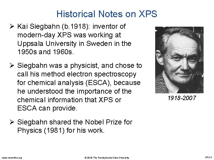
Historical Notes on XPS Ø Kai Siegbahn (b. 1918): inventor of modern-day XPS was working at Uppsala University in Sweden in the 1950 s and 1960 s. Ø Siegbahn was a physicist, and chose to call his method electron spectroscopy for chemical analysis (ESCA), because he understood the importance of the chemical information that XPS or ESCA can provide. 1918 -2007 Ø Siegbahn shared the Nobel Prize for Physics (1981) for his work. www. nano 4 me. org © 2018 The Pennsylvania State University XPS 4

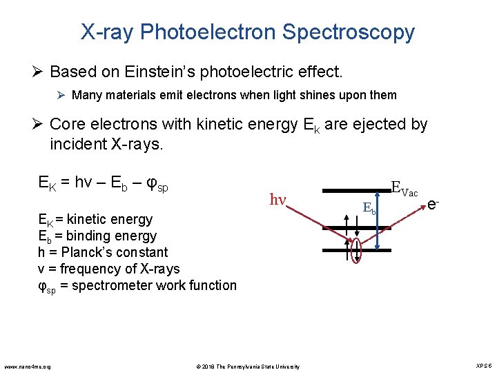
X-ray Photoelectron Spectroscopy Ø Based on Einstein’s photoelectric effect. Ø Many materials emit electrons when light shines upon them Ø Core electrons with kinetic energy Ek are ejected by incident X-rays. EK = hν – Eb – φsp hν EK = kinetic energy Eb = binding energy h = Planck’s constant ν = frequency of X-rays φsp = spectrometer work function www. nano 4 me. org © 2018 The Pennsylvania State University EVac Eb e- XPS 5

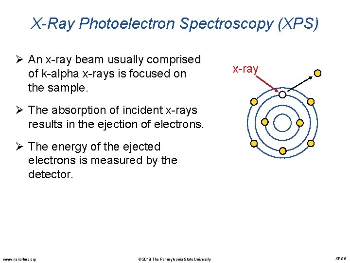
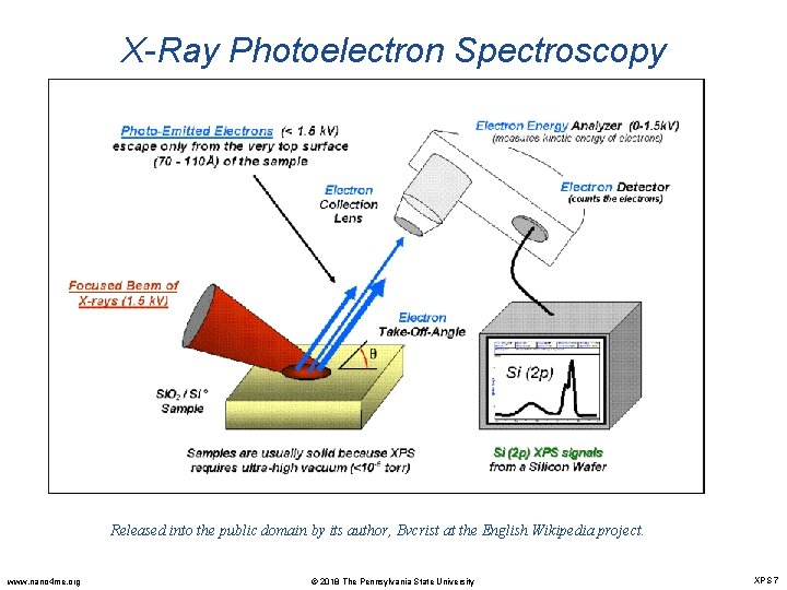
X-Ray Photoelectron Spectroscopy (XPS) Ø An x-ray beam usually comprised of k-alpha x-rays is focused on the sample. x-ray Ø The absorption of incident x-rays results in the ejection of electrons. Ø The energy of the ejected electrons is measured by the detector. www. nano 4 me. org © 2018 The Pennsylvania State University XPS 6

X-Ray Photoelectron Spectroscopy Released into the public domain by its author, Bvcrist at the English Wikipedia project. www. nano 4 me. org © 2018 The Pennsylvania State University XPS 7

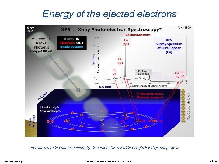
Energy of the ejected electrons Released into the public domain by its author, Bvcrist at the English Wikipedia project. www. nano 4 me. org © 2018 The Pennsylvania State University XPS 8

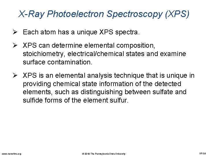
X-Ray Photoelectron Spectroscopy (XPS) Ø Each atom has a unique XPS spectra. Ø XPS can determine elemental composition, stoichiometry, electrical/chemical states and examine surface contamination. Ø XPS is an elemental analysis technique that is unique in providing chemical state information of the detected elements, such as distinguishing between sulfate and sulfide forms of the element sulfur. www. nano 4 me. org © 2018 The Pennsylvania State University XPS 9

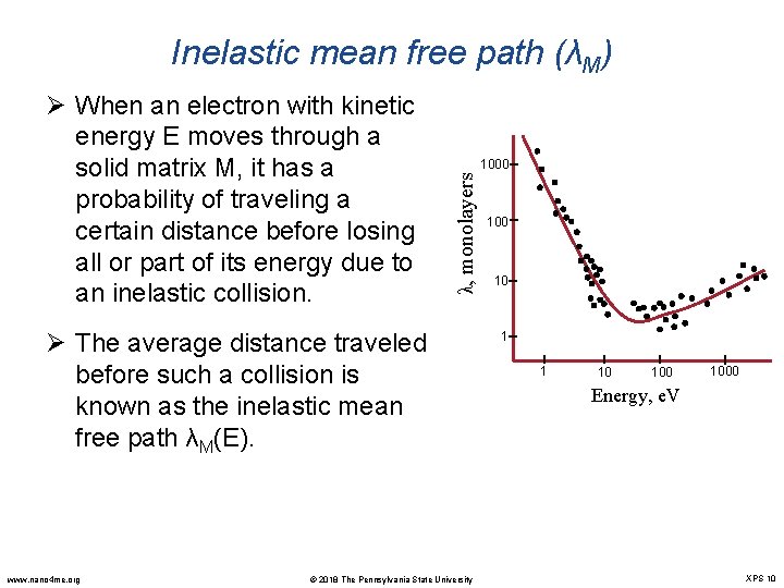
Inelastic mean free path (λM) 1000 λ, monolayers Ø When an electron with kinetic energy E moves through a solid matrix M, it has a probability of traveling a certain distance before losing all or part of its energy due to an inelastic collision. Ø The average distance traveled before such a collision is known as the inelastic mean free path λM(E). www. nano 4 me. org © 2018 The Pennsylvania State University 100 10 1 1 10 1000 Energy, e. V XPS 10

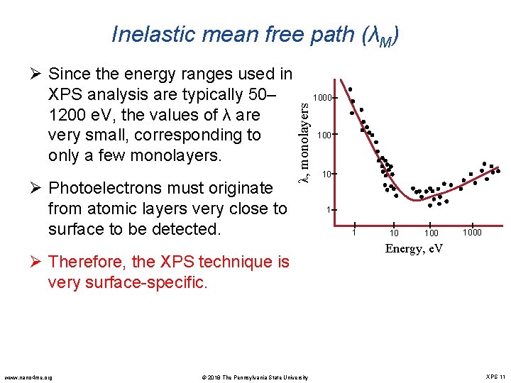
Inelastic mean free path (λM) Ø Photoelectrons must originate from atomic layers very close to surface to be detected. λ, monolayers Ø Since the energy ranges used in XPS analysis are typically 50– 1200 e. V, the values of λ are very small, corresponding to only a few monolayers. Ø Therefore, the XPS technique is very surface-specific. www. nano 4 me. org © 2018 The Pennsylvania State University 1000 10 1 1 10 1000 Energy, e. V XPS 11

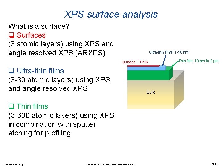
XPS surface analysis What is a surface? q Surfaces (3 atomic layers) using XPS and angle resolved XPS (ARXPS) Ultra-thin films: 1 -10 nm Surface: ~1 nm q Ultra-thin films (3 -30 atomic layers) using XPS and angle resolved XPS Thin film: 10 nm to 2 µm Bulk q Thin films (3 -600 atomic layers) using XPS in combination with sputter etching for profiling www. nano 4 me. org © 2018 The Pennsylvania State University XPS 12

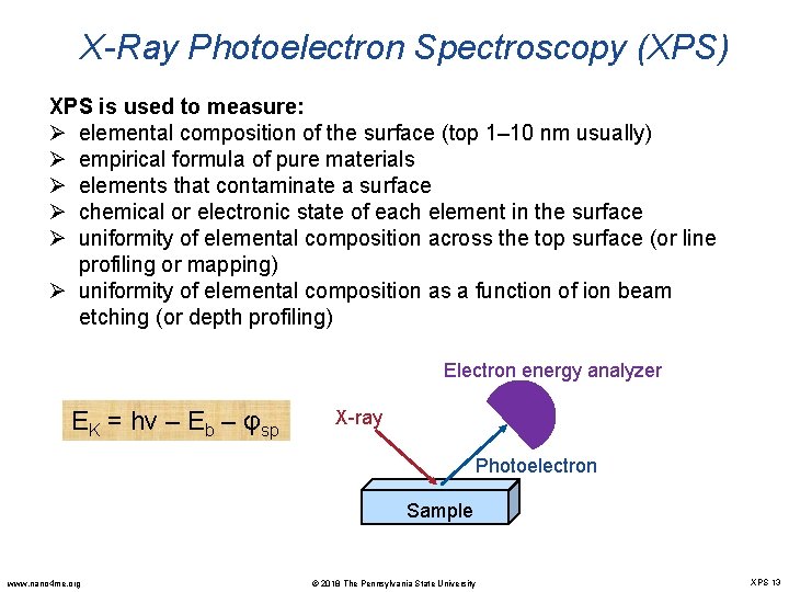
X-Ray Photoelectron Spectroscopy (XPS) XPS is used to measure: Ø elemental composition of the surface (top 1– 10 nm usually) Ø empirical formula of pure materials Ø elements that contaminate a surface Ø chemical or electronic state of each element in the surface Ø uniformity of elemental composition across the top surface (or line profiling or mapping) Ø uniformity of elemental composition as a function of ion beam etching (or depth profiling) Electron energy analyzer EK = hν – Eb – φsp X-ray Photoelectron Sample www. nano 4 me. org © 2018 The Pennsylvania State University XPS 13

Outline Ø Basic principles Ø Instrumentation Ø Peak characteristics Ø Quantitative analysis Ø Depth profiling www. nano 4 me. org © 2018 The Pennsylvania State University XPS 14

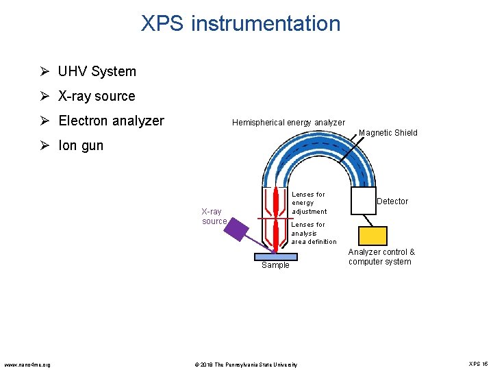
XPS instrumentation Ø UHV System Ø X-ray source Ø Electron analyzer Hemispherical energy analyzer Magnetic Shield Ø Ion gun Lenses for energy adjustment X-ray source Lenses for analysis area definition Sample www. nano 4 me. org Detector © 2018 The Pennsylvania State University Analyzer control & computer system XPS 15

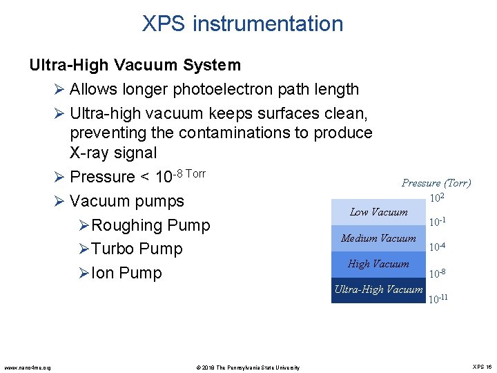
XPS instrumentation Ultra-High Vacuum System Ø Allows longer photoelectron path length Ø Ultra-high vacuum keeps surfaces clean, preventing the contaminations to produce X-ray signal Ø Pressure < 10 -8 Torr Pressure (Torr) 102 Ø Vacuum pumps Low Vacuum 10 -1 ØRoughing Pump Medium Vacuum 10 -4 ØTurbo Pump High Vacuum 10 -8 ØIon Pump Ultra-High Vacuum www. nano 4 me. org © 2018 The Pennsylvania State University 10 -11 XPS 16

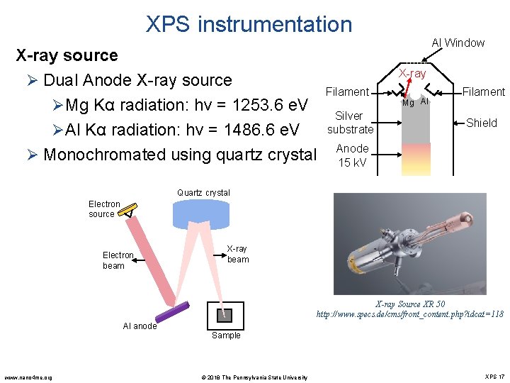
XPS instrumentation X-ray source Ø Dual Anode X-ray source Filament ØMg Kα radiation: hν = 1253. 6 e. V Silver substrate ØAl Kα radiation: hν = 1486. 6 e. V Ø Monochromated using quartz crystal Anode 15 k. V Al Window X-ray Mg Al Filament Shield Quartz crystal Electron source Electron beam X-ray Source XR 50 http: //www. specs. de/cms/front_content. php? idcat=118 Al anode www. nano 4 me. org Sample © 2018 The Pennsylvania State University XPS 17

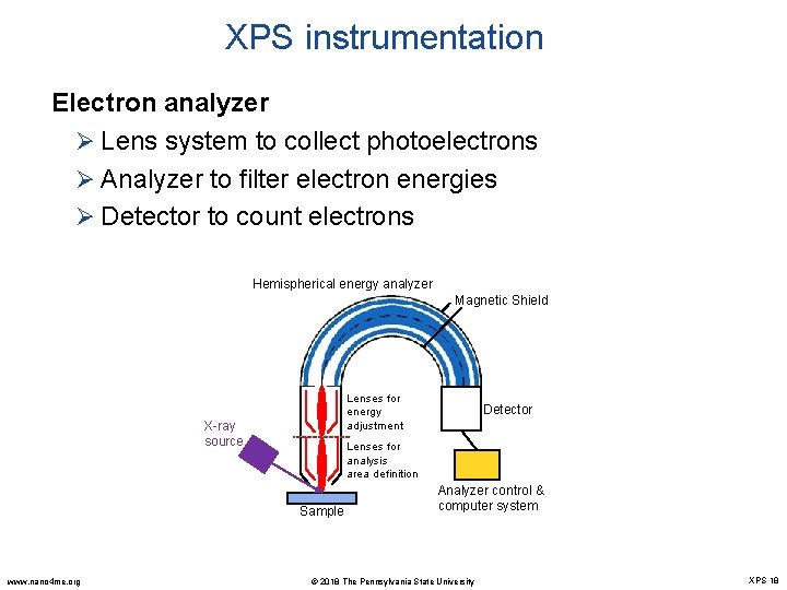
XPS instrumentation Electron analyzer Ø Lens system to collect photoelectrons Ø Analyzer to filter electron energies Ø Detector to count electrons Hemispherical energy analyzer Magnetic Shield Lenses for energy adjustment X-ray source Lenses for analysis area definition Sample www. nano 4 me. org Detector Analyzer control & computer system © 2018 The Pennsylvania State University XPS 18

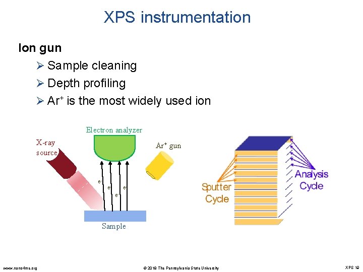
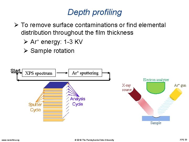
XPS instrumentation Ion gun Ø Sample cleaning Ø Depth profiling Ø Ar+ is the most widely used ion Electron analyzer X-ray source Ar+ gun e- e- ee- Sample www. nano 4 me. org © 2018 The Pennsylvania State University XPS 19

Outline Ø Basic principles Ø Instrumentation Ø Peak characteristics Ø Quantitative analysis Ø Depth profiling www. nano 4 me. org © 2018 The Pennsylvania State University XPS 20

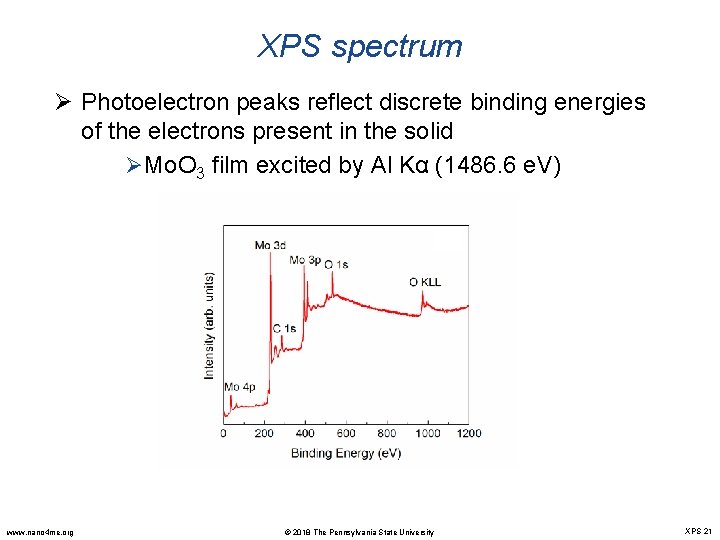
XPS spectrum Ø Photoelectron peaks reflect discrete binding energies of the electrons present in the solid ØMo. O 3 film excited by Al Kα (1486. 6 e. V) www. nano 4 me. org © 2018 The Pennsylvania State University XPS 21

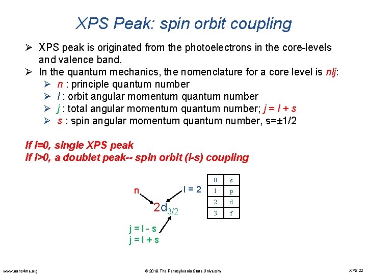
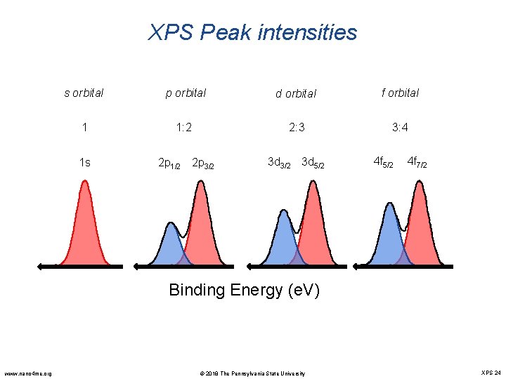
XPS Peak: spin orbit coupling Ø XPS peak is originated from the photoelectrons in the core-levels and valence band. Ø In the quantum mechanics, the nomenclature for a core level is nlj: Ø n : principle quantum number Ø l : orbit angular momentum quantum number Ø j : total angular momentum quantum number; j = l + s Ø s : spin angular momentum quantum number, s=± 1/2 If l=0, single XPS peak if l>0, a doublet peak-- spin orbit (l-s) coupling l = 2 n 2 d 3/2 0 s 1 p 2 d 3 f j = l - s j = l + s www. nano 4 me. org © 2018 The Pennsylvania State University XPS 22

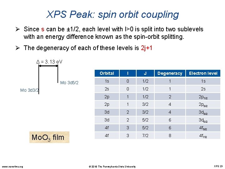
XPS Peak: spin orbit coupling Ø Since s can be ± 1/2, each level with l>0 is split into two sublevels with an energy difference known as the spin-orbit splitting. Ø The degeneracy of each of these levels is 2 j+1 Δ = 3. 13 e. V Mo 3 d 5/2 Mo 3 d 3/2 Mo. O 3 film www. nano 4 me. org Orbital l J Degeneracy Electron level 1 s 0 1/2 1 1 s 2 s 0 1/2 1 2 s 2 p 1 1/2 2 2 p 1/2 2 p 1 3/2 4 2 p 3/2 3 d 2 3/2 4 3 d 3/2 3 d 2 5/2 6 3 d 5/2 4 f 3 5/2 6 4 f 5/2 4 f 3 7/2 8 4 f 7/2 © 2018 The Pennsylvania State University XPS 23

XPS Peak intensities s orbital p orbital d orbital f orbital 1 1: 2 2: 3 3: 4 1 s 2 p 1/2 2 p 3/2 3 d 5/2 4 f 7/2 Binding Energy (e. V) www. nano 4 me. org © 2018 The Pennsylvania State University XPS 24

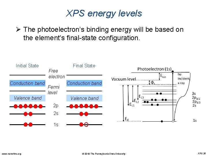
XPS energy levels Ø The photoelectron’s binding energy will be based on the element’s final-state configuration. Initial State Final State Free electron Conduction band Fermi level Valence band Conduction band Valence band 2 p 2 s 1 s www. nano 4 me. org © 2018 The Pennsylvania State University XPS 25

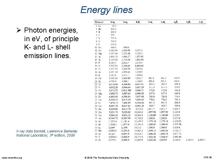
Energy lines Ø Photon energies, in e. V, of principle K- and L- shell emission lines. X-ray data booklet, Lawrence Berkeley National Laboratory, 3 rd edition, 2009 www. nano 4 me. org © 2018 The Pennsylvania State University XPS 26

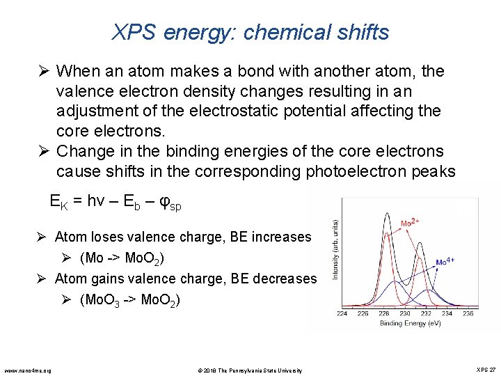
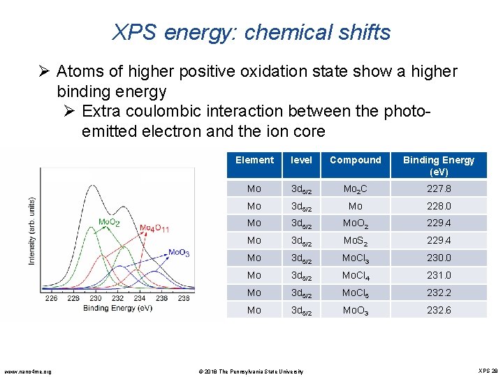
XPS energy: chemical shifts Ø When an atom makes a bond with another atom, the valence electron density changes resulting in an adjustment of the electrostatic potential affecting the core electrons. Ø Change in the binding energies of the core electrons cause shifts in the corresponding photoelectron peaks EK = hν – Eb – φsp Ø Atom loses valence charge, BE increases Ø (Mo -> Mo. O 2) Ø Atom gains valence charge, BE decreases Ø (Mo. O 3 -> Mo. O 2) www. nano 4 me. org © 2018 The Pennsylvania State University XPS 27

XPS energy: chemical shifts Ø Atoms of higher positive oxidation state show a higher binding energy Ø Extra coulombic interaction between the photoemitted electron and the ion core www. nano 4 me. org Element level Compound Binding Energy (e. V) Mo 3 d 5/2 Mo 2 C 227. 8 Mo 3 d 5/2 Mo 228. 0 Mo 3 d 5/2 Mo. O 2 229. 4 Mo 3 d 5/2 Mo. S 2 229. 4 Mo 3 d 5/2 Mo. Cl 3 230. 0 Mo 3 d 5/2 Mo. Cl 4 231. 0 Mo 3 d 5/2 Mo. Cl 5 232. 2 Mo 3 d 5/2 Mo. O 3 232. 6 © 2018 The Pennsylvania State University XPS 28

Outline Ø Basic principles Ø Instrumentation Ø Peak characteristics Ø Quantitative analysis Ø Depth profiling www. nano 4 me. org © 2018 The Pennsylvania State University XPS 29

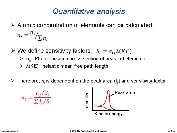
Quantitative analysis Ø Atomic concentration of elements can be calculated: Ø We define sensitivity factors: Ø σij : Photoionization cross-section of peak j of element i Ø λ(KE): Inelastic mean free path length Ø Therefore, ni is dependent on the peak area (Iij) and sensitivity factor Peak area Intensity Kinetic energy www. nano 4 me. org © 2018 The Pennsylvania State University XPS 30

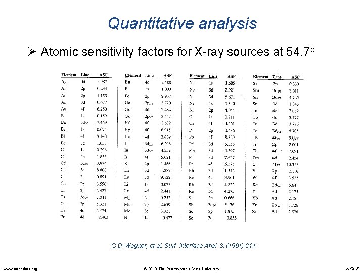
Quantitative analysis Ø Atomic sensitivity factors for X-ray sources at 54. 7 o C. D. Wagner, et al, Surf. Interface Anal. 3, (1981) 211. www. nano 4 me. org © 2018 The Pennsylvania State University XPS 31

Outline Ø Basic principles Ø Instrumentation Ø Peak characteristics Ø Quantitative analysis Ø Depth profiling www. nano 4 me. org © 2018 The Pennsylvania State University XPS 32

Depth profiling Ø To remove surface contaminations or find elemental distribution throughout the film thickness Ø Ar+ energy: 1 -3 KV Ø Sample rotation Start XPS spectrum Ar+ sputtering Electron analyzer X-ray source Ar+ gun Sample www. nano 4 me. org © 2018 The Pennsylvania State University XPS 33

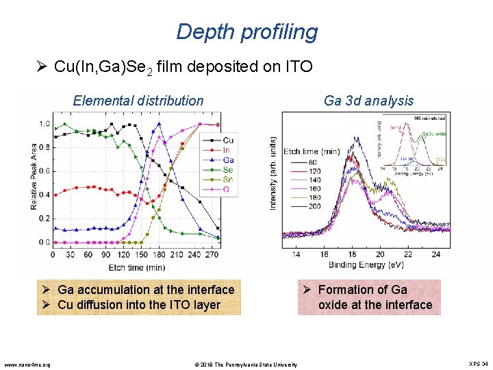
Depth profiling Ø Cu(In, Ga)Se 2 film deposited on ITO Elemental distribution Ga 3 d analysis Ø Ga accumulation at the interface Ø Cu diffusion into the ITO layer Ø Formation of Ga oxide at the interface www. nano 4 me. org © 2018 The Pennsylvania State University XPS 34

Summary Vacuum Range Ø Requires ultra high vacuum Ø Sample compatibility with UHV environment may be an issue with biological samples Sensitivity Ø Measures the elemental composition of the top 10 nm Ø Can detect all elements except H and He Ø Detection limits typically ~ 0. 1 atomic percent Ø Typically the smallest analytical area ~10 µm Material analysis Ø Can analyze metals, inorganic, polymers Ø Sample compatibility with UHV environment www. nano 4 me. org © 2018 The Pennsylvania State University XPS 35

Online sources • PNNL EMSL: www. emsl. gov • AVS Science & Technology Society: www. avs. org • AVS Surface Science Spectra: www. avs. org/literature. sss. aspx • Evans Analytical Group: www. cea. com • NIST X-ray Photoelectron Spectroscopy Database: www. srdata. nist. gov/sps/ • NIST Electron Inelastic-Mean-Free-Path Database: www. nist. gov/srd/nist 71. htm • QUASES-IMFP-TPP 2 M QUASES-Tougaard Inc. : www. quases. com • Surfaces & Interfaces Section, National Physical Lab. www. npl. co. uk/npl/cmmt/sis • XPS Multi. Quant www. chemres. hu/aki/XMQpages/XMQhome. htm • ASTM International: www. astm. org www. nano 4 me. org © 2018 The Pennsylvania State University XPS 36