XPS X ray photoemission spectroscopy ESCA Electron Spectroscopy
- Slides: 46

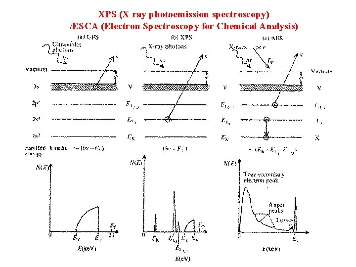
XPS (X ray photoemission spectroscopy) /ESCA (Electron Spectroscopy for Chemical Analysis)

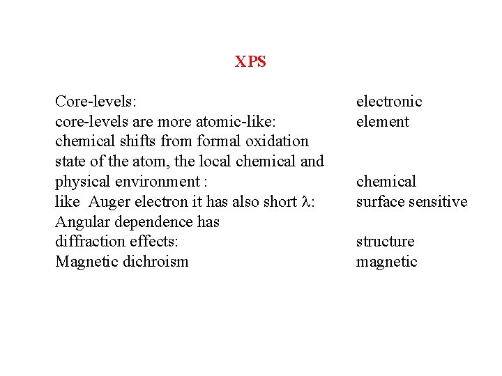
XPS Core-levels: core-levels are more atomic-like: chemical shifts from formal oxidation state of the atom, the local chemical and physical environment : like Auger electron it has also short l: Angular dependence has diffraction effects: Magnetic dichroism electronic element chemical surface sensitive structure magnetic

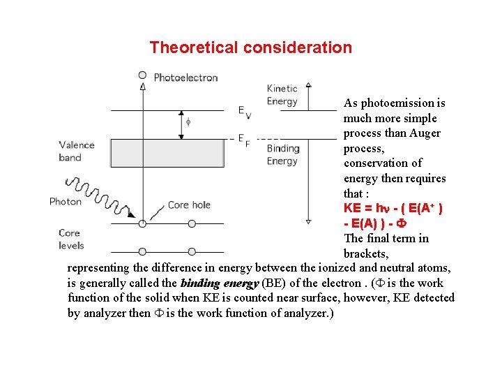
Theoretical consideration As photoemission is much more simple process than Auger process, conservation of energy then requires that : KE = hn - ( E(A+ ) - E(A) ) - F The final term in brackets, representing the difference in energy between the ionized and neutral atoms, is generally called the binding energy (BE) of the electron. (F is the work function of the solid when KE is counted near surface, however, KE detected by analyzer then F is the work function of analyzer. )

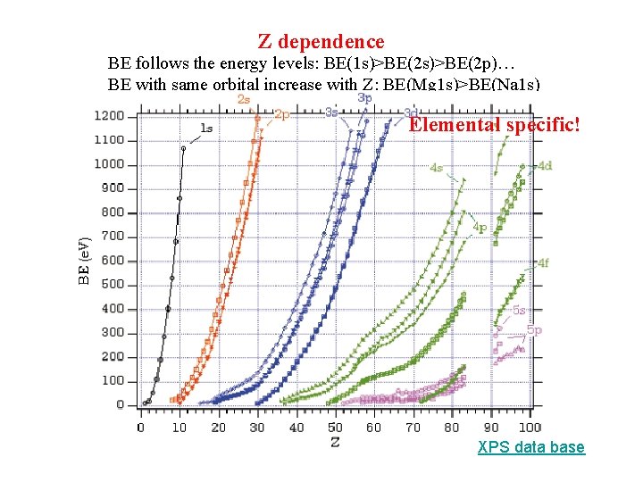
Z dependence BE follows the energy levels: BE(1 s)>BE(2 p)… BE with same orbital increase with Z: BE(Mg 1 s)>BE(Na 1 s) Elemental specific! XPS data base

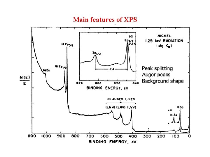
Main features of XPS

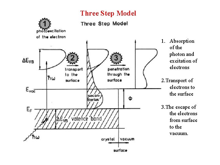
Three Step Model 1. Absorption of the photon and excitation of electrons 2. Transport of electrons to the surface 3. The escape of the electrons from surface to the vacuum.

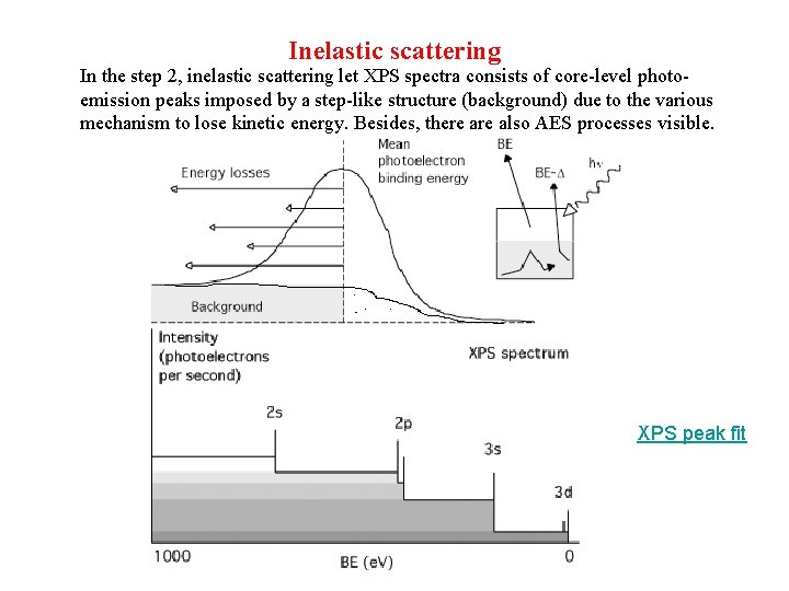
Inelastic scattering In the step 2, inelastic scattering let XPS spectra consists of core-level photoemission peaks imposed by a step-like structure (background) due to the various mechanism to lose kinetic energy. Besides, there also AES processes visible. XPS peak fit

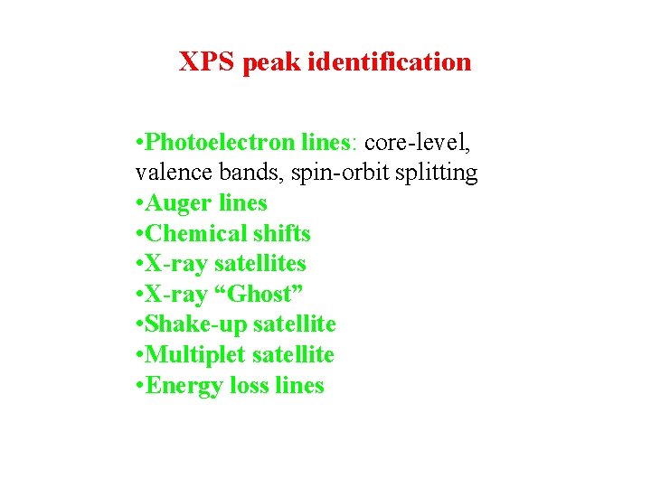
XPS peak identification • Photoelectron lines: core-level, valence bands, spin-orbit splitting • Auger lines • Chemical shifts • X-ray satellites • X-ray “Ghost” • Shake-up satellite • Multiplet satellite • Energy loss lines

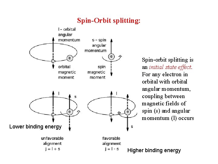
Spin-Orbit splitting: Spin-orbit splitting is an initial state effect. For any electron in orbital with orbital angular momentum, coupling between magnetic fields of spin (s) and angular momentum (l) occurs Lower binding energy Higher binding energy

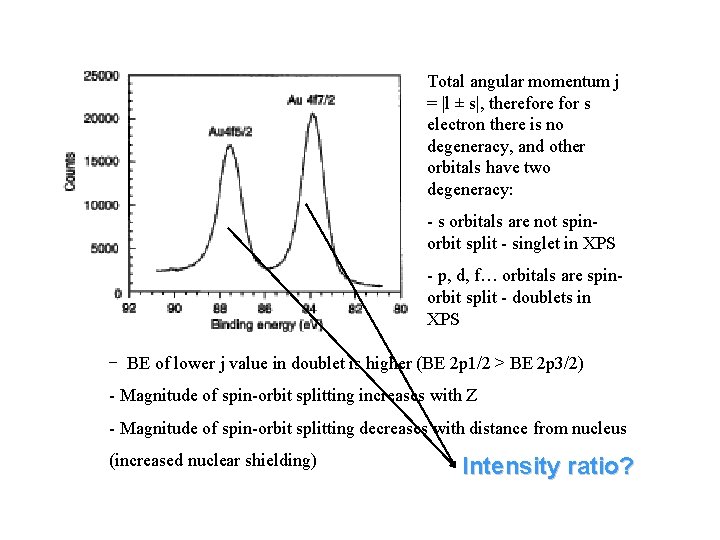
Total angular momentum j = |l ± s|, therefore for s electron there is no degeneracy, and other orbitals have two degeneracy: - s orbitals are not spinorbit split - singlet in XPS - p, d, f… orbitals are spinorbit split - doublets in XPS - BE of lower j value in doublet is higher (BE 2 p 1/2 > BE 2 p 3/2) - Magnitude of spin-orbit splitting increases with Z - Magnitude of spin-orbit splitting decreases with distance from nucleus (increased nuclear shielding) Intensity ratio?

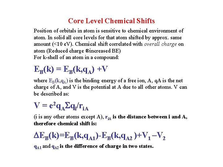
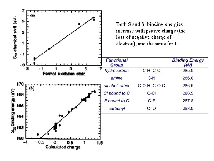
Core Level Chemical Shifts Position of orbitals in atom is sensitive to chemical environment of atom. In solid all core levels for that atom shifted by approx. same amount (<10 e. V). Chemical shift correlated with overall charge on atom (Reduced charge ®increased BE) For k-shell of an atom in a compound: EB(k) = EB(k, q. A) +V where EB(k, q. A) is the binding energy of a free ion, A, q. A is the net charge of A, and V is the potential at A due to all other atoms. V can be described as: V = e 2 q. ASqi/ri. A (i is any other atoms except A), ri. A is the distance between i and A, therefore chemical shift is: DEB(k)=EB(k, q. A 1)-EB(k, q. A 2 )+V 1 –V 2 q. A 1 and q. A 2 is the difference of charge in two states.

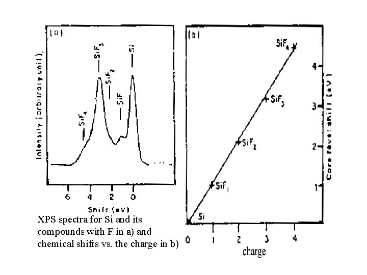
XPS spectra for Si and its compounds with F in a) and chemical shifts vs. the charge in b)

Both S and Si binding energies increase with psitive charge (the loss of negative charge of electron), and the same for C.

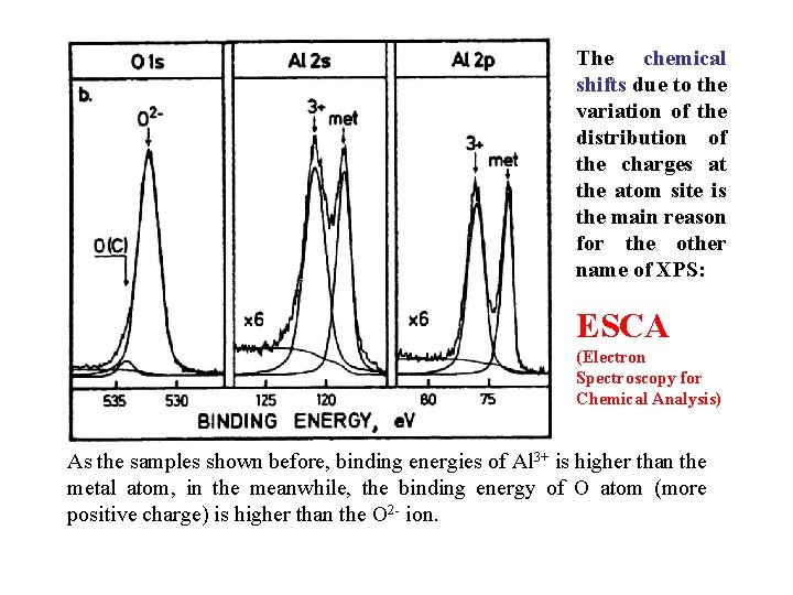
The chemical shifts due to the variation of the distribution of the charges at the atom site is the main reason for the other name of XPS: ESCA (Electron Spectroscopy for Chemical Analysis) As the samples shown before, binding energies of Al 3+ is higher than the metal atom, in the meanwhile, the binding energy of O atom (more positive charge) is higher than the O 2 - ion.

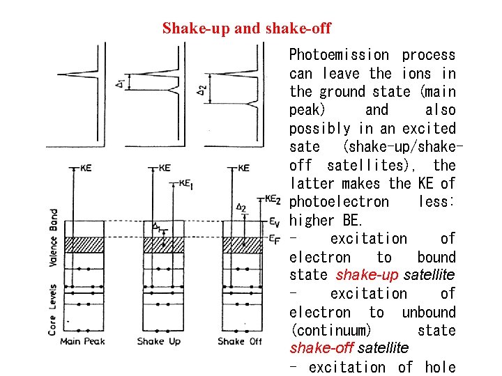
Shake-up and shake-off Photoemission process can leave the ions in the ground state (main peak) and also possibly in an excited sate (shake-up/shakeoff satellites), the latter makes the KE of photoelectron less: higher BE. excitation of electron to bound state shake-up satellite excitation of electron to unbound (continuum) state shake-off satellite - excitation of hole

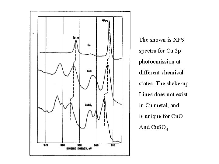
The shown is XPS spectra for Cu 2 p photoemission at different chemical states. The shake-up Lines does not exist in Cu metal, and is unique for Cu. O And Cu. SO 4

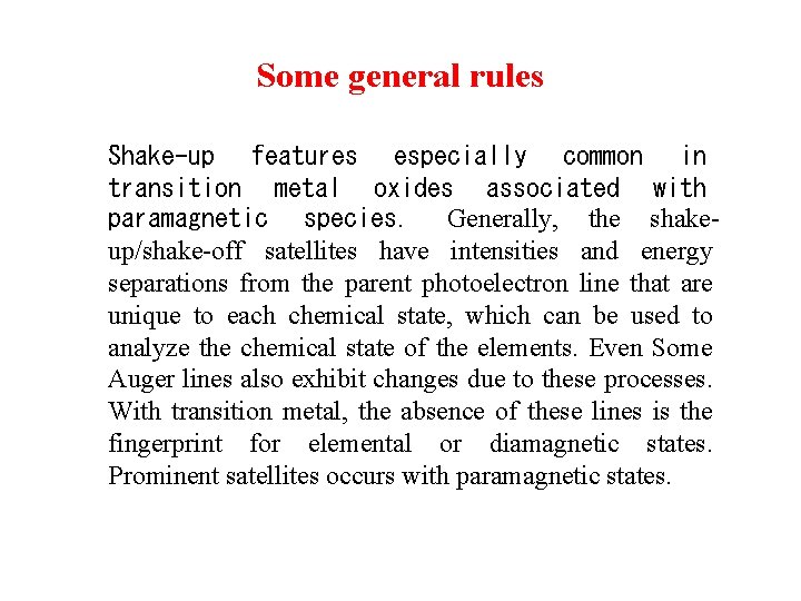
Some general rules Shake-up features especially common in transition metal oxides associated with paramagnetic species. Generally, the shakeup/shake-off satellites have intensities and energy separations from the parent photoelectron line that are unique to each chemical state, which can be used to analyze the chemical state of the elements. Even Some Auger lines also exhibit changes due to these processes. With transition metal, the absence of these lines is the fingerprint for elemental or diamagnetic states. Prominent satellites occurs with paramagnetic states.

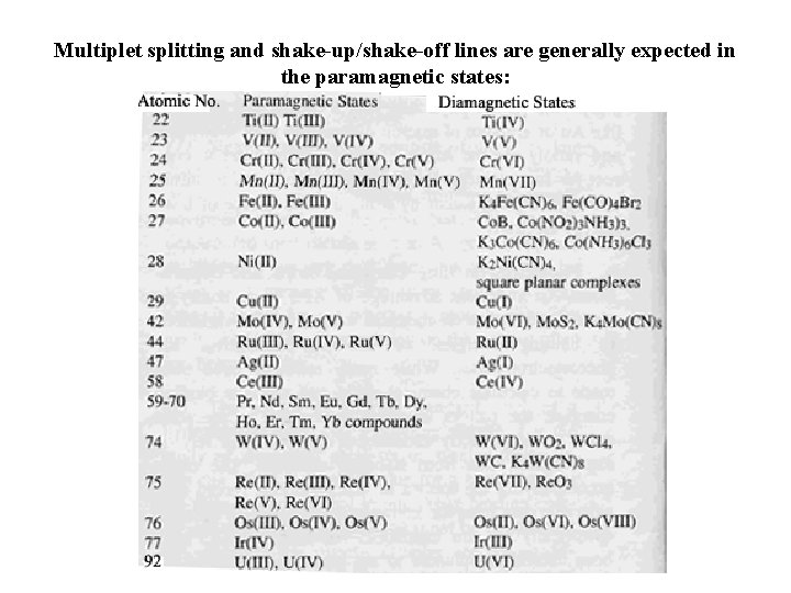
Multiplet splitting and shake-up/shake-off lines are generally expected in the paramagnetic states:

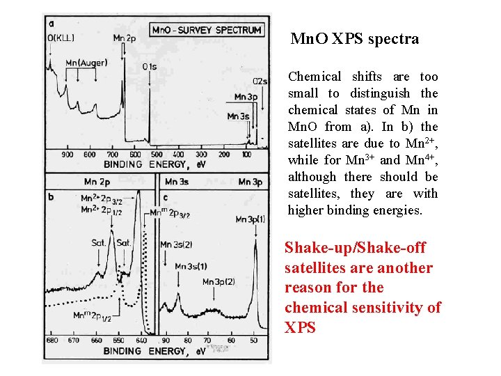
Mn. O XPS spectra Chemical shifts are too small to distinguish the chemical states of Mn in Mn. O from a). In b) the satellites are due to Mn 2+, while for Mn 3+ and Mn 4+, although there should be satellites, they are with higher binding energies. Shake-up/Shake-off satellites are another reason for the chemical sensitivity of XPS

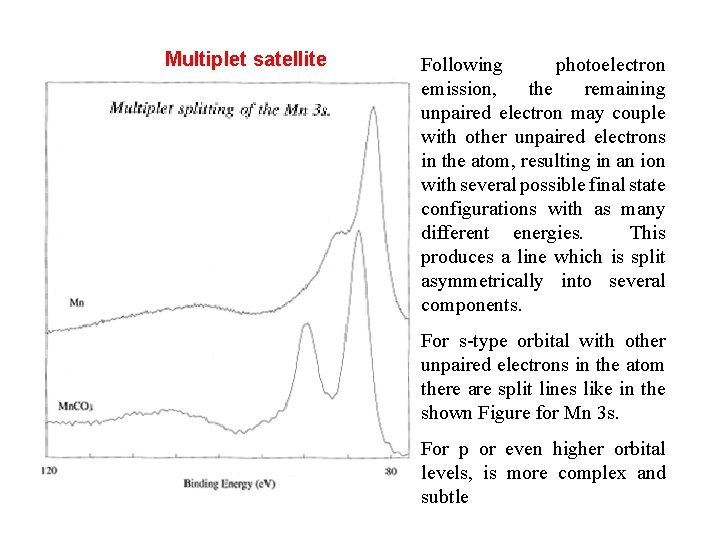
Multiplet satellite Following photoelectron emission, the remaining unpaired electron may couple with other unpaired electrons in the atom, resulting in an ion with several possible final state configurations with as many different energies. This produces a line which is split asymmetrically into several components. For s-type orbital with other unpaired electrons in the atom there are split lines like in the shown Figure for Mn 3 s. For p or even higher orbital levels, is more complex and subtle

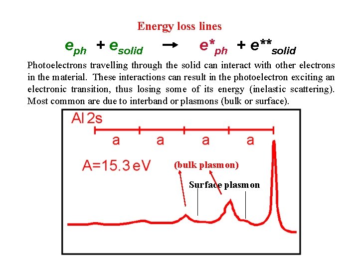
Energy loss lines eph + esolid e*ph + e**solid Photoelectrons travelling through the solid can interact with other electrons in the material. These interactions can result in the photoelectron exciting an electronic transition, thus losing some of its energy (inelastic scattering). Most common are due to interband or plasmons (bulk or surface). (bulk plasmon) Surface plasmon

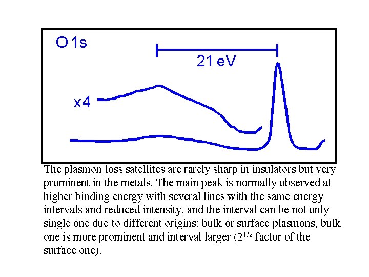
The plasmon loss satellites are rarely sharp in insulators but very prominent in the metals. The main peak is normally observed at higher binding energy with several lines with the same energy intervals and reduced intensity, and the interval can be not only single one due to different origins: bulk or surface plasmons, bulk one is more prominent and interval larger (21/2 factor of the surface one).

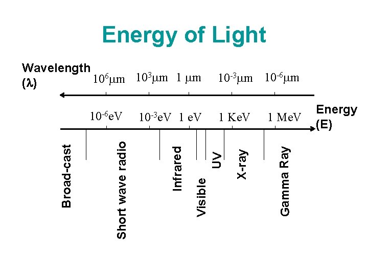
Energy of Light 1 Me. V Gamma Ray 1 Ke. V UV 1 e. V Visible 10 -3 e. V Infrared Short wave radio Broad-cast 10 -6 e. V 10 -3 m 10 -6 m X-ray Wavelength 6 m 103 m 10 ( ) Energy (E)

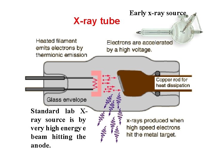
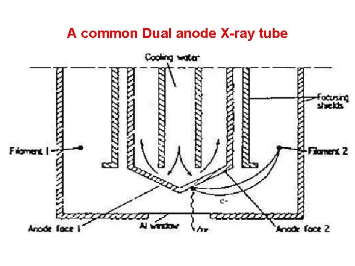
X-ray tube Standard lab Xray source is by very high energy e beam hitting the anode. Early x-ray source

A common Dual anode X-ray tube

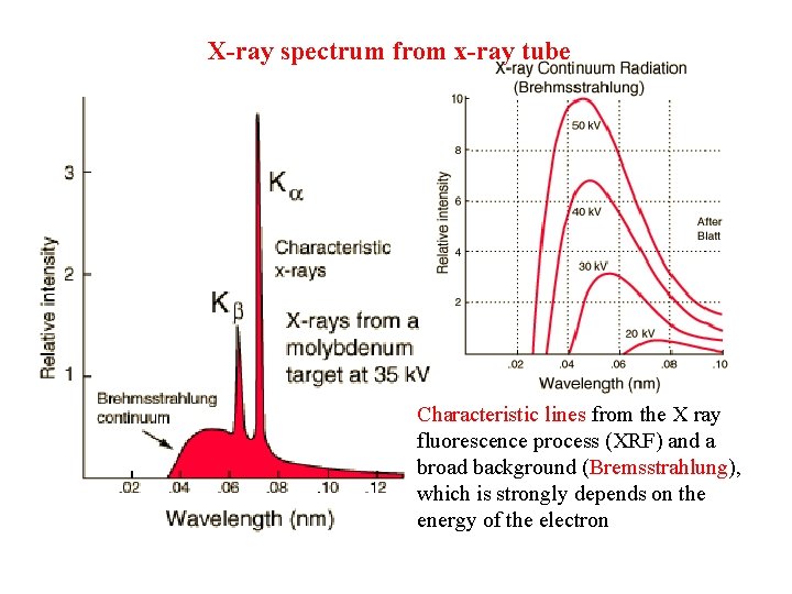
X-ray spectrum from x-ray tube Characteristic lines from the X ray fluorescence process (XRF) and a broad background (Bremsstrahlung), which is strongly depends on the energy of the electron

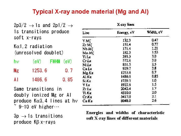
Typical X-ray anode material (Mg and Al) 2 p 3/2 ® 1 s and 2 p 1/2 ® 1 s transitions produce soft x-rays Ka 1, 2 radiation (unresolved doublet) hn (e. V) FWHM (e. V) Mg 1253. 6 0. 7 Al 1486. 6 0. 85 Same transitions in doubly ionized Mg or Al produce Ka 3, 4 lines at hn ~ 9 -10 e. V higher… 3 p ® 1 s transitions produce Kb x-rays Energies and widths of characteristic soft X-ray lines of different materials

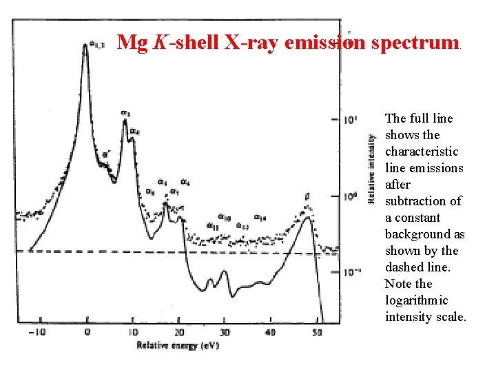
Mg K-shell X-ray emission spectrum . The full line shows the characteristic line emissions after subtraction of a constant background as shown by the dashed line. Note the logarithmic intensity scale.

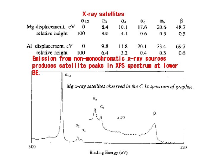
X-ray satellites Emission from non-monochromatic x-ray sources produces satellite peaks in XPS spectrum at lower BE.

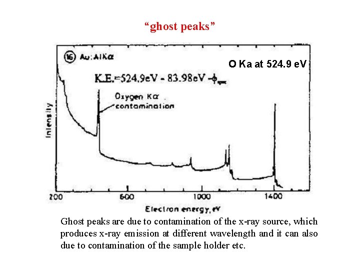
“ghost peaks” O Ka at 524. 9 e. V Ghost peaks are due to contamination of the x-ray source, which produces x-ray emission at different wavelength and it can also due to contamination of the sample holder etc.

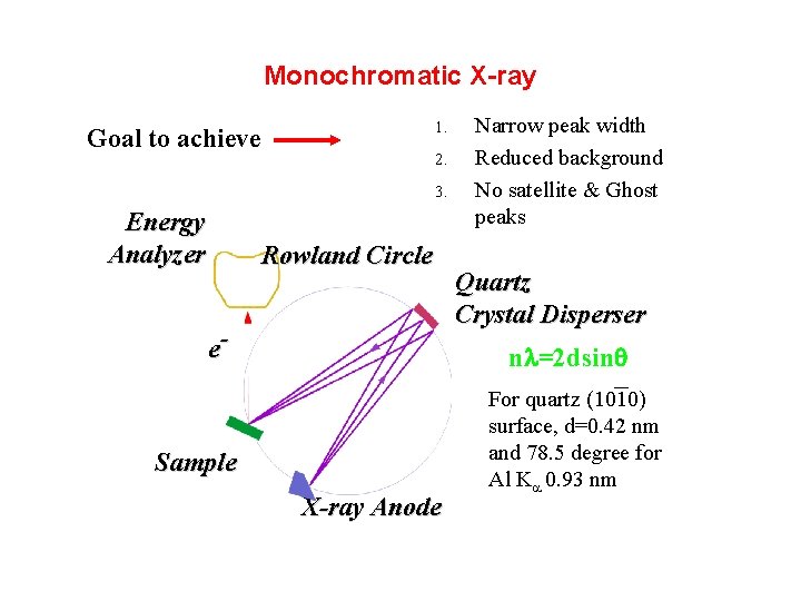
Monochromatic X-ray 1. Goal to achieve 2. 3. Energy Analyzer Rowland Circle e- Narrow peak width Reduced background No satellite & Ghost peaks Quartz Crystal Disperser n =2 dsinq Sample X-ray Anode For quartz (1010) surface, d=0. 42 nm and 78. 5 degree for Al Ka 0. 93 nm

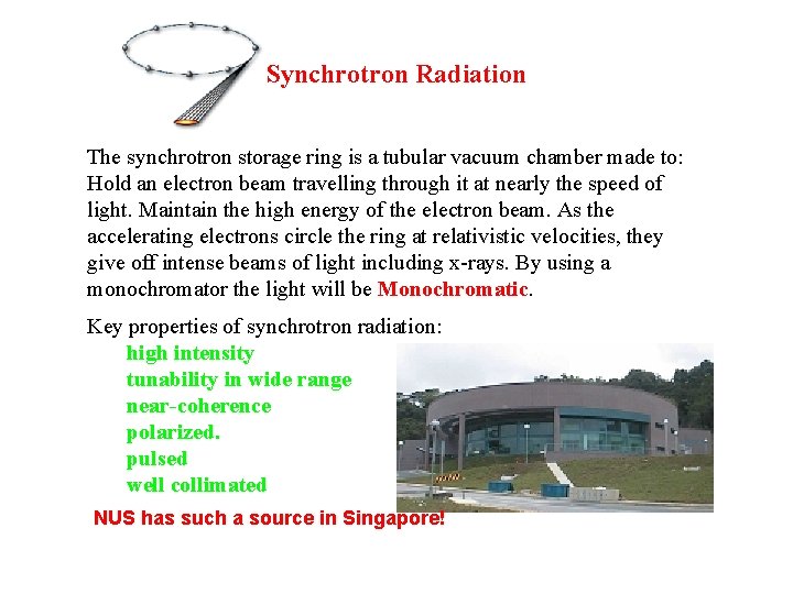
Synchrotron Radiation The synchrotron storage ring is a tubular vacuum chamber made to: Hold an electron beam travelling through it at nearly the speed of light. Maintain the high energy of the electron beam. As the accelerating electrons circle the ring at relativistic velocities, they give off intense beams of light including x-rays. By using a monochromator the light will be Monochromatic. Key properties of synchrotron radiation: high intensity tunability in wide range near-coherence polarized. pulsed well collimated NUS has such a source in Singapore!

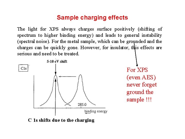
Sample charging effects The light for XPS always charges surface positively (shifting of spectrum to higher binding energy) and leads to general instability (spectral noise). For the metal sample, which can be grounded and the charges can be quickly gone. However, for insulator, this effects are serious and need to be treated. For XPS (even AES) never forget ground the sample !!! C 1 s shifts due to the charging

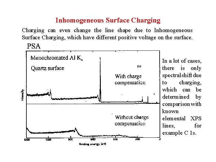
Inhomogeneous Surface Charging can even change the line shape due to Inhomogeneous Surface Charging, which have different positive voltage on the surface. In a lot of cases, there is only spectral shift due to charging, which can be determined by comparison with known elemental XPS lines, for example C 1 s.

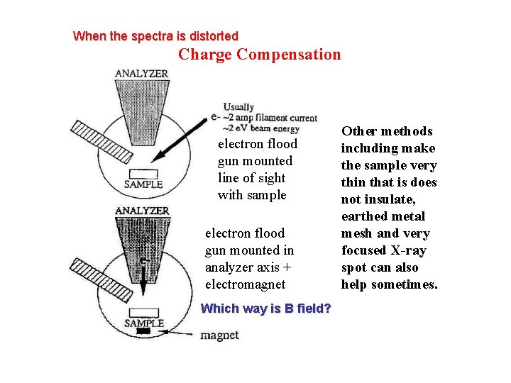
When the spectra is distorted Charge Compensation electron flood gun mounted line of sight with sample electron flood gun mounted in analyzer axis + electromagnet Which way is B field? Other methods including make the sample very thin that is does not insulate, earthed metal mesh and very focused X-ray spot can also help sometimes.

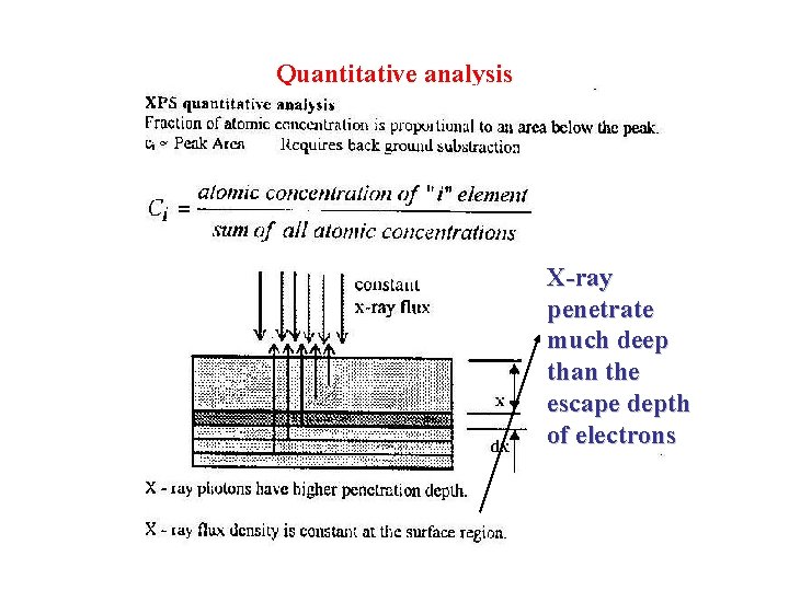
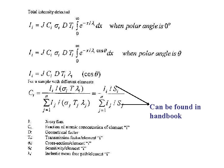
Quantitative analysis X-ray penetrate much deep than the escape depth of electrons

Can be found in handbook

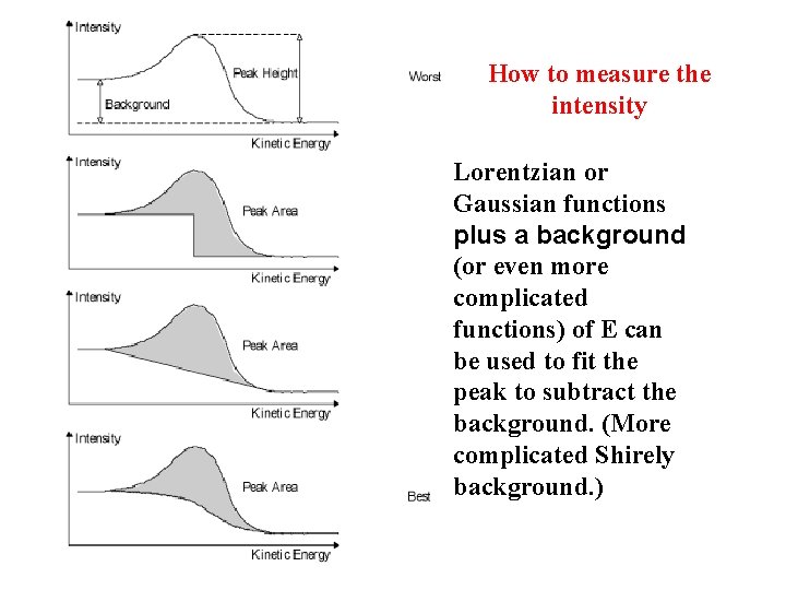
How to measure the intensity Lorentzian or Gaussian functions plus a background (or even more complicated functions) of E can be used to fit the peak to subtract the background. (More complicated Shirely background. )

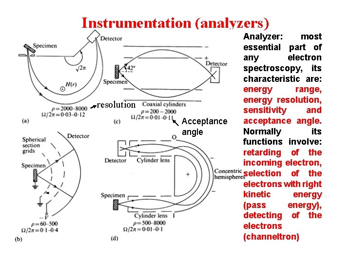
Instrumentation (analyzers) resolution Acceptance angle Analyzer: most essential part of any electron spectroscopy, its characteristic are: energy range, energy resolution, sensitivity and acceptance angle. Normally its functions involve: retarding of the incoming electron, selection of the electrons with right kinetic energy (pass energy), detecting of the electrons (channeltron)

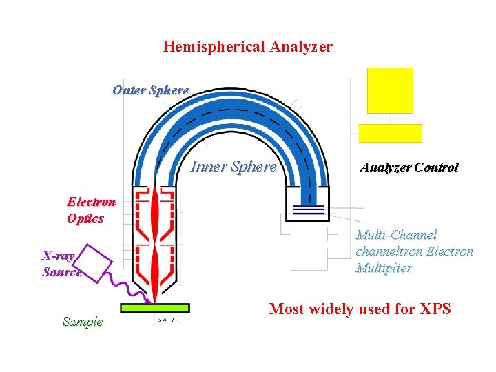
Hemispherical Analyzer Outer Sphere Inner Sphere Analyzer Control Electron Optics X-ray Source Sample Multi-Channel channeltron Electron Multiplier Most widely used for XPS

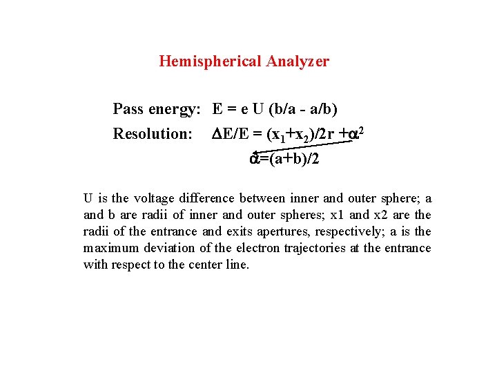
Hemispherical Analyzer Pass energy: E = e U (b/a - a/b) Resolution: DE/E = (x 1+x 2)/2 r +a 2 a=(a+b)/2 U is the voltage difference between inner and outer sphere; a and b are radii of inner and outer spheres; x 1 and x 2 are the radii of the entrance and exits apertures, respectively; a is the maximum deviation of the electron trajectories at the entrance with respect to the center line.

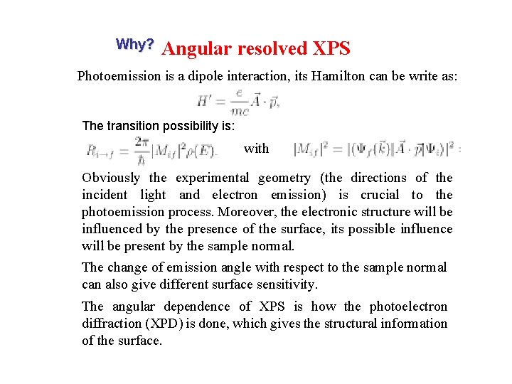
Why? Angular resolved XPS Photoemission is a dipole interaction, its Hamilton can be write as: The transition possibility is: with Obviously the experimental geometry (the directions of the incident light and electron emission) is crucial to the photoemission process. Moreover, the electronic structure will be influenced by the presence of the surface, its possible influence will be present by the sample normal. The change of emission angle with respect to the sample normal can also give different surface sensitivity. The angular dependence of XPS is how the photoelectron diffraction (XPD) is done, which gives the structural information of the surface.

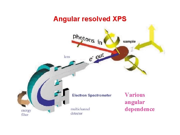
Angular resolved XPS Various angular dependence

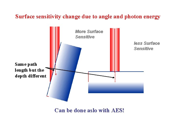
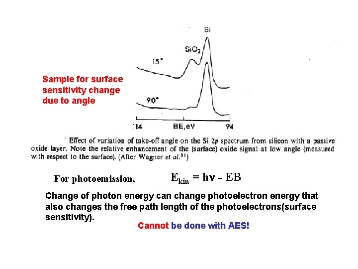
Surface sensitivity change due to angle and photon energy More Surface Sensitive less Surface Sensitive Same path length but the depth different Can be done aslo with AES!

Sample for surface sensitivity change due to angle For photoemission, Ekin = hn - EB Change of photon energy can change photoelectron energy that also changes the free path length of the photoelectrons(surface sensitivity). Cannot be done with AES!

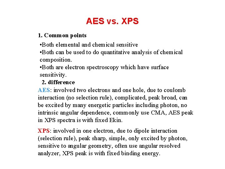
AES vs. XPS 1. Common points • Both elemental and chemical sensitive • Both can be used to do quantitative analysis of chemical composition. • Both are electron spectroscopy which have surface sensitivity. 2. difference AES: involved two electrons and one hole, due to coulomb interaction (no selection rule), complicated, peak broad, can be excited by many energetic particles including photon, no intrinsic angular dependence, commonly use CMA, AES peak in XPS spectra is with fixed Ekin. XPS: involved in one electron, due to dipole interaction (selection rule), peak sharp, simple, only excited by photon, sensitive to angular geometry, often use angular resolved analyzer, XPS peak is with fixed binding energy.