Wireless Laptop Charger Onur Cam Enrique Ramirez Jason


- Slides: 34

Wireless Laptop Charger Onur Cam, Enrique Ramirez, Jason Kao Group 37

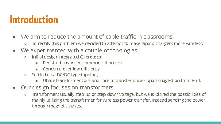
Introduction ● We aim to reduce the amount of cable traffic in classrooms. ○ To rectify this problem we decided to attempt to make laptop chargers more wireless. ● We experimented with a couple of topologies. ○ ○ Initial design integrated Qi protocol. ■ Required advanced communication unit ■ Concerns over low efficiency Settled on a DC/DC type topology. ■ Utilize transformer coils and core to transfer power upon suggestion from Prof. ● Our design focuses on transformers. ○ Transformers usually step-up or step-down voltage, but we explored the possibilities of mainly utilizing the transformer for wireless power transfer, instead sending the power through magnetic waves.

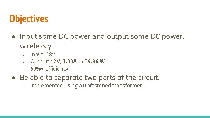
Objectives ● Input some DC power and output some DC power, wirelessly. ○ Input: 18 V ○ Output: 12 V, 3. 33 A → 39. 96 W ○ 60%+ efficiency ● Be able to separate two parts of the circuit. ○ Implemented using a unfastened transformer.

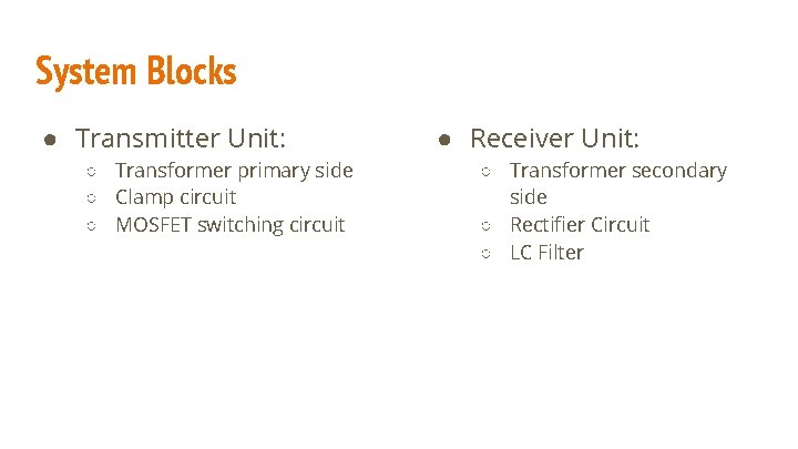
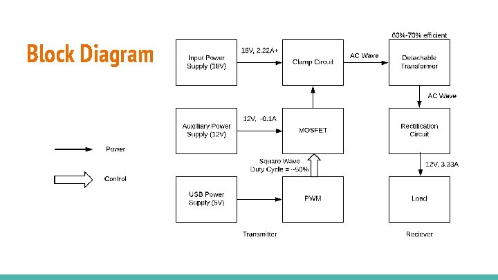
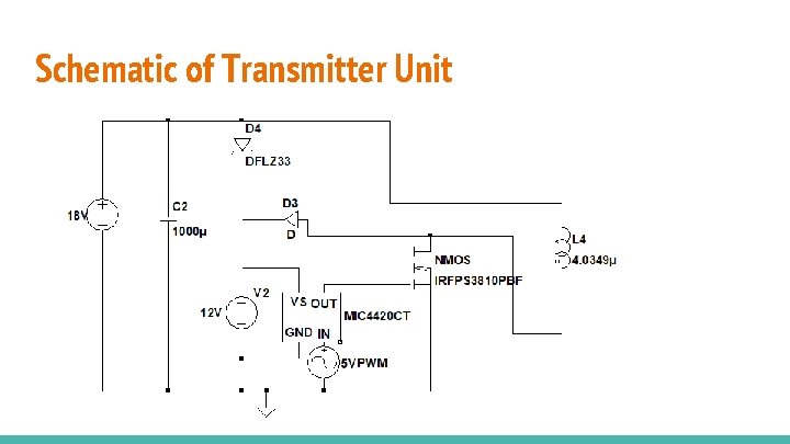
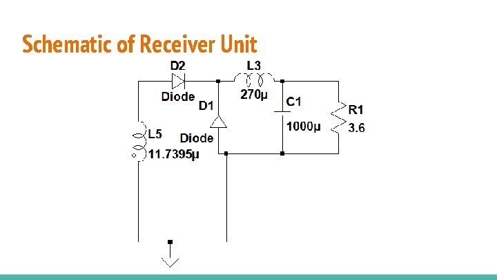
System Blocks ● Transmitter Unit: ○ Transformer primary side ○ Clamp circuit ○ MOSFET switching circuit ● Receiver Unit: ○ Transformer secondary side ○ Rectifier Circuit ○ LC Filter

Block Diagram

Schematic of Transmitter Unit

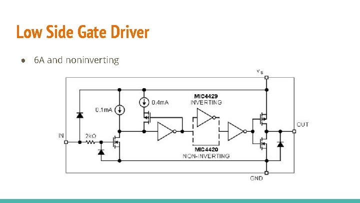
Low Side Gate Driver ● 6 A and noninverting

Schematic of Receiver Unit

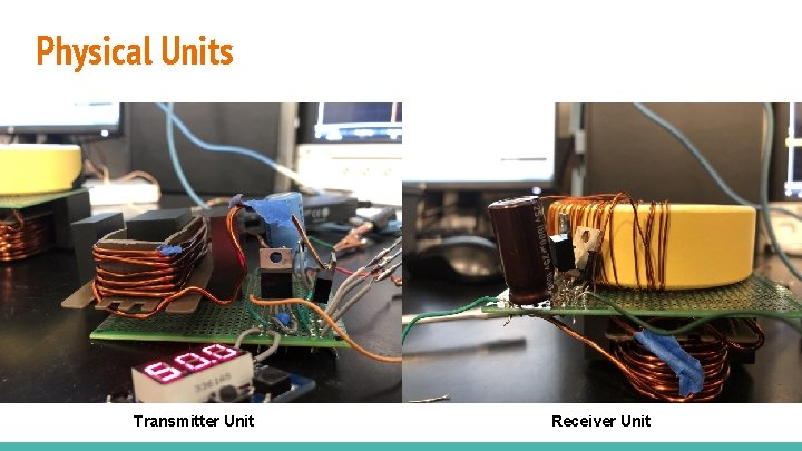
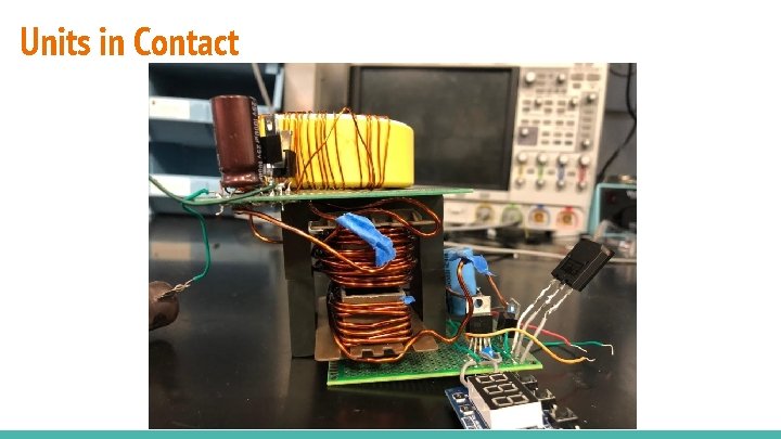
Physical Units Transmitter Unit Receiver Unit

Units in Contact

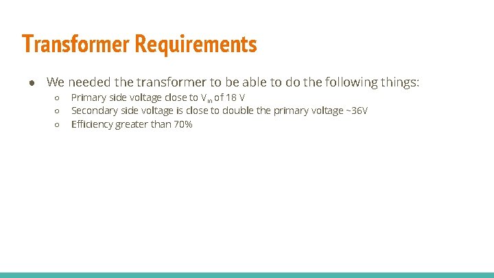
Transformer Requirements ● We needed the transformer to be able to do the following things: ○ ○ ○ Primary side voltage close to Vin of 18 V Secondary side voltage is close to double the primary voltage ~36 V Efficiency greater than 70%

Transformer Core Specifications ● ● A transformer requires a core to amplify and focus magnetic fields ○ We decided on a ferrite core for convenience and high frequency range Effective Magnetic Cross-Section (Ae) ○ ● 535 mm 2 Saturation Magnetization (Bsat) ○ 320 m. T

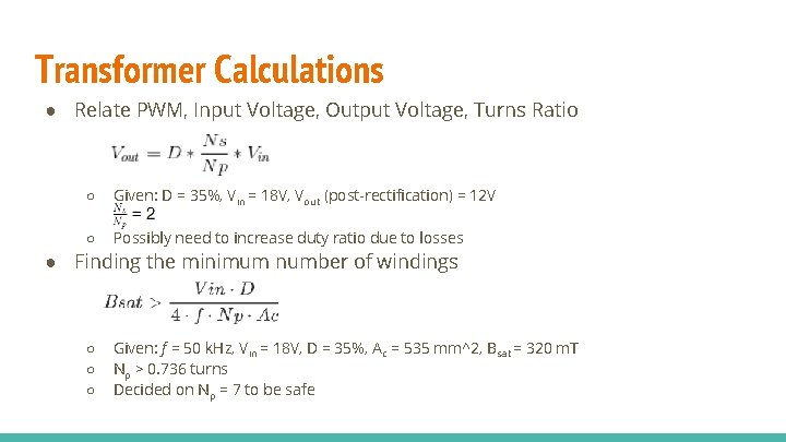
Transformer Calculations ● Relate PWM, Input Voltage, Output Voltage, Turns Ratio ○ Given: D = 35%, Vin = 18 V, Vout (post-rectification) = 12 V ○ Possibly need to increase duty ratio due to losses ● Finding the minimum number of windings ○ ○ ○ Given: f = 50 k. Hz, Vin = 18 V, D = 35%, Ac = 535 mm^2, Bsat = 320 m. T Np > 0. 736 turns Decided on Np = 7 to be safe

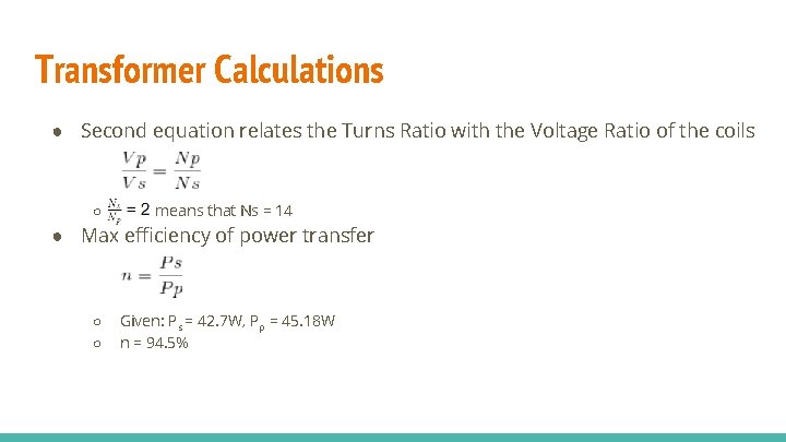
Transformer Calculations ● Second equation relates the Turns Ratio with the Voltage Ratio of the coils ○ means that Ns = 14 ● Max efficiency of power transfer ○ ○ Given: Ps = 42. 7 W, Pp = 45. 18 W n = 94. 5%

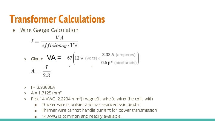
Transformer Calculations ● Wire Gauge Calculation ○ Given: VA = 67 (12 V * 3. 33 A / 0. 6 PF), efficiency = 0. 945, Vp = 18 V ○ ○ ○ I = 3. 93886 A A = 1. 7125 mm 2 Pick 14 AWG (2. 2204 mm 2) magnetic wire to wind the coils with ■ Thicker wire is bulkier and has reduced skin depth ■ Thinner wire cannot handle current for power transmission ■ 14 AWG is common and readily available

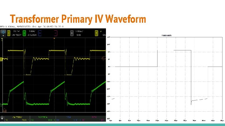
Transformer Primary IV Waveform

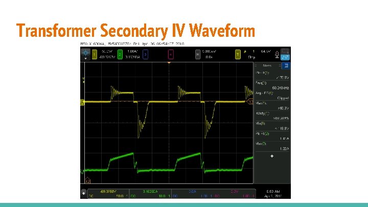
Transformer Secondary IV Waveform

Switching Circuit(Clamp Circuit) Requirements ● Switching Circuit requirements are the following: ○ ○ Reset the Core Vc > 30 V

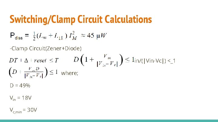
Switching/Clamp Circuit Calculations Pdiss= 1/2 (Lm+L 1 k (Im)^2 =~ 45 u. W -Clamp Circuit(Zener+Diode) DT+Deltareset <_ T D+Vin/|Vin-Vc|<_1 where; D = 49% Vin = 18 V Vc, min = 30 V so P(1+(Vin/(|Vin-Vc|) <_1

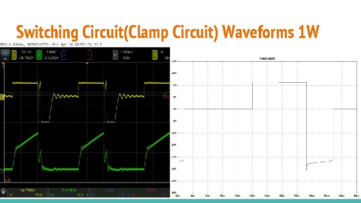
Switching Circuit(Clamp Circuit) Waveforms 1 W

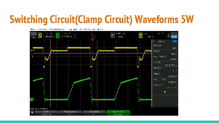
Switching Circuit(Clamp Circuit) Waveforms 5 W

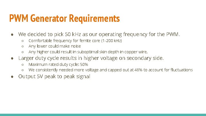
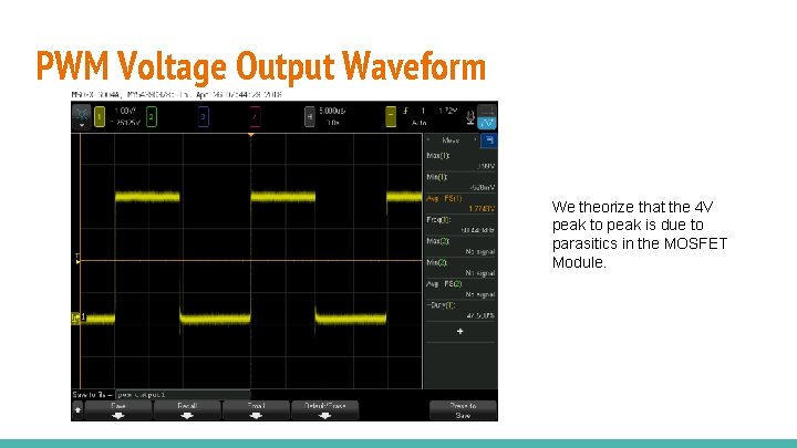
PWM Generator Requirements ● We decided to pick 50 k. Hz as our operating frequency for the PWM. ○ ○ ○ Comfortable frequency for ferrite core (1 -200 k. Hz) Any lower could make noise Any higher could result in suboptimal skin depth in copper wire. ● Larger duty cycle results in higher voltage on secondary side. ○ ○ Maximum rated duty cycle: 50% We consistently needed more voltage and capped out at 48% to account for fluctuations ● Output 5 V peak to peak signal

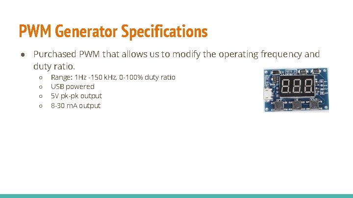
PWM Generator Specifications ● Purchased PWM that allows us to modify the operating frequency and duty ratio. ○ ○ Range: 1 Hz -150 k. Hz, 0 -100% duty ratio USB powered 5 V pk-pk output 8 -30 m. A output

PWM Voltage Output Waveform We theorize that the 4 V peak to peak is due to parasitics in the MOSFET Module.

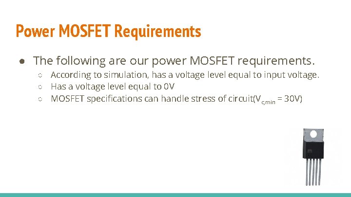
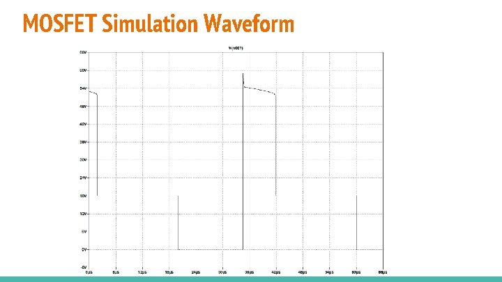
Power MOSFET Requirements ● The following are our power MOSFET requirements. ○ According to simulation, has a voltage level equal to input voltage. ○ Has a voltage level equal to 0 V ○ MOSFET specifications can handle stress of circuit(Vc, min = 30 V)

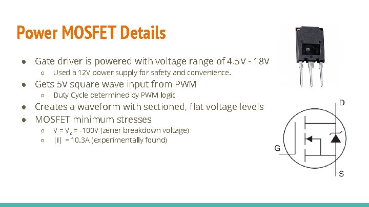
Power MOSFET Details ● Gate driver is powered with voltage range of 4. 5 V - 18 V ○ Used a 12 V power supply for safety and convenience. ● Gets 5 V square wave input from PWM ○ Duty Cycle determined by PWM logic ● Creates a waveform with sectioned, flat voltage levels ● MOSFET minimum stresses ○ ○ V = Vc = -100 V (zener breakdown voltage) |I| = 10. 3 A (experimentally found)

MOSFET Simulation Waveform

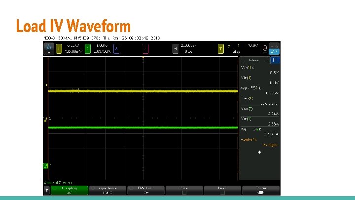
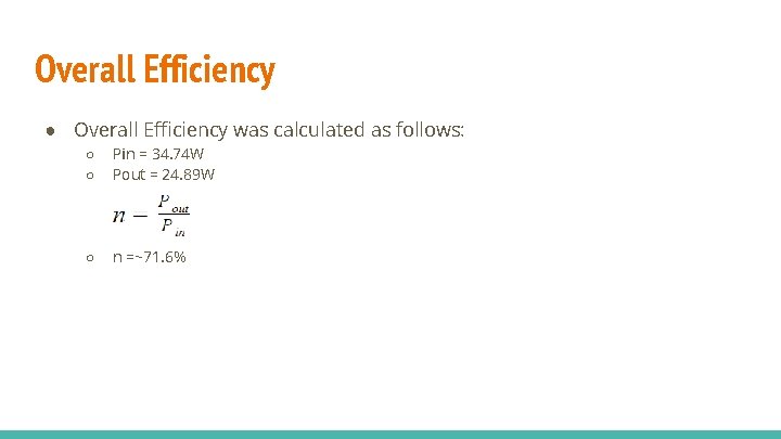
Rectifier Circuit with LC Filter Requirements ● Rectifier Circuit and LC filter had the following requirements: ○ ○ Make a clean output of 12 V and 3. 33 A for load ■ Within 2% ripple The rectifier handles voltage coming from secondary side coil ■ Verified by stress calculations

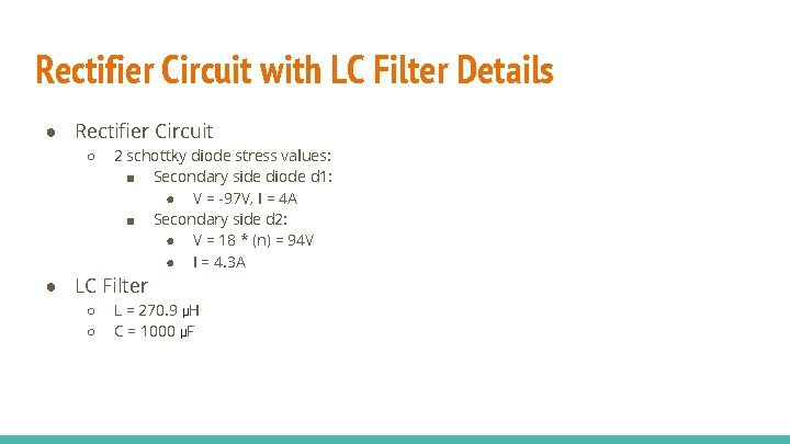
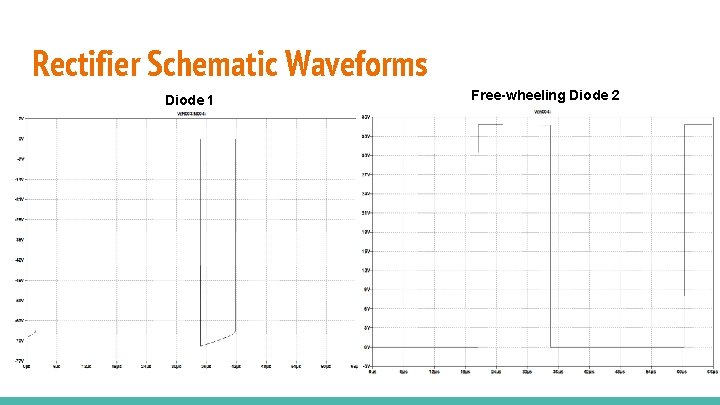
Rectifier Circuit with LC Filter Details ● Rectifier Circuit ○ 2 schottky diode stress values: ■ Secondary side diode d 1: ● V = -97 V, I = 4 A ■ Secondary side d 2: ● V = 18 * (n) = 94 V ● I = 4. 3 A ● LC Filter ○ ○ L = 270. 9 µH C = 1000 µF

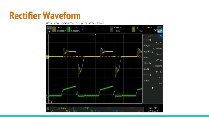
Rectifier Waveform

Rectifier Schematic Waveforms Diode 1 Free-wheeling Diode 2

Load IV Waveform

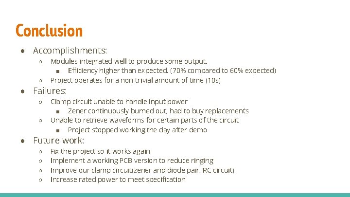
Overall Efficiency ● Overall Efficiency was calculated as follows: ○ ○ Pin = 34. 74 W Pout = 24. 89 W ○ n =~71. 6%

Conclusion ● Accomplishments: ○ ○ Modules integrated well to produce some output. ■ Efficiency higher than expected. (70% compared to 60% expected) Project operates for a non-trivial amount of time (10 s) ● Failures: ○ ○ Clamp circuit unable to handle input power ■ Zener continuously burned out, had to buy replacements Unable to retrieve waveforms for certain parts of the circuit ■ Project stopped working the day after demo ● Future work: ○ ○ Fix the project so it works again Implement a working PCB version to reduce ringing Improve our clamp circuit(zener and diode pair, RC circuit) Increase rated power to meet specification