The VonNeumann Computer Model Partitioning of the computing
![RTN Statement Examples MD ¬ M[MA] – Memory locations are indicated by square brackets. RTN Statement Examples MD ¬ M[MA] – Memory locations are indicated by square brackets.](https://slidetodoc.com/presentation_image/2374c46e67a551b2491837619da5b764/image-7.jpg)
- Slides: 34

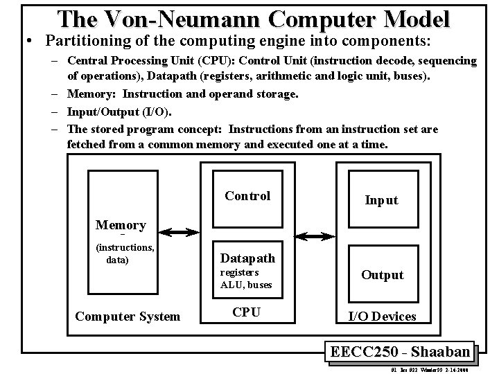
The Von-Neumann Computer Model • Partitioning of the computing engine into components: – Central Processing Unit (CPU): Control Unit (instruction decode, sequencing of operations), Datapath (registers, arithmetic and logic unit, buses). – Memory: Instruction and operand storage. – Input/Output (I/O). – The stored program concept: Instructions from an instruction set are fetched from a common memory and executed one at a time. Control Input Memory (instructions, data) Computer System Datapath registers ALU, buses Output CPU I/O Devices EECC 250 - Shaaban #1 lec #22 Winter 99 2 -16 -2000

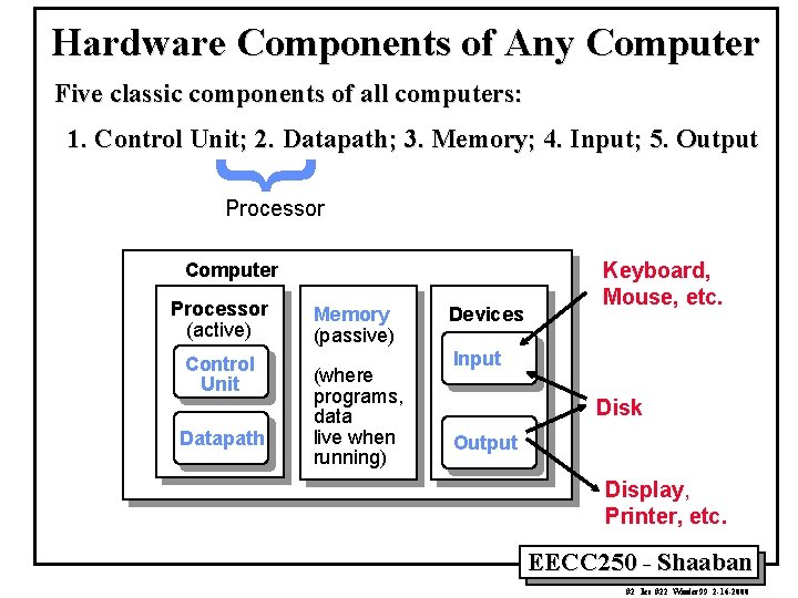
Hardware Components of Any Computer Five classic components of all computers: 1. Control Unit; 2. Datapath; 3. Memory; 4. Input; 5. Output } Processor Computer Processor (active) Control Unit Datapath Memory (passive) (where programs, data live when running) Devices Keyboard, Mouse, etc. Input Disk Output Display, Printer, etc. EECC 250 - Shaaban #2 lec #22 Winter 99 2 -16 -2000

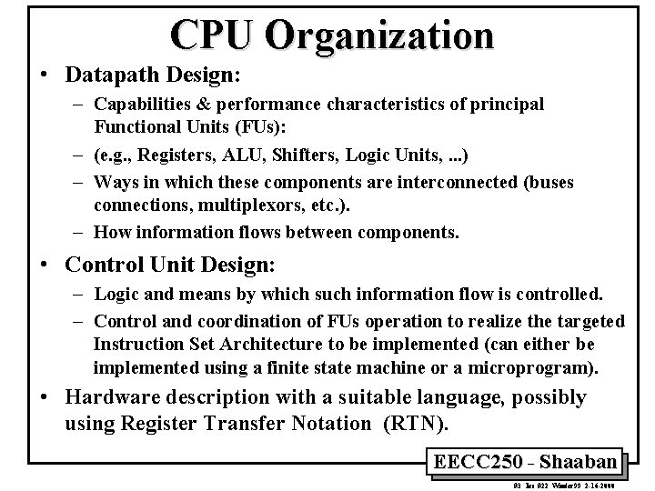
CPU Organization • Datapath Design: – Capabilities & performance characteristics of principal Functional Units (FUs): – (e. g. , Registers, ALU, Shifters, Logic Units, . . . ) – Ways in which these components are interconnected (buses connections, multiplexors, etc. ). – How information flows between components. • Control Unit Design: – Logic and means by which such information flow is controlled. – Control and coordination of FUs operation to realize the targeted Instruction Set Architecture to be implemented (can either be implemented using a finite state machine or a microprogram). • Hardware description with a suitable language, possibly using Register Transfer Notation (RTN). EECC 250 - Shaaban #3 lec #22 Winter 99 2 -16 -2000

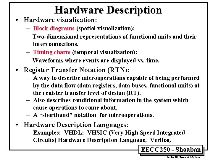
Hardware Description • Hardware visualization: – Block diagrams (spatial visualization): Two-dimensional representations of functional units and their interconnections. – Timing charts (temporal visualization): Waveforms where events are displayed vs. time. • Register Transfer Notation (RTN): – A way to describe microoperations capable of being performed by the data flow (data registers, data buses, functional units) at the register transfer level of design (RT). – Also describes conditional information in the system which cause operations to come about. – A “shorthand” notation for microoperations. • Hardware Description Languages: – Examples: VHDL: VHSIC (Very High Speed Integrated Circuits) Hardware Description Language, Verilog. EECC 250 - Shaaban #4 lec #22 Winter 99 2 -16 -2000

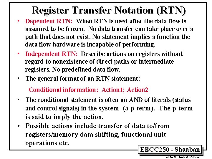
Register Transfer Notation (RTN) • Dependent RTN: When RTN is used after the data flow is assumed to be frozen. No data transfer can take place over a path that does not exist. No statement implies a function the data flow hardware is incapable of performing. • Independent RTN: Describe actions on registers without regard to nonexistence of direct paths or intermediate registers. No predefined data flow. • The general format of an RTN statement: Conditional information: Action 1; Action 2 • The conditional statement is often an AND of literals (status and control signals) in the system (a p-term). The p-term is said to imply the action. • Possible actions include transfer of data to/from registers/memory data shifting, functional unit operations etc. EECC 250 - Shaaban #5 lec #22 Winter 99 2 -16 -2000

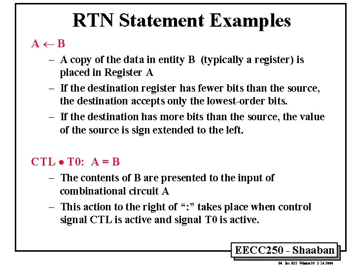
RTN Statement Examples A¬B – A copy of the data in entity B (typically a register) is placed in Register A – If the destination register has fewer bits than the source, the destination accepts only the lowest-order bits. – If the destination has more bits than the source, the value of the source is sign extended to the left. CTL · T 0: A = B – The contents of B are presented to the input of combinational circuit A – This action to the right of “: ” takes place when control signal CTL is active and signal T 0 is active. EECC 250 - Shaaban #6 lec #22 Winter 99 2 -16 -2000
![RTN Statement Examples MD MMA Memory locations are indicated by square brackets RTN Statement Examples MD ¬ M[MA] – Memory locations are indicated by square brackets.](https://slidetodoc.com/presentation_image/2374c46e67a551b2491837619da5b764/image-7.jpg)
RTN Statement Examples MD ¬ M[MA] – Memory locations are indicated by square brackets. – Means the memory data register receives the contents of the main memory (M) as addressed from the Memory Address (MA) register. AC(0), AC(1), AC(2), AC(3) – – – Register fields are indicated by parenthesis. The concatenation operation is indicated by a comma. Bit AC(0) is bit 0 of the accumulator AC The above expression means AC bits 0, 1, 2, 3 More commonly represented by AC(0 -3) E · T 3: CLRWRITE – The control signal CLRWRITE is activated when the condition E · T 3 is active. EECC 250 - Shaaban #7 lec #22 Winter 99 2 -16 -2000

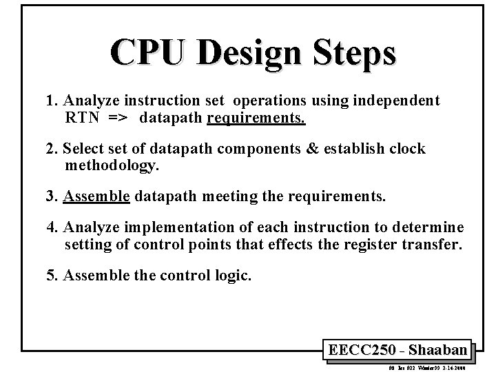
CPU Design Steps 1. Analyze instruction set operations using independent RTN => datapath requirements. 2. Select set of datapath components & establish clock methodology. 3. Assemble datapath meeting the requirements. 4. Analyze implementation of each instruction to determine setting of control points that effects the register transfer. 5. Assemble the control logic. EECC 250 - Shaaban #8 lec #22 Winter 99 2 -16 -2000

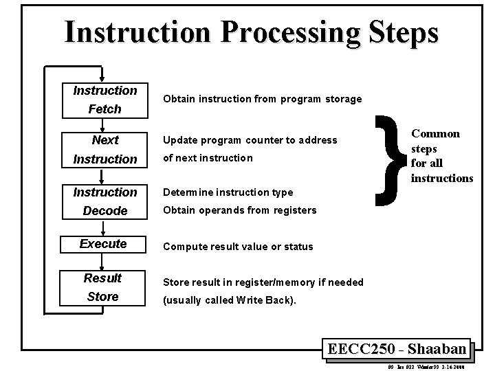
Instruction Processing Steps Instruction Fetch Next Obtain instruction from program storage Update program counter to address Instruction of next instruction Instruction Determine instruction type Decode Obtain operands from registers Execute Compute result value or status Result Store result in register/memory if needed Store (usually called Write Back). } Common steps for all instructions EECC 250 - Shaaban #9 lec #22 Winter 99 2 -16 -2000

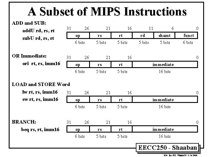
A Subset of MIPS Instructions ADD and SUB: add. U rd, rs, rt sub. U rd, rs, rt 31 OR Immediate: ori rt, rs, imm 16 31 26 op 6 bits LOAD and STORE Word lw rt, rs, imm 16 31 26 sw rt, rs, imm 16 op 6 bits BRANCH: beq rs, rt, imm 16 31 26 op 6 bits 21 rs 5 bits 16 rt 5 bits 11 rd 5 bits 6 shamt 5 bits 16 rt 5 bits immediate 16 bits 0 immediate 16 bits 16 rt 5 bits funct 6 bits 0 16 rt 5 bits 0 0 immediate 16 bits EECC 250 - Shaaban #10 lec #22 Winter 99 2 -16 -2000

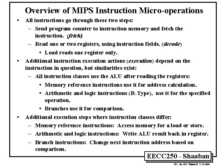
Overview of MIPS Instruction Micro-operations • • • All instructions go through these two steps: – Send program counter to instruction memory and fetch the instruction. (fetch) – Read one or two registers, using instruction fields. (decode) • Load reads one register only. Additional instruction execution actions (execution) depend on the instruction in question, but similarities exist: – All instruction classes use the ALU after reading the registers: • Memory reference instructions use it for address calculation. • Arithmetic and logic instructions (R-Type), use it for the specified operation. • Branches use it for comparison. Additional execution steps where instruction classes differ: – Memory reference instructions: Access memory for a load or store. – Arithmetic and logic instructions: Write ALU result back in register. – Branch instructions: Change next instruction address based on comparison. EECC 250 - Shaaban #11 lec #22 Winter 99 2 -16 -2000

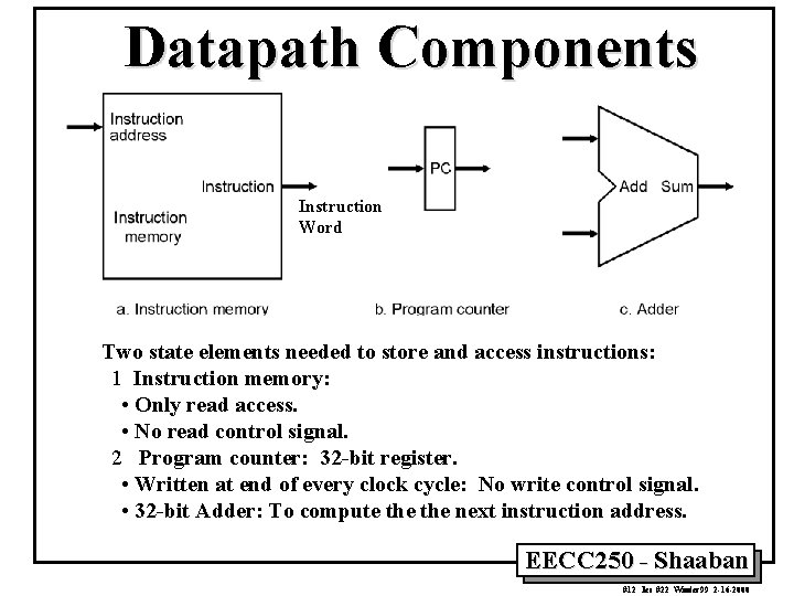
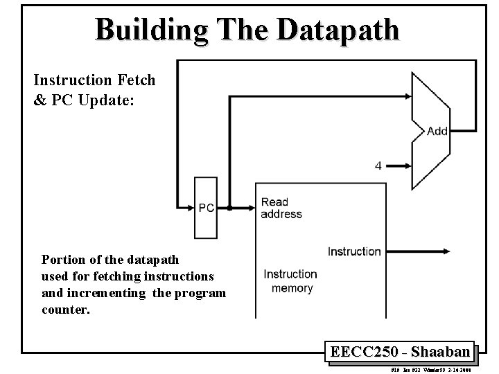
Datapath Components Instruction Word Two state elements needed to store and access instructions: 1 Instruction memory: • Only read access. • No read control signal. 2 Program counter: 32 -bit register. • Written at end of every clock cycle: No write control signal. • 32 -bit Adder: To compute the next instruction address. EECC 250 - Shaaban #12 lec #22 Winter 99 2 -16 -2000

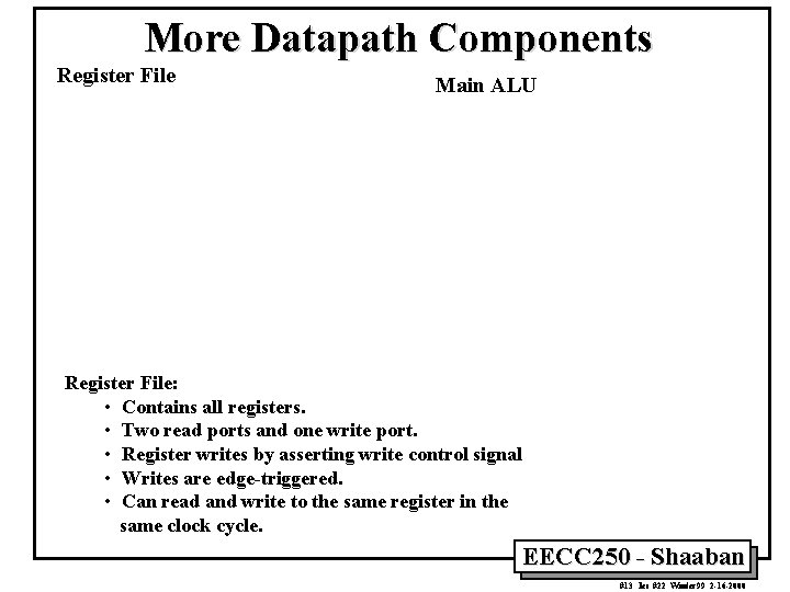
More Datapath Components Register File Main ALU Register File: • Contains all registers. • Two read ports and one write port. • Register writes by asserting write control signal • Writes are edge-triggered. • Can read and write to the same register in the same clock cycle. EECC 250 - Shaaban #13 lec #22 Winter 99 2 -16 -2000

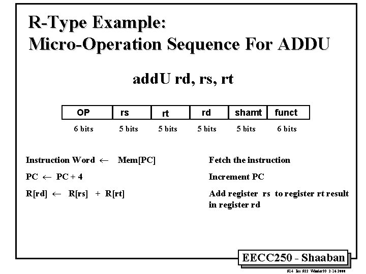
R-Type Example: Micro-Operation Sequence For ADDU add. U rd, rs, rt OP 6 bits Instruction Word ¬ rs 5 bits Mem[PC] rt rd shamt funct 5 bits 6 bits Fetch the instruction PC ¬ PC + 4 Increment PC R[rd] ¬ R[rs] + R[rt] Add register rs to register rt result in register rd EECC 250 - Shaaban #14 lec #22 Winter 99 2 -16 -2000

Building The Datapath Instruction Fetch & PC Update: Portion of the datapath used for fetching instructions and incrementing the program counter. EECC 250 - Shaaban #15 lec #22 Winter 99 2 -16 -2000

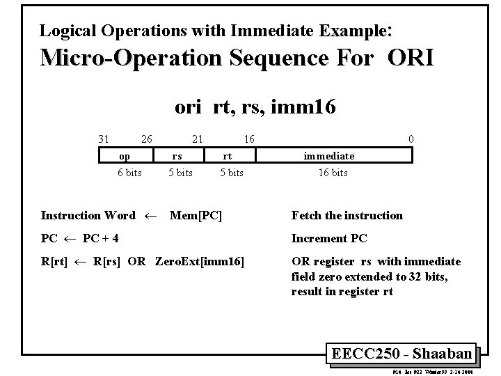
Logical Operations with Immediate Example: Micro-Operation Sequence For ORI ori rt, rs, imm 16 31 26 op 6 bits Instruction Word ¬ 21 rs 5 bits 16 rt 5 bits Mem[PC] 0 immediate 16 bits Fetch the instruction PC ¬ PC + 4 Increment PC R[rt] ¬ R[rs] OR Zero. Ext[imm 16] OR register rs with immediate field zero extended to 32 bits, result in register rt EECC 250 - Shaaban #16 lec #22 Winter 99 2 -16 -2000

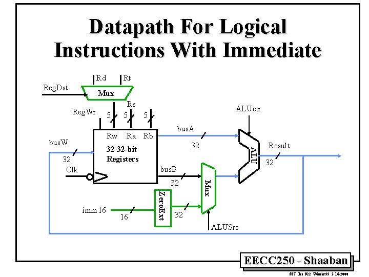
Datapath For Logical Instructions With Immediate Rd Reg. Dst Rt Mux Reg. Wr 5 Rw bus. W Rs 5 5 ALUctr bus. A Ra Rb 32 Clk ALU 32 32 32 -bit Registers bus. B 16 Zero. Ext imm 16 32 Mux 32 Result 32 ALUSrc EECC 250 - Shaaban #17 lec #22 Winter 99 2 -16 -2000

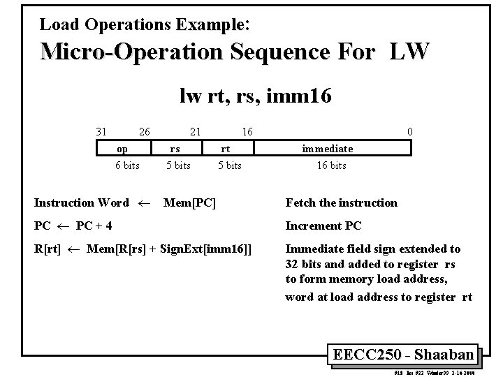
Load Operations Example: Micro-Operation Sequence For LW lw rt, rs, imm 16 31 26 op 6 bits Instruction Word ¬ 21 rs 5 bits 16 rt 5 bits Mem[PC] 0 immediate 16 bits Fetch the instruction PC ¬ PC + 4 Increment PC R[rt] ¬ Mem[R[rs] + Sign. Ext[imm 16]] Immediate field sign extended to 32 bits and added to register rs to form memory load address, word at load address to register rt EECC 250 - Shaaban #18 lec #22 Winter 99 2 -16 -2000

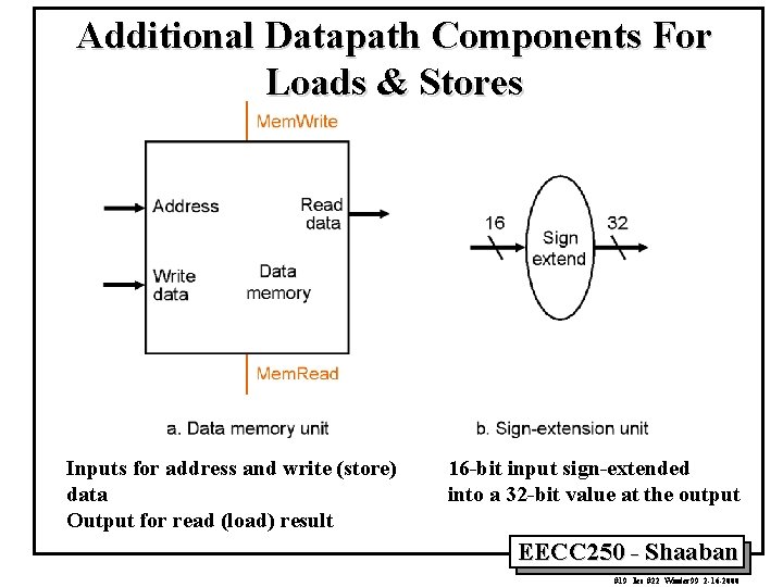
Additional Datapath Components For Loads & Stores Inputs for address and write (store) data Output for read (load) result 16 -bit input sign-extended into a 32 -bit value at the output EECC 250 - Shaaban #19 lec #22 Winter 99 2 -16 -2000

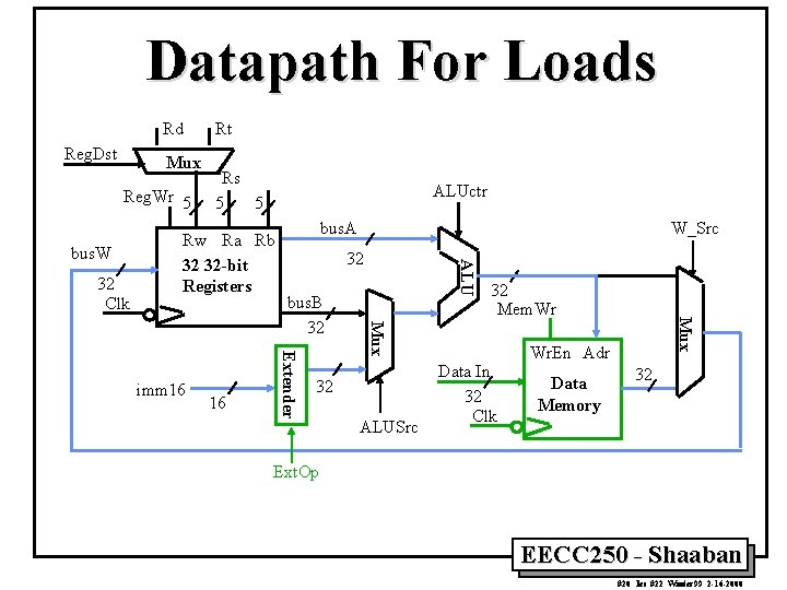
Datapath For Loads Rd Reg. Dst Mux Reg. Wr 5 32 Clk Rs 5 5 ALUctr Rw Ra Rb 32 32 -bit Registers 32 Mem. Wr 32 ALUSrc Data In 32 Clk Mux bus. B 32 Mux 16 W_Src 32 Extender imm 16 bus. A ALU bus. W Rt Wr. En Adr Data Memory 32 Ext. Op EECC 250 - Shaaban #20 lec #22 Winter 99 2 -16 -2000

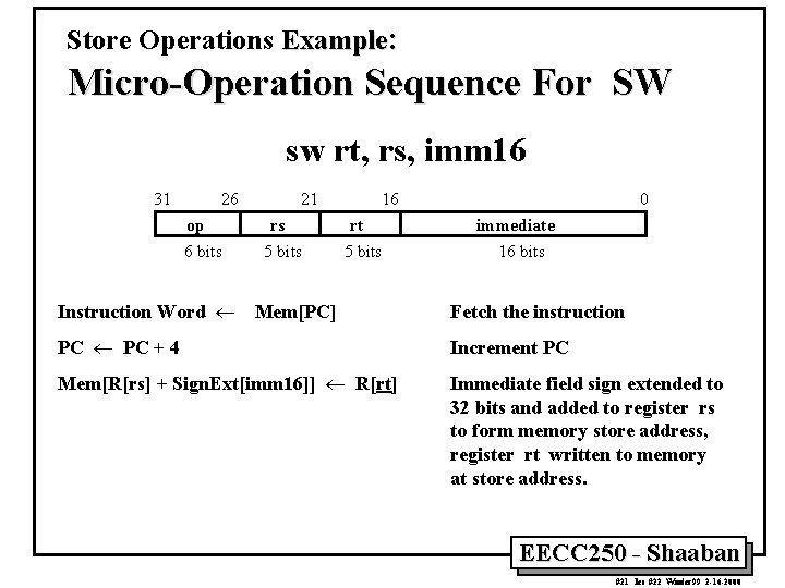
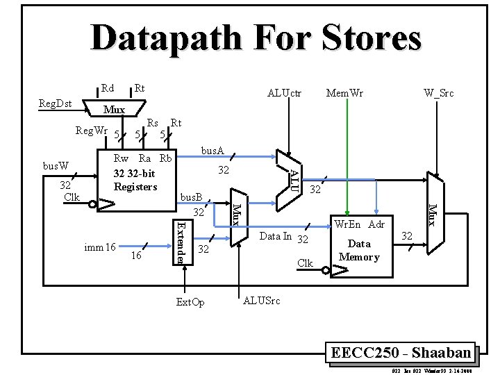
Store Operations Example: Micro-Operation Sequence For SW sw rt, rs, imm 16 31 26 op 6 bits Instruction Word ¬ 21 rs 5 bits 16 rt 5 bits Mem[PC] 0 immediate 16 bits Fetch the instruction PC ¬ PC + 4 Increment PC Mem[R[rs] + Sign. Ext[imm 16]] ¬ R[rt] Immediate field sign extended to 32 bits and added to register rs to form memory store address, register rt written to memory at store address. EECC 250 - Shaaban #21 lec #22 Winter 99 2 -16 -2000

Datapath For Stores Rd Reg. Dst Rt ALUctr Mem. Wr W_Src Mux Reg. Wr 5 32 Clk 5 Rt Rw Ra Rb 32 32 -bit Registers 32 Ext. Op 32 Data In 32 Clk Wr. En Adr Data Memory Mux bus. B 32 Mux 16 32 Extender imm 16 bus. A ALU bus. W 5 Rs 32 ALUSrc EECC 250 - Shaaban #22 lec #22 Winter 99 2 -16 -2000

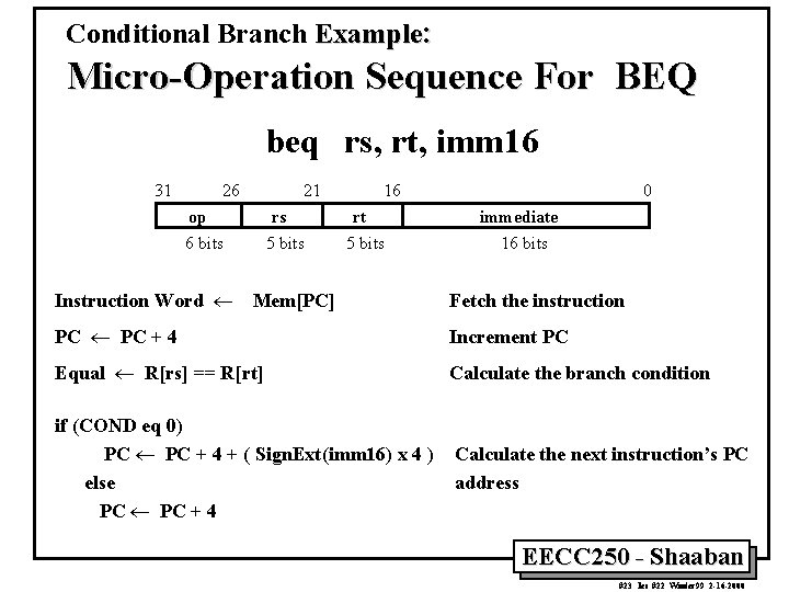
Conditional Branch Example: Micro-Operation Sequence For BEQ beq rs, rt, imm 16 31 26 21 op 6 bits Instruction Word ¬ rs 5 bits 16 rt 5 bits Mem[PC] 0 immediate 16 bits Fetch the instruction PC ¬ PC + 4 Increment PC Equal ¬ R[rs] == R[rt] Calculate the branch condition if (COND eq 0) PC ¬ PC + 4 + ( Sign. Ext(imm 16) x 4 ) else PC ¬ PC + 4 Calculate the next instruction’s PC address EECC 250 - Shaaban #23 lec #22 Winter 99 2 -16 -2000

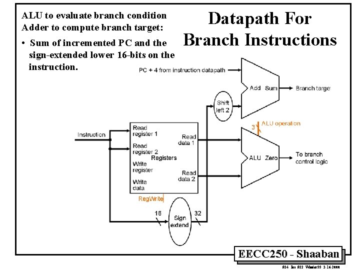
ALU to evaluate branch condition Adder to compute branch target: • Sum of incremented PC and the sign-extended lower 16 -bits on the instruction. Datapath For Branch Instructions EECC 250 - Shaaban #24 lec #22 Winter 99 2 -16 -2000

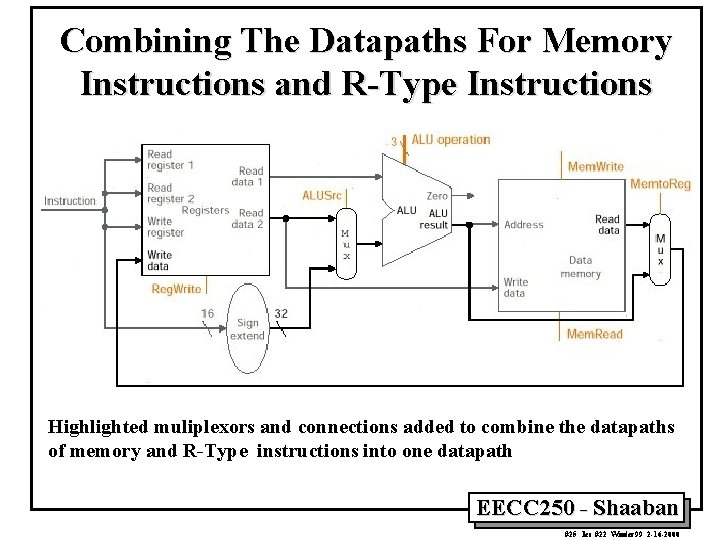
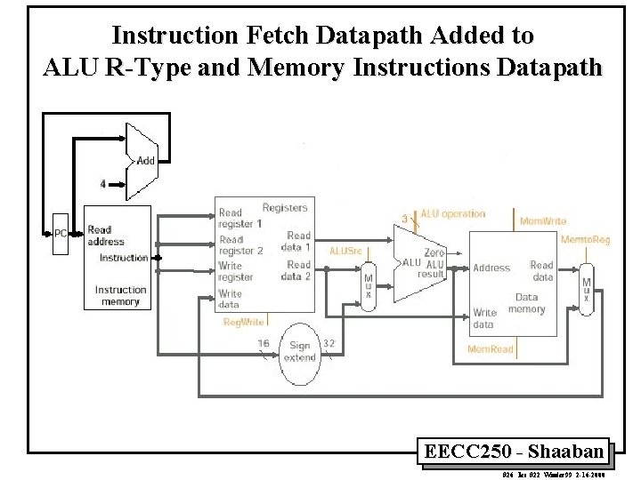
Combining The Datapaths For Memory Instructions and R-Type Instructions Highlighted muliplexors and connections added to combine the datapaths of memory and R-Type instructions into one datapath EECC 250 - Shaaban #25 lec #22 Winter 99 2 -16 -2000

Instruction Fetch Datapath Added to ALU R-Type and Memory Instructions Datapath EECC 250 - Shaaban #26 lec #22 Winter 99 2 -16 -2000

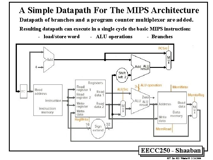
A Simple Datapath For The MIPS Architecture Datapath of branches and a program counter multiplexor are added. Resulting datapath can execute in a single cycle the basic MIPS instruction: - load/store word - ALU operations - Branches EECC 250 - Shaaban #27 lec #22 Winter 99 2 -16 -2000

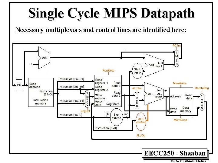
Single Cycle MIPS Datapath Necessary multiplexors and control lines are identified here: EECC 250 - Shaaban #28 lec #22 Winter 99 2 -16 -2000

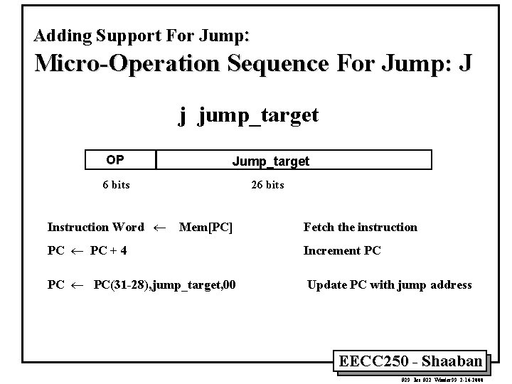
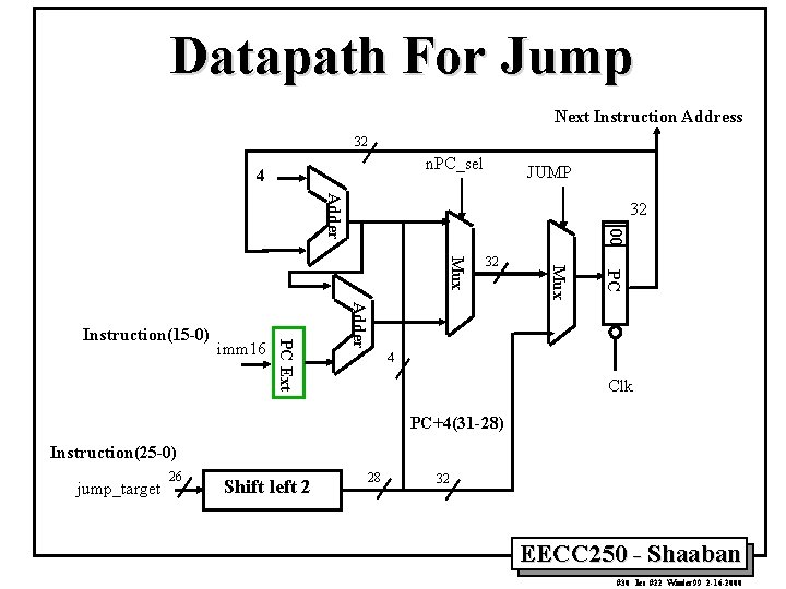
Adding Support For Jump: Micro-Operation Sequence For Jump: J j jump_target OP Jump_target 6 bits 26 bits Instruction Word ¬ Mem[PC] Fetch the instruction PC ¬ PC + 4 Increment PC PC ¬ PC(31 -28), jump_target, 00 Update PC with jump address EECC 250 - Shaaban #29 lec #22 Winter 99 2 -16 -2000

Datapath For Jump Next Instruction Address 32 n. PC_sel 4 JUMP Adder 00 32 PC Mux Adder imm 16 PC Ext Instruction(15 -0) 32 4 Clk PC+4(31 -28) Instruction(25 -0) jump_target 26 Shift left 2 28 32 EECC 250 - Shaaban #30 lec #22 Winter 99 2 -16 -2000

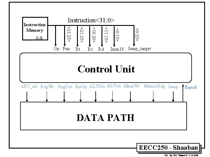
<0: 25> Rd <0: 15> Rs <11: 15> Rt <16: 20> Op Fun <21: 25> Adr Instruction<31: 0> <21: 25> Instruction Memory Imm 16 Jump_target Control Unit n. PC_sel Reg. Wr Reg. Dst Ext. Op ALUSrc ALUctr Mem. Wr Memto. Reg Jump Equal DATA PATH EECC 250 - Shaaban #31 lec #22 Winter 99 2 -16 -2000

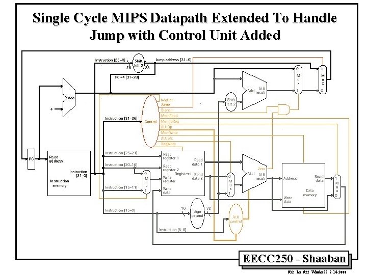
Single Cycle MIPS Datapath Extended To Handle Jump with Control Unit Added EECC 250 - Shaaban #32 lec #22 Winter 99 2 -16 -2000

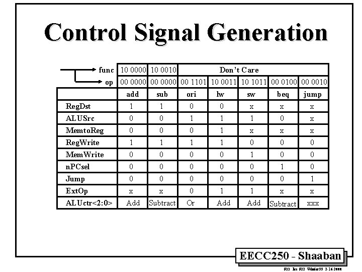
Control Signal Generation func 10 0000 10 0010 Don’t Care op 00 0000 00 1101 10 0011 10 1011 00 0100 00 0010 add sub ori lw sw beq jump 1 1 0 0 x x x Reg. Dst ALUSrc Memto. Reg. Write Mem. Write n. PCsel Jump Ext. Op ALUctr<2: 0> 0 0 1 0 1 0 1 1 1 0 1 x 0 1 0 x 0 0 x Add 0 0 x Subtract 0 0 0 Or 0 0 1 Add 1 0 x 0 1 x xxx Subtract EECC 250 - Shaaban #33 lec #22 Winter 99 2 -16 -2000

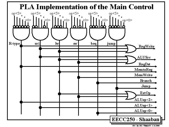
PLA Implementation of the Main Control. . op<5> <0> R-type . . op<5> <0> ori . . op<5> <0> lw . . op<5> <0> sw . . op<5> <0> beq op<0> jump Reg. Write ALUSrc Reg. Dst Memto. Reg Mem. Write Branch Jump Ext. Op ALUop<2> ALUop<1> ALUop<0> EECC 250 - Shaaban #34 lec #22 Winter 99 2 -16 -2000