Status on longwavelength In P waveguide heterojunction phototransistors
- Slides: 34

Status on long-wavelength In. P waveguide heterojunction phototransistors Samuel Dupont, Vincent Magnin, Manuel Fendler, Filippe Jorge, Sophie Maricot, Jean-Pierre Vilcot, Joseph Harari, Didier Decoster Institut d'Electronique de Microélectronique et de Nanotechnologie, UMR CNRS 8520 Université des Sciences et Technologies de Lille 59 652 Villeneuve d’Ascq France

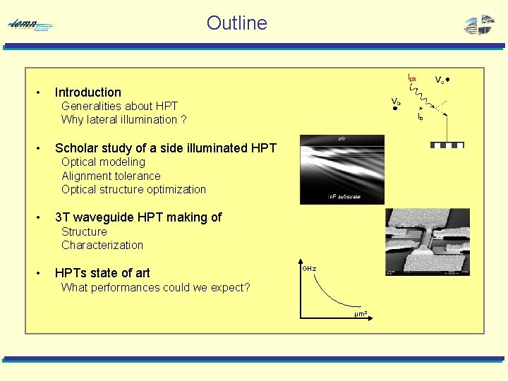
Outline • Introduction Generalities about HPT Why lateral illumination ? • Scholar study of a side illuminated HPT Optical modeling Alignment tolerance Optical structure optimization • 3 T waveguide HPT making of Structure Characterization • HPTs state of art GHz What performances could we expect? µm²

Heterostructure phototransistor • • Offers gain compared to PIN-diode or UTC Good noise performances (/ APD) Compatible with HBT fabrication process Several configurations: – Top / substrate / side illumination – 2 T / 3 T • Specific applications: injection locked oscillators, clock recovery setups…

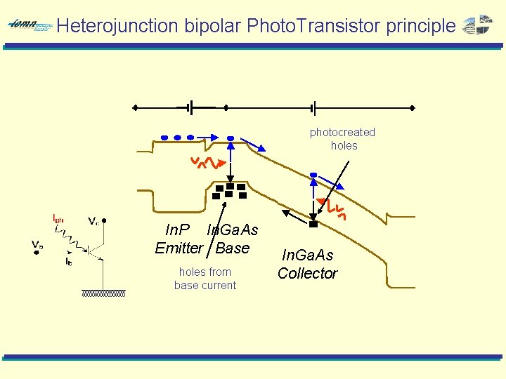
Heterojunction bipolar Photo. Transistor principle photocreated holes In. P In. Ga. As Emitter Base holes from base current In. Ga. As Collector

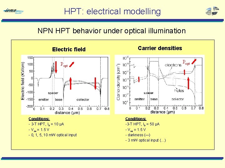
HPT: electrical modelling NPN HPT behavior under optical illumination Electric field Carrier densities Popt Conditions: - 3 -T HPT, Ib = 10 µA - Vce = 1. 5 V - 0, 1, 5, 10 m. W optical input Conditions: -3 -T HPT, Ib = 50 µA - Vce = 1. 5 V - darkness (—) - 3 m. W optical input ( )

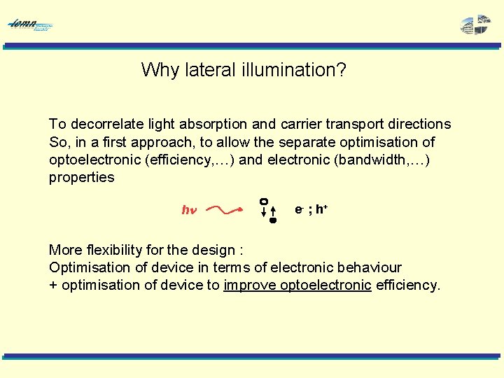
Why lateral illumination? To decorrelate light absorption and carrier transport directions So, in a first approach, to allow the separate optimisation of optoelectronic (efficiency, …) and electronic (bandwidth, …) properties hn e- ; h + More flexibility for the design : Optimisation of device in terms of electronic behaviour + optimisation of device to improve optoelectronic efficiency.

• Introduction • Scholar study Optical modeling Optical structure optimization • 3 T HPT making of Structure Characterization • HPT state of art • Side illumination requires optical guiding properties of the device • Need a specific design to optimize the coupling efficiency Þ BPM simulations of the structure

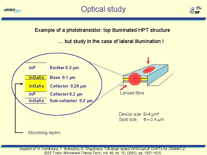
Optical study Example of a phototransistor: top illuminated HPT structure … but study in the case of lateral illumination ! In. P Emitter 0. 3 µm In. Ga. As Base 0. 1 µm In. Ga. As Collector 0. 28 µm In. P Collector 0. 2 µm In. Ga. As Sub-collector 0. 2 µm Lensed fibre Device size: 6 x 4 µm² Spot size: F = 2. 4 mm Absorbing layers Inspired of: H. Kamitsuna, Y. Matsuoka, N. Shigekawa, “Ultrahigh-speed In. P/In. Ga. As. P DHPTs for OEMMICs”, IEEE Trans. Microwave Theory Tech. , vol. 49, no. 10, (2001), pp. 1921 -1925.

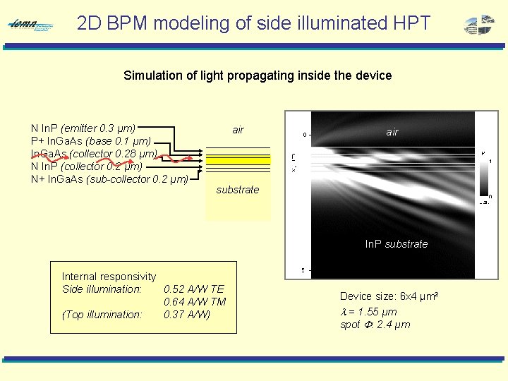
2 D BPM modeling of side illuminated HPT Simulation of light propagating inside the device N In. P (emitter 0. 3 µm) P+ In. Ga. As (base 0. 1 µm) In. Ga. As (collector 0. 28 µm) N In. P (collector 0. 2 µm) N+ In. Ga. As (sub-collector 0. 2 µm) air substrate In. P substrate Internal responsivity Side illumination: 0. 52 A/W TE 0. 64 A/W TM (Top illumination: 0. 37 A/W) Device size: 6 x 4 µm² l = 1. 55 µm spot F: 2. 4 µm

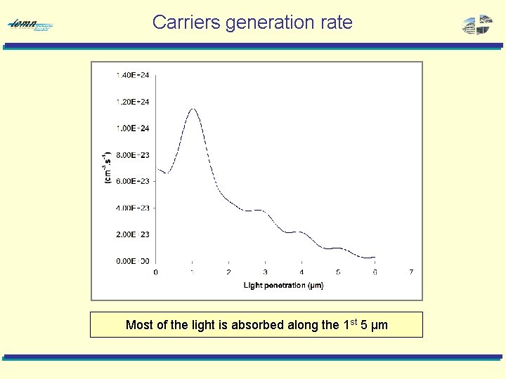
Carriers generation rate Most of the light is absorbed along the 1 st 5 µm

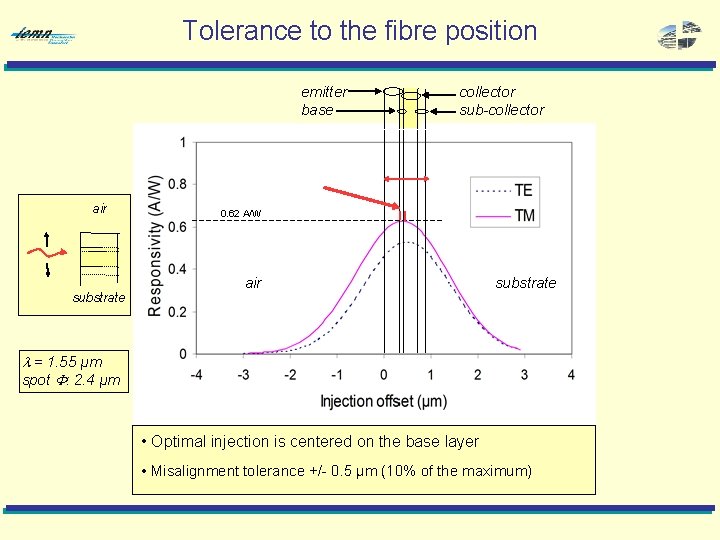
Tolerance to the fibre position emitter base air substrate collector sub-collector 0. 62 A/W air substrate l = 1. 55 µm spot F: 2. 4 µm • Optimal injection is centered on the base layer • Misalignment tolerance +/- 0. 5 µm (10% of the maximum)

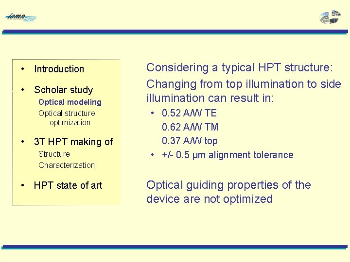
• Introduction • Scholar study Optical modeling Optical structure optimization • 3 T HPT making of Structure Characterization • HPT state of art Considering a typical HPT structure: Changing from top illumination to side illumination can result in: • 0. 52 A/W TE 0. 62 A/W TM 0. 37 A/W top • +/- 0. 5 µm alignment tolerance Optical guiding properties of the device are not optimized

• Introduction • Scholar study Optical modeling Optical structure optimizations • 3 T HPT making of Structure Characterizations • HPT state of art • What do we want ? A more efficient light collection • How to get it ? Get a better light confinement Þ Add a confinement layer

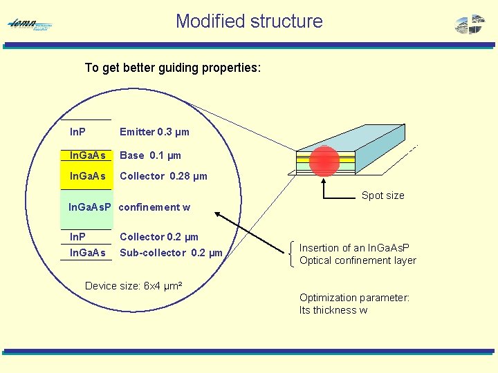
Modified structure To get better guiding properties: In. P Emitter 0. 3 µm In. Ga. As Base 0. 1 µm In. Ga. As Collector 0. 28 µm Spot size In. Ga. As. P confinement w In. P Collector 0. 2 µm In. Ga. As Sub-collector 0. 2 µm Insertion of an In. Ga. As. P Optical confinement layer Device size: 6 x 4 µm² Optimization parameter: Its thickness w

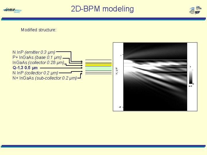
2 D-BPM modeling Modified structure: N In. P (emitter 0. 3 µm) P+ In. Ga. As (base 0. 1 µm) In. Ga. As (collector 0. 28 µm) Q-1. 3 0. 5 µm N In. P (collector 0. 2 µm) N+ In. Ga. As (sub-collector 0. 2 µm)

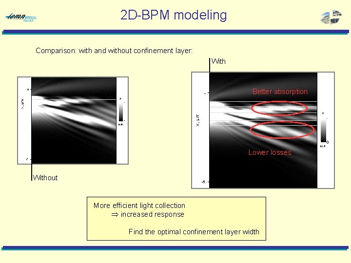
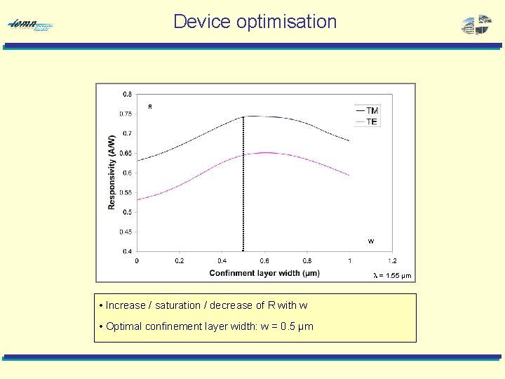
2 D-BPM modeling Comparison: with and without confinement layer: With Better absorption Lower losses Without More efficient light collection Þ increased response Find the optimal confinement layer width

Device optimisation R W l = 1. 55 µm • Increase / saturation / decrease of R with w • Optimal confinement layer width: w = 0. 5 µm

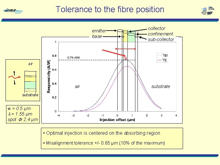
Tolerance to the fibre position emitter base collector confinement sub-collector 0. 74 A/W air substrate w = 0. 5 µm l = 1. 55 µm spot F: 2. 4 µm • Optimal injection is centered on the absorbing region • Misalignment tolerance +/- 0. 65 µm (10% of the maximum)

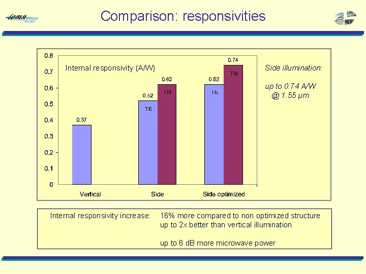
Comparison: responsivities Internal responsivity (A/W) Side illumination: up to 0. 74 A/W @ 1. 55 µm Internal responsivity increase: 16% more compared to non optimized structure up to 2 x better than vertical illumination up to 6 d. B more microwave power

• Introduction • Scholar study Optical modeling Alignment tolerance Optical structure optimization • Side illumination is more efficient • Optimized structure gives about twice the responsivity (with the same absorbing layers) • 3 T HPT making of Structure Characterization • HPT state of art Þ 6 d. B more microwave power

• Introduction • Scholar study Optical modeling Alignment tolerance Optical structure optimization • 3 T HPT making of Structure Characterization • HPT state of art • Light collection: Can we find more efficient structures ? ÞThicker absorbing layer ÞThicker confinement layer (not without consequences on bandwidth!)

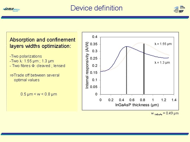
Device definition Absorption and confinement layers widths optimization: l = 1. 55 µm -Two polarizations -Two l: 1. 55 µm ; 1. 3 µm - Two fibres F: cleaved ; lensed l = 1. 3 µm ÞTrade off between several optimal values 0. 5 µm < w < 0. 8 µm w In. Ga. As = 0. 49 µm

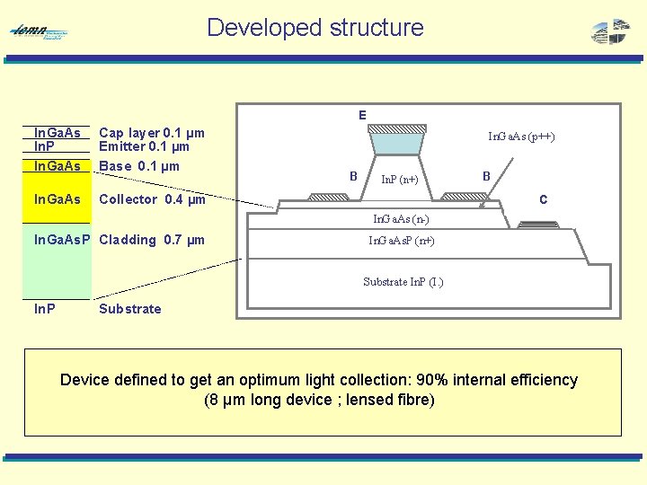
Developed structure E In. Ga. As In. P Cap layer 0. 1 µm Emitter 0. 1 µm In. Ga. As Base 0. 1 µm In. Ga. As (p++) B In. P (n+) Collector 0. 4 µm B C In. Ga. As (n-) In. Ga. As. P Cladding 0. 7 µm In. Ga. As. P (n+) Substrate In. P (I. ) In. P Substrate Device defined to get an optimum light collection: 90% internal efficiency (8 µm long device ; lensed fibre)

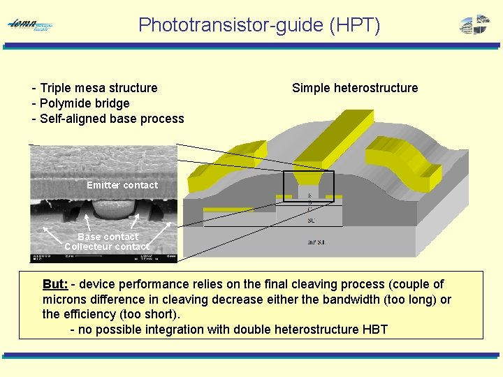
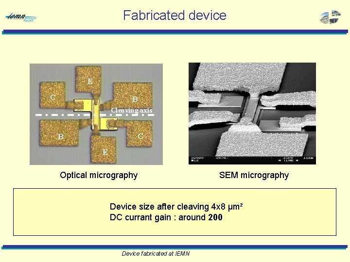
Phototransistor-guide (HPT) - Triple mesa structure - Polymide bridge - Self-aligned base process Simple heterostructure Emitter contact Base contact Collecteur contact But: - device performance relies on the final cleaving process (couple of microns difference in cleaving decrease either the bandwidth (too long) or the efficiency (too short). - no possible integration with double heterostructure HBT

Fabricated device E C B Cleaving axis C B E Optical micrography SEM micrography Device size after cleaving 4 x 8 µm² DC currant gain : around 200 Device fabricated at IEMN

• Introduction • Scholar study Optical modeling Alignment tolerance Optical structure optimization • 3 T HPT making of Structure Characterization • HPT state of art • S parameters extraction – ft, fmax – equivalent model • Opto-microwave parameters – optical fc

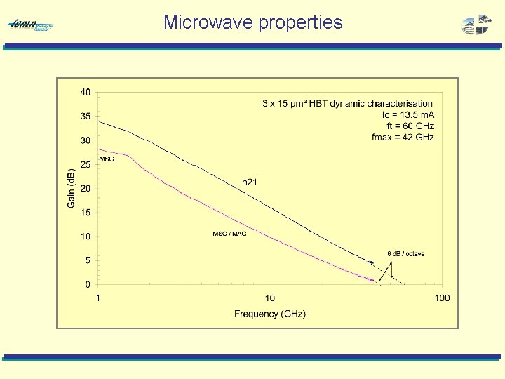
Microwave properties

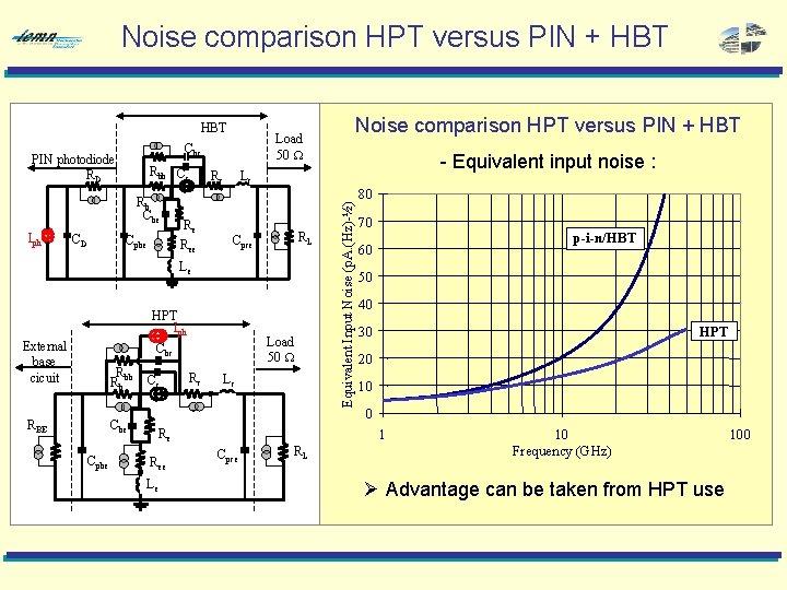
Noise comparison HPT versus PIN + HBT Cbc Rbb Cc Rb Cbe CD Cpbe Re Ree RL Cpce HPT Iph Load 50 W Cbc R Rb bb Cbe RBE Cpbe Cc Rc Lc Re Ree Le - Equivalent input noise : Lc Rc Le External base cicuit Noise comparison HPT versus PIN + HBT Equivalent Input Noise (p. A. (Hz)-½) PIN photodiode RD Iph Load 50 W 80 70 p-i-n/HBT 60 50 40 HPT 30 20 10 0 1 Cpce RL 10 Frequency (GHz) Ø Advantage can be taken from HPT use 100

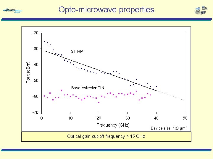
Opto-microwave properties Device size: 4 x 8 µm² Optical gain cut-off frequency > 45 GHz

• Introduction • Scholar study Optical modeling Alignment tolerance Optical structure optimization • 3 T HPT making of Structure Characterization • HPT state of art • 3 T side illuminated HPT: – Trade off optimization (1. 3 µm, 1. 55 µm) – 8 x 4 µm² after cleaving – w. In. Ga. As = 0. 5 µm – w. In. Ga. As. P = 0. 7 µm – DC gain: 200 – ft = 60 GHz – fcopt = 45 GHz

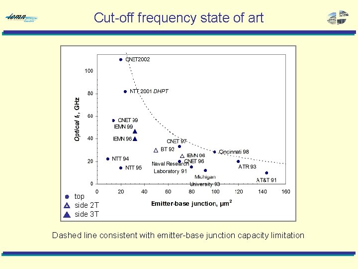
• Introduction • Scholar study Optical modeling Alignment tolerance Optical structure optimization • 3 T HPT making of Structure Characterization • HPT state of art • Electrical DHBT can go up several hundreds of GHz • BUT: – Optical HPT needs a sufficient absorbing layer – Side illumination requires a confinement layer • However 100 GHz operation has been reported

Cut-off frequency state of art top side 2 T side 3 T Dashed line consistent with emitter-base junction capacity limitation

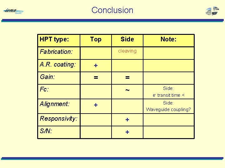
Conclusion HPT type: Top Note: cleaving Fabrication: A. R. coating: + Gain: = Fc: Alignment: Side = ~ Side: e- transit time < Side: Waveguide coupling? + Responsivity: + S/N: +

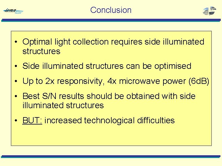
Conclusion • Optimal light collection requires side illuminated structures • Side illuminated structures can be optimised • Up to 2 x responsivity, 4 x microwave power (6 d. B) • Best S/N results should be obtained with side illuminated structures • BUT: increased technological difficulties