Status on TRAMOS Trapping MOS and Dot Pix
- Slides: 19

Status on TRAMOS (Trapping MOS) and Dot. Pix (Quantum Dot Pixel) ongoing developments Nicolas T. Fourches, IRFU/CEA Saclay, 91191 GIF/YVETTE, France E-mail: nicolas. fourches@cea. fr Charles Renard (C 2 N) and G. Hallais, Francois Jomard (GEMAC), Francois Olivié and coworkers (LAAS), the EMIR network (Jannus/Saclay) The purpose of the Dot. Pix project is to design a new kind of pixel for inner vertex detectors arrays with enhanced point-to-point resolution. It is based on a single MOS device, which may allow a resolution below the micron making track reconstruction and vertex determination with an unprecedented accuracy. It comprises a buried gate, which acts as a chargecollecting electrode with memory effect and controls the current of a micron-size n-channel MOS transistor. The design of such a pixel requires the massive use of device simulations. Future e+e- colliders (FCC, ILC) will benefit from this development. I. Motivations for a new pixel design II. How a buried gate can act as collecting electrode III. How it can operate as a memory IV. Designing and fabricating the buried gate V. Simulation results VI. Technological progress VII. Summary and further work 07/10/2020 Nicolas T. Fourches (IRFU) , RD 50 33 rd Workshop , CERN 2018 1

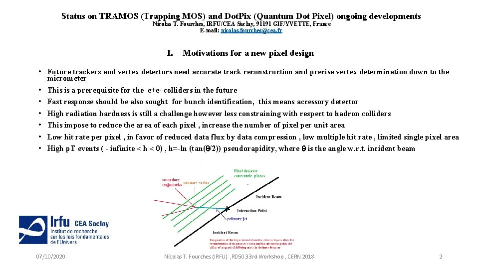
Status on TRAMOS (Trapping MOS) and Dot. Pix (Quantum Dot Pixel) ongoing developments Nicolas T. Fourches, IRFU/CEA Saclay, 91191 GIF/YVETTE, France E-mail: nicolas. fourches@cea. fr I. Motivations for a new pixel design • Future trackers and vertex detectors need accurate track reconstruction and precise vertex determination down to the micrometer • This is a prerequisite for the e+e- colliders in the future • Fast response should be also sought for bunch identification, this means accessory detector • High radiation hardness is still a challenge however less constraining with respect to hadron colliders • This impose to reduce the area of each pixel , increase the number of pixel per unit area • Low hit rate per pixel , in favor of reduced data flux by data compression , low multiple hit rate , limited single pixel area • High p. T events ( - infinite < h < 0) , h=-ln (tan(q/2)) pseudorapidity, where q is the angle w. r. t. incident beam 07/10/2020 Nicolas T. Fourches (IRFU) , RD 50 33 rd Workshop , CERN 2018 2

Status on TRAMOS (Trapping MOS) and Dot. Pix (quantum Dot Pixel) ongoing developments Nicolas T. Fourches, IRFU/CEA Saclay, 91191 GIF/YVETTE, France E-mail: nicolas. fourches@cea. fr I. Motivations for a new pixel design • Classic and modified CMOS pixels, in many cases too slow, need depleted area to be fast (three transistors at least) NIEL tolerance bad in many case due to diffusion the solution has been DMAPS ( with highly resistive substrates) • CCD could be reduced in size but not random addressable. • DEPFET is single device, but should be improved in terms of size • We need a monolithic depleted device with low power consumption, with downscaling possible • Pixel need local readout and memory and a depleted diode, this means many transistors and pixel size > 1 micron squared • We propose to combine every function in a single device pixel : one device + memory in a CMOS compatible process , with a target of 100 nm feature line, and 10 micrometer in depletion layer thickness • Up to now no submicron pixel for charged particle detection has been operating, sizes above 10 x 10 micrometers, this could improve by CMOS downscaling but still need many transistors. 07/10/2020 Nicolas T. Fourches (IRFU) , RD 50 33 rd Workshop , CERN 2018 3

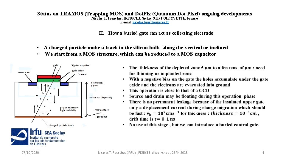
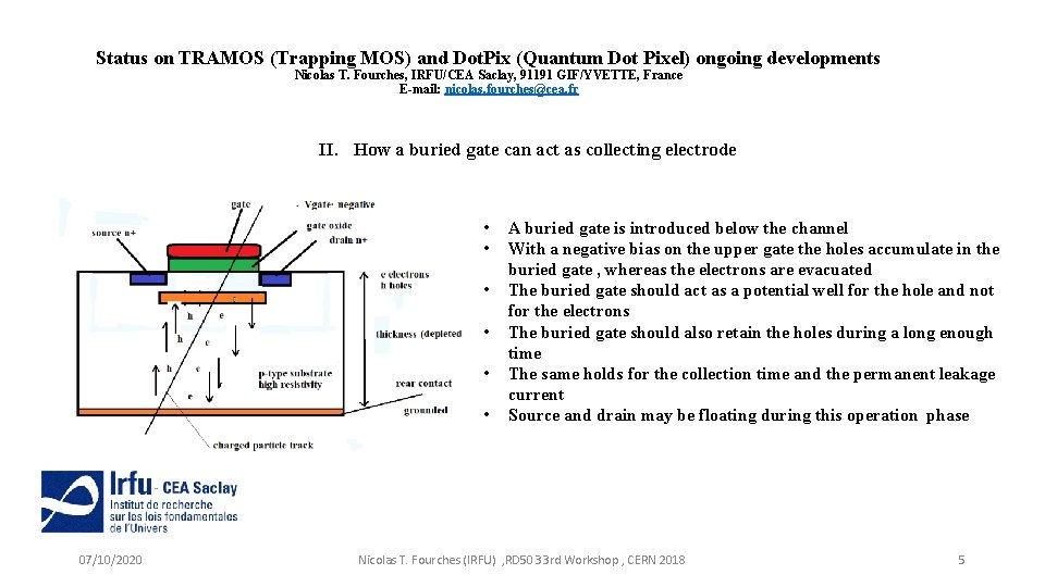
Status on TRAMOS (Trapping MOS) and Dot. Pix (Quantum Dot Pixel) ongoing developments Nicolas T. Fourches, IRFU/CEA Saclay, 91191 GIF/YVETTE, France E-mail: nicolas. fourches@cea. fr II. How a buried gate can act as collecting electrode • A charged particle make a track in the silicon bulk along the vertical or inclined • We start from a MOS structure, which can be reduced to a MOS capacitor 07/10/2020 Nicolas T. Fourches (IRFU) , RD 50 33 rd Workshop , CERN 2018 4

Status on TRAMOS (Trapping MOS) and Dot. Pix (Quantum Dot Pixel) ongoing developments Nicolas T. Fourches, IRFU/CEA Saclay, 91191 GIF/YVETTE, France E-mail: nicolas. fourches@cea. fr II. How a buried gate can act as collecting electrode • • • 07/10/2020 A buried gate is introduced below the channel With a negative bias on the upper gate the holes accumulate in the buried gate , whereas the electrons are evacuated The buried gate should act as a potential well for the hole and not for the electrons The buried gate should also retain the holes during a long enough time The same holds for the collection time and the permanent leakage current Source and drain may be floating during this operation phase Nicolas T. Fourches (IRFU) , RD 50 33 rd Workshop , CERN 2018 5

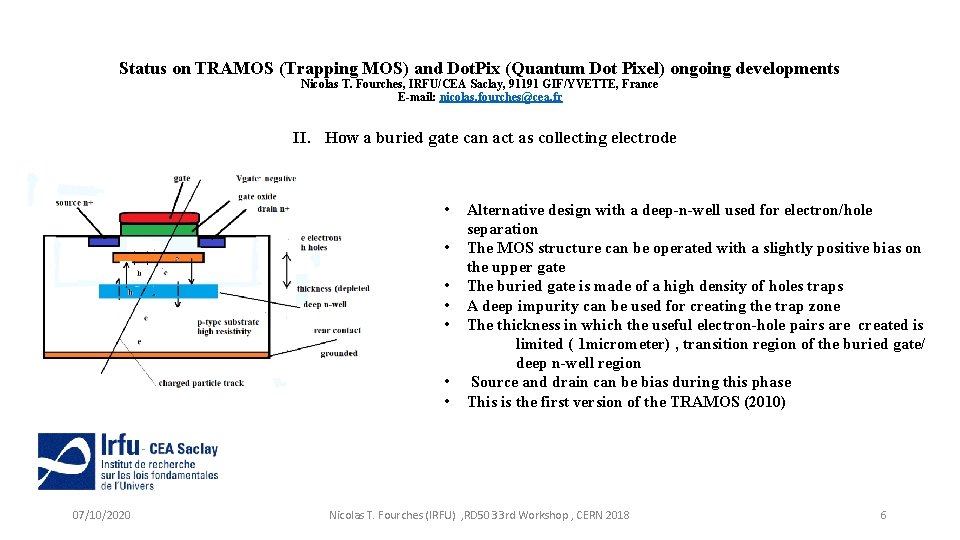
Status on TRAMOS (Trapping MOS) and Dot. Pix (Quantum Dot Pixel) ongoing developments Nicolas T. Fourches, IRFU/CEA Saclay, 91191 GIF/YVETTE, France E-mail: nicolas. fourches@cea. fr II. How a buried gate can act as collecting electrode • • 07/10/2020 Alternative design with a deep-n-well used for electron/hole separation The MOS structure can be operated with a slightly positive bias on the upper gate The buried gate is made of a high density of holes traps A deep impurity can be used for creating the trap zone The thickness in which the useful electron-hole pairs are created is limited ( 1 micrometer) , transition region of the buried gate/ deep n-well region Source and drain can be bias during this phase This is the first version of the TRAMOS (2010) Nicolas T. Fourches (IRFU) , RD 50 33 rd Workshop , CERN 2018 6

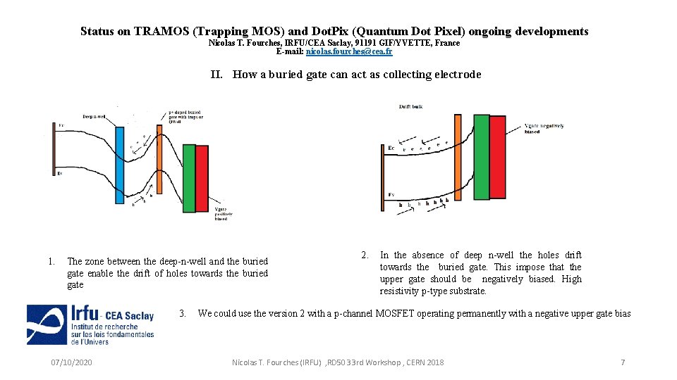
Status on TRAMOS (Trapping MOS) and Dot. Pix (Quantum Dot Pixel) ongoing developments Nicolas T. Fourches, IRFU/CEA Saclay, 91191 GIF/YVETTE, France E-mail: nicolas. fourches@cea. fr II. How a buried gate can act as collecting electrode 1. The zone between the deep-n-well and the buried gate enable the drift of holes towards the buried gate 3. 07/10/2020 2. In the absence of deep n-well the holes drift towards the buried gate. This impose that the upper gate should be negatively biased. High resistivity p-type substrate. We could use the version 2 with a p-channel MOSFET operating permanently with a negative upper gate bias Nicolas T. Fourches (IRFU) , RD 50 33 rd Workshop , CERN 2018 7

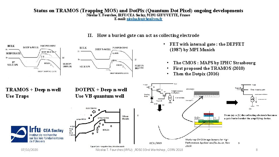
Status on TRAMOS (Trapping MOS) and Dot. Pix (Quantum Dot Pixel) ongoing developments Nicolas T. Fourches, IRFU/CEA Saclay, 91191 GIF/YVETTE, France E-mail: nicolas. fourches@cea. fr II. How a buried gate can act as collecting electrode • FET with internal gate : the DEPFET (1987) by MPI Munich • • • TRAMOS + Deep n-well Use Traps 07/10/2020 The CMOS : MAPS by IPHC Strasbourg First proposed the TRAMOS (2010) Then the Dotpix (2016) DOTPi. X + Deep n-well Use VB quantum well Nicolas T. Fourches (IRFU) , RD 50 33 rd Workshop , CERN 2018 8

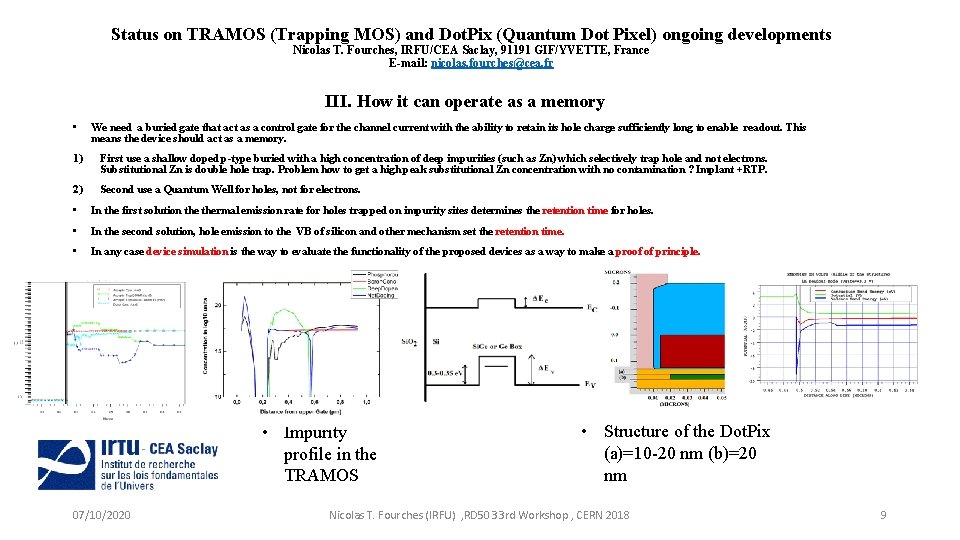
Status on TRAMOS (Trapping MOS) and Dot. Pix (Quantum Dot Pixel) ongoing developments Nicolas T. Fourches, IRFU/CEA Saclay, 91191 GIF/YVETTE, France E-mail: nicolas. fourches@cea. fr III. How it can operate as a memory • We need a buried gate that act as a control gate for the channel current with the ability to retain its hole charge sufficiently long to enable readout. This means the device should act as a memory. 1) First use a shallow doped p-type buried with a high concentration of deep impurities (such as Zn) which selectively trap hole and not electrons. Substitutional Zn is double hole trap. Problem how to get a high peak substitutional Zn concentration with no contamination ? Implant +RTP. 2) Second use a Quantum Well for holes, not for electrons. • In the first solution thermal emission rate for holes trapped on impurity sites determines the retention time for holes. • In the second solution, hole emission to the VB of silicon and other mechanism set the retention time. • In any case device simulation is the way to evaluate the functionality of the proposed devices as a way to make a proof of principle. • Impurity profile in the TRAMOS 07/10/2020 • Structure of the Dot. Pix (a)=10 -20 nm (b)=20 nm Nicolas T. Fourches (IRFU) , RD 50 33 rd Workshop , CERN 2018 9

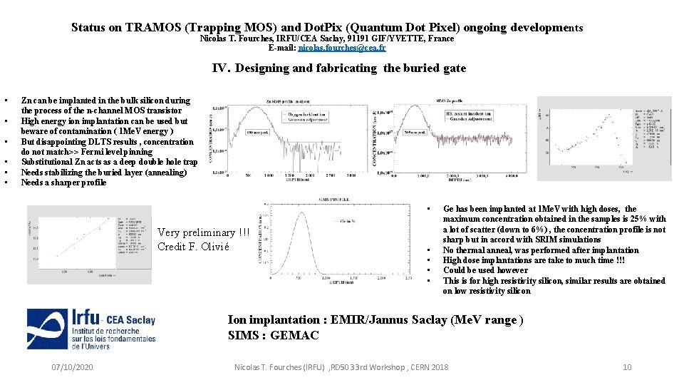
Status on TRAMOS (Trapping MOS) and Dot. Pix (Quantum Dot Pixel) ongoing developments Nicolas T. Fourches, IRFU/CEA Saclay, 91191 GIF/YVETTE, France E-mail: nicolas. fourches@cea. fr IV. Designing and fabricating the buried gate • • • Zn can be implanted in the bulk silicon during the process of the n-channel MOS transistor High energy ion implantation can be used but beware of contamination ( 1 Me. V energy ) But disappointing DLTS results , concentration do not match>> Fermi level pinning Substitutional Zn acts as a deep double hole trap Needs stabilizing the buried layer (annealing) Needs a sharper profile • Very preliminary !!! Credit F. Olivié • • Ge has been implanted at 1 Me. V with high doses, the maximum concentration obtained in the samples is 25% with a lot of scatter (down to 6%) , the concentration profile is not sharp but in accord with SRIM simulations No thermal anneal, was performed after implantation High dose implantations are take to much time !!! Could be used however This is for high resistivity silicon, similar results are obtained on low resistivity silicon Ion implantation : EMIR/Jannus Saclay (Me. V range ) SIMS : GEMAC 07/10/2020 Nicolas T. Fourches (IRFU) , RD 50 33 rd Workshop , CERN 2018 10

Status on TRAMOS (Trapping MOS) and Dot. Pix (Quantum Dot Pixel) ongoing developments Nicolas T. Fourches, IRFU/CEA Saclay, 91191 GIF/YVETTE, France E-mail: nicolas. fourches@cea. fr 07/10/2020 Nicolas T. Fourches (IRFU) , RD 50 33 rd Workshop , CERN 2018 11

Status on TRAMOS (Trapping MOS) and Dot. Pix (Quantum Dot Pixel) ongoing developments Nicolas T. Fourches, IRFU/CEA Saclay, 91191 GIF/YVETTE, France E-mail: nicolas. fourches@cea. fr • 07/10/2020 Nicolas T. Fourches (IRFU) , RD 50 33 rd Workshop , CERN 2018 12

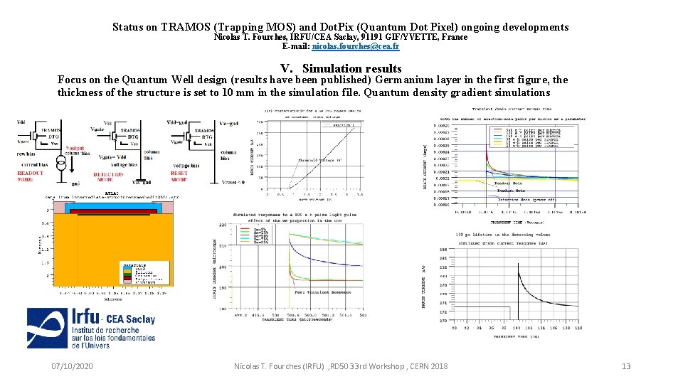
Status on TRAMOS (Trapping MOS) and Dot. Pix (Quantum Dot Pixel) ongoing developments Nicolas T. Fourches, IRFU/CEA Saclay, 91191 GIF/YVETTE, France E-mail: nicolas. fourches@cea. fr V. Simulation results Focus on the Quantum Well design (results have been published) Germanium layer in the first figure, the thickness of the structure is set to 10 mm in the simulation file. Quantum density gradient simulations 07/10/2020 Nicolas T. Fourches (IRFU) , RD 50 33 rd Workshop , CERN 2018 13

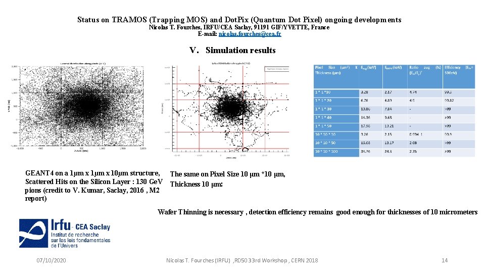
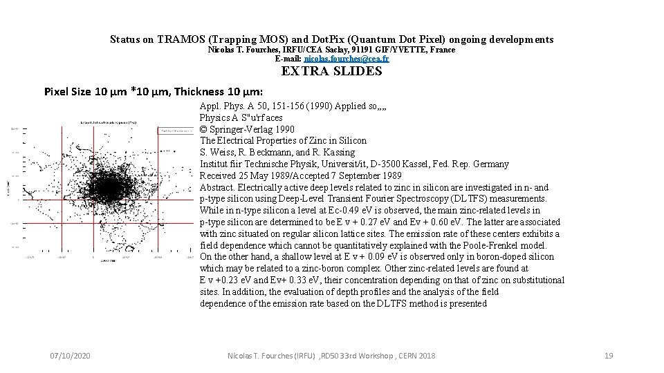
Status on TRAMOS (Trapping MOS) and Dot. Pix (Quantum Dot Pixel) ongoing developments Nicolas T. Fourches, IRFU/CEA Saclay, 91191 GIF/YVETTE, France E-mail: nicolas. fourches@cea. fr V. Simulation results GEANT 4 on a 1µm x 10µm structure, Scattered Hits on the Silicon Layer : 130 Ge. V pions (credit to V. Kumar, Saclay, 2016 , M 2 report) The same on Pixel Size 10 μm *10 μm, Thickness 10 μm: Wafer Thinning is necessary , detection efficiency remains good enough for thicknesses of 10 micrometers 07/10/2020 Nicolas T. Fourches (IRFU) , RD 50 33 rd Workshop , CERN 2018 14

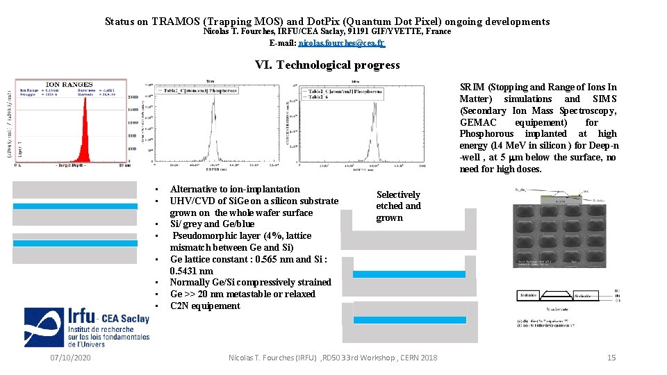
Status on TRAMOS (Trapping MOS) and Dot. Pix (Quantum Dot Pixel) ongoing developments Nicolas T. Fourches, IRFU/CEA Saclay, 91191 GIF/YVETTE, France E-mail: nicolas. fourches@cea. fr VI. Technological progress SRIM (Stopping and Range of Ions In Matter) simulations and SIMS (Secondary Ion Mass Spectroscopy, GEMAC equipement) for Phosphorous implanted at high energy (14 Me. V in silicon ) for Deep-n -well , at 5 mm below the surface, no need for high doses. • • 07/10/2020 Alternative to ion-implantation UHV/CVD of Si. Ge on a silicon substrate grown on the whole wafer surface Si/ grey and Ge/blue Pseudomorphic layer (4%, lattice mismatch between Ge and Si) Ge lattice constant : 0. 565 nm and Si : 0. 5431 nm Normally Ge/Si compressively strained Ge >> 20 nm metastable or relaxed C 2 N equipement Selectively etched and grown Nicolas T. Fourches (IRFU) , RD 50 33 rd Workshop , CERN 2018 15

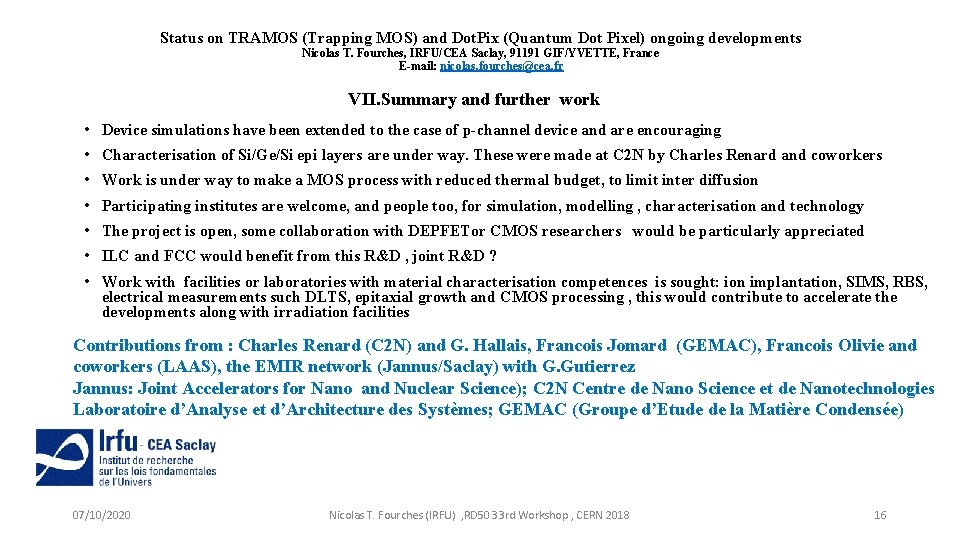
Status on TRAMOS (Trapping MOS) and Dot. Pix (Quantum Dot Pixel) ongoing developments Nicolas T. Fourches, IRFU/CEA Saclay, 91191 GIF/YVETTE, France E-mail: nicolas. fourches@cea. fr VII. Summary and further work • Device simulations have been extended to the case of p-channel device and are encouraging • Characterisation of Si/Ge/Si epi layers are under way. These were made at C 2 N by Charles Renard and coworkers • Work is under way to make a MOS process with reduced thermal budget, to limit inter diffusion • Participating institutes are welcome, and people too, for simulation, modelling , characterisation and technology • The project is open, some collaboration with DEPFETor CMOS researchers would be particularly appreciated • ILC and FCC would benefit from this R&D , joint R&D ? • Work with facilities or laboratories with material characterisation competences is sought: ion implantation, SIMS, RBS, electrical measurements such DLTS, epitaxial growth and CMOS processing , this would contribute to accelerate the developments along with irradiation facilities Contributions from : Charles Renard (C 2 N) and G. Hallais, Francois Jomard (GEMAC), Francois Olivie and coworkers (LAAS), the EMIR network (Jannus/Saclay) with G. Gutierrez Jannus: Joint Accelerators for Nano and Nuclear Science); C 2 N Centre de Nano Science et de Nanotechnologies Laboratoire d’Analyse et d’Architecture des Systèmes; GEMAC (Groupe d’Etude de la Matière Condensée) 07/10/2020 Nicolas T. Fourches (IRFU) , RD 50 33 rd Workshop , CERN 2018 16

Status on TRAMOS (Trapping MOS) and Dot. Pix (Quantum Dot Pixel) ongoing developments Nicolas T. Fourches, IRFU/CEA Saclay, 91191 GIF/YVETTE, France E-mail: nicolas. fourches@cea. fr • Work published up to now: • • N. Fourches, Y. Degerli, M. Besançon, A. Besson, G. Claus, G. Deptuch, W. Dulinski, M. Goffe, A. Himmi, Y. Li, P. Lutz, F. Orsini, M. Szelezniak. . (2005, October). “Performance of a fast programmable active pixel sensor chip designed for charged particle detection”. In IEEE Nuclear Science Symposium Conference Record, 2005 (Vol. 1, pp. 93 -97). IEEE. http: //dx. doi. org/10. 1109/NSSMIC. 2005. 1596214 NT. Fourches, “Device simulation of Monolithic Active Pixel Sensors: Radiation damage effects”, Nuclear Science Symposium Record , Pages 2523 -2529 , IEEE Transactions On Nuclear Science, Vol. 56, No. 6, December 2009, Pages 3743 -3751, http: //doi. org/10. 1109/TNS. 2009. 2031540 Nicolas T. Fourches, “Ultimate Pixel Based on a Single Transistor With Deep Trapping Gate”, IEEE Transactions On Electron Devices”, Volume 64, Issue 4, (2017) 1619 -1623 http: //doi. org/10. 1109/TED. 2017. 2670681 N. Fourches, E. Orsier , J du Port de Pontcharra, R. Truche , “Design and test of elementary digital circuits based on monolithic SOI JFETs”, IEEE Transactions on Nuclear Science Vol 45 N° 1 February 1998, http: //dx. doi. org/10. 1109/23. 659553 Nicolas T. Fourches, “A novel CMOS detector based on a deep trapping gate”, Nuclear Science Symposium Conference Record (NSS/MIC, 2010), p 655 -658, 2010, Knoxville, Tennessee: http: //dx. doi. org/10. 1109/NSSMIC. 2010. 5873840, Nicolas Fourches, "Semiconductor device ", U. S. Patent No. 7, 936, 018. 3 May 2011 Vishant Kumar, Master II, Thesis, Ecole des Mines de Nantes, defended September 2016, available on request at IRFU N. T. Fourches, & W. Vervisch, (2016). “Simulations of a silicon pixel based on MOS Deep Trapping Gate Principle, ar. Xiv preprint ar. Xiv: 1602. 00263. http: //arxiv. org/abs/1602. 00263 07/10/2020 Nicolas T. Fourches (IRFU) , RD 50 33 rd Workshop , CERN 2018 17

Status on TRAMOS (Trapping MOS) and Dot. Pix (Quantum Dot Pixel) ongoing developments Nicolas T. Fourches, IRFU/CEA Saclay, 91191 GIF/YVETTE, France E-mail: nicolas. fourches@cea. fr EXTRA SLIDES 07/10/2020 Nicolas T. Fourches (IRFU) , RD 50 33 rd Workshop , CERN 2018 18

Status on TRAMOS (Trapping MOS) and Dot. Pix (Quantum Dot Pixel) ongoing developments Nicolas T. Fourches, IRFU/CEA Saclay, 91191 GIF/YVETTE, France E-mail: nicolas. fourches@cea. fr EXTRA SLIDES Pixel Size 10 μm *10 μm, Thickness 10 μm: Appl. Phys. A 50, 151 -156 (1990) Applied so, , Physics A S"u'rf aces © Springer-Verlag 1990 The Electrical Properties of Zinc in Silicon S. Weiss, R. Beckmann, and R. Kassing Institut fiir Technische Physik, Universit/it, D-3500 Kassel, Fed. Rep. Germany Received 25 May 1989/Accepted 7 September 1989 Abstract. Electrically active deep levels related to zinc in silicon are investigated in n- and p-type silicon using Deep-Level Transient Fourier Spectroscopy (DLTFS) measurements. While in n-type silicon a level at Ec-0. 49 e. V is observed, the main zinc-related levels in p-type silicon are determined to be E v + 0. 27 e. V and Ev + 0. 60 e. V. The latter are associated with zinc situated on regular silicon lattice sites. The emission rate of these centers exhibits a field dependence which cannot be quantitatively explained with the Poole-Frenkel model. On the other hand, a shallow level at E v + 0. 09 e. V is observed only in boron-doped silicon which may be related to a zinc-boron complex. Other zinc-related levels are found at E v +0. 23 e. V and Ev+ 0. 33 e. V, their concentration depending on that of zinc on substitutional sites. In addition, the evaluation of depth profiles and the analysis of the field dependence of the emission rate based on the DLTFS method is presented 07/10/2020 Nicolas T. Fourches (IRFU) , RD 50 33 rd Workshop , CERN 2018 19