RFIC Design and Testing for Wireless Communications A
- Slides: 25

RFIC Design and Testing for Wireless Communications A Praga. TI (TI India Technical University) Course July 18, 21, 22, 2008 Lecture 1: Introduction Vishwani D. Agrawal Foster Dai Auburn University, Dept. of ECE, Auburn, AL 36849, USA 1

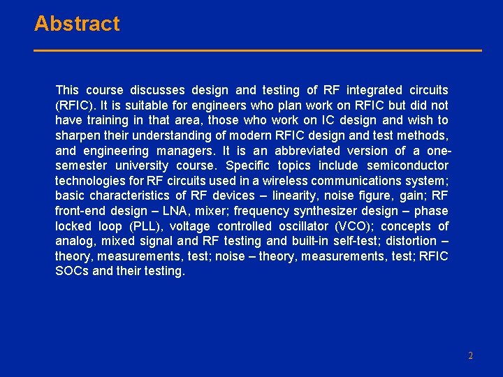
Abstract This course discusses design and testing of RF integrated circuits (RFIC). It is suitable for engineers who plan work on RFIC but did not have training in that area, those who work on IC design and wish to sharpen their understanding of modern RFIC design and test methods, and engineering managers. It is an abbreviated version of a onesemester university course. Specific topics include semiconductor technologies for RF circuits used in a wireless communications system; basic characteristics of RF devices – linearity, noise figure, gain; RF front-end design – LNA, mixer; frequency synthesizer design – phase locked loop (PLL), voltage controlled oscillator (VCO); concepts of analog, mixed signal and RF testing and built-in self-test; distortion – theory, measurements, test; noise – theory, measurements, test; RFIC SOCs and their testing. 2

Objectives q To acquire introductory knowledge about integrated circuits (IC) used in radio frequency (RF) communications systems. q To learn basic concept of design of RFIC. q To learn basic concepts of RFIC testing. 3

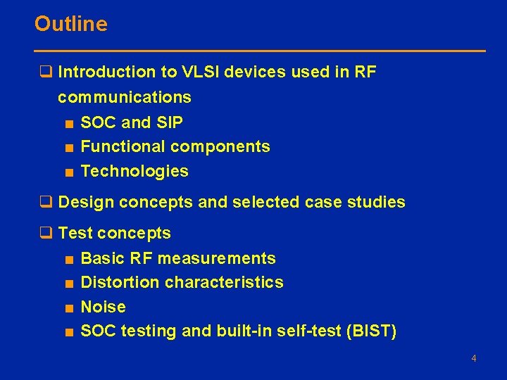
Outline q Introduction to VLSI devices used in RF communications ■ SOC and SIP ■ Functional components ■ Technologies q Design concepts and selected case studies q Test concepts ■ Basic RF measurements ■ Distortion characteristics ■ Noise ■ SOC testing and built-in self-test (BIST) 4

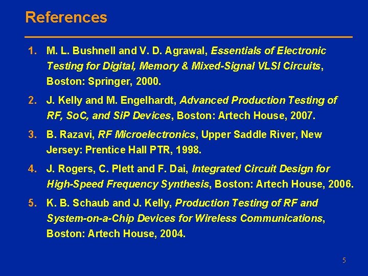
References 1. M. L. Bushnell and V. D. Agrawal, Essentials of Electronic Testing for Digital, Memory & Mixed-Signal VLSI Circuits, Boston: Springer, 2000. 2. J. Kelly and M. Engelhardt, Advanced Production Testing of RF, So. C, and Si. P Devices, Boston: Artech House, 2007. 3. B. Razavi, RF Microelectronics, Upper Saddle River, New Jersey: Prentice Hall PTR, 1998. 4. J. Rogers, C. Plett and F. Dai, Integrated Circuit Design for High-Speed Frequency Synthesis, Boston: Artech House, 2006. 5. K. B. Schaub and J. Kelly, Production Testing of RF and System-on-a-Chip Devices for Wireless Communications, Boston: Artech House, 2004. 5

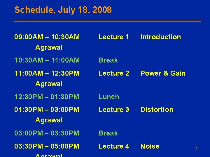
Schedule, July 18, 2008 09: 00 AM – 10: 30 AM Agrawal Lecture 1 10: 30 AM – 11: 00 AM Break 11: 00 AM – 12: 30 PM Agrawal Lecture 2 12: 30 PM – 01: 30 PM Lunch 01: 30 PM – 03: 00 PM Agrawal Lecture 3 03: 00 PM – 03: 30 PM Break 03: 30 PM – 05: 00 PM Lecture 4 Introduction Power & Gain Distortion Noise 6

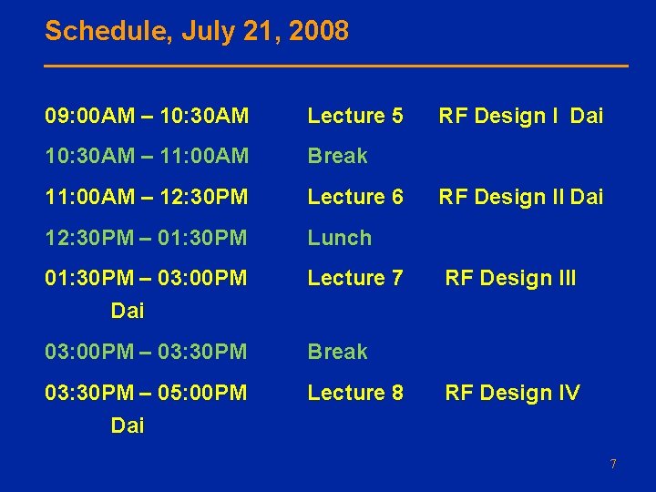
Schedule, July 21, 2008 09: 00 AM – 10: 30 AM Lecture 5 10: 30 AM – 11: 00 AM Break 11: 00 AM – 12: 30 PM Lecture 6 12: 30 PM – 01: 30 PM Lunch 01: 30 PM – 03: 00 PM Dai Lecture 7 03: 00 PM – 03: 30 PM Break 03: 30 PM – 05: 00 PM Dai Lecture 8 RF Design I Dai RF Design III RF Design IV 7

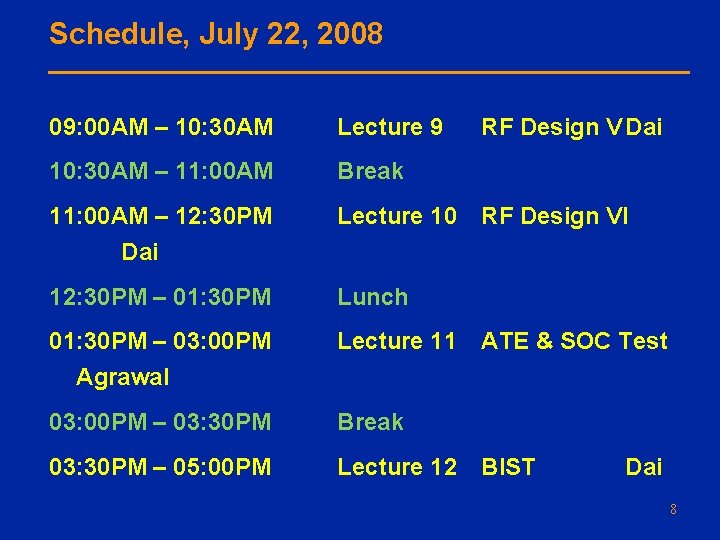
Schedule, July 22, 2008 09: 00 AM – 10: 30 AM Lecture 9 10: 30 AM – 11: 00 AM Break 11: 00 AM – 12: 30 PM Dai Lecture 10 12: 30 PM – 01: 30 PM Lunch 01: 30 PM – 03: 00 PM Agrawal Lecture 11 03: 00 PM – 03: 30 PM Break 03: 30 PM – 05: 00 PM Lecture 12 RF Design V Dai RF Design VI ATE & SOC Test BIST Dai 8

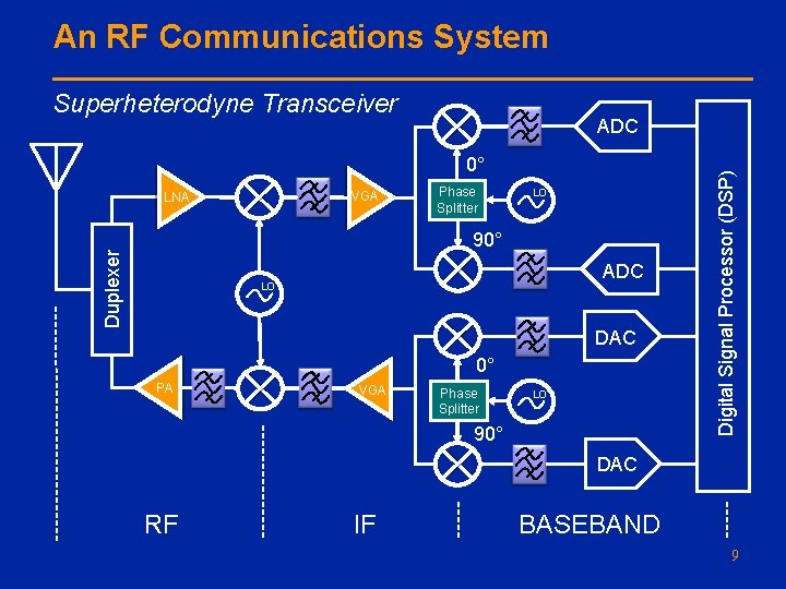
An RF Communications System Superheterodyne Transceiver 0° VGA LNA Phase Splitter LO Duplexer 90° ADC LO DAC 0° PA VGA Phase Splitter LO 90° Digital Signal Processor (DSP) ADC DAC RF IF BASEBAND 9

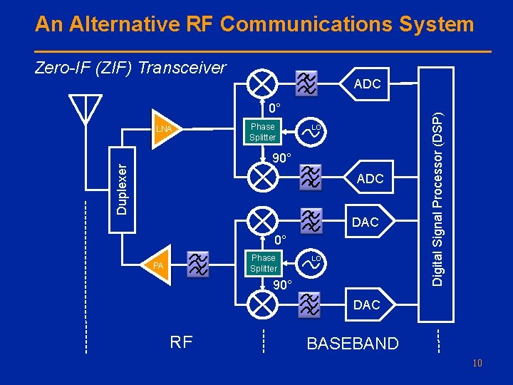
An Alternative RF Communications System Zero-IF (ZIF) Transceiver 0° LNA Phase Splitter LO Duplexer 90° ADC DAC 0° Phase Splitter PA LO 90° Digital Signal Processor (DSP) ADC DAC RF BASEBAND 10

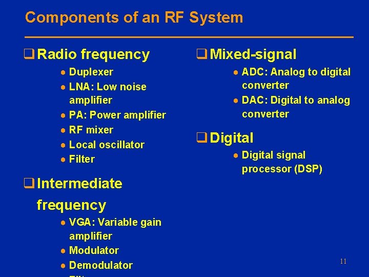
Components of an RF System q Radio frequency ● Duplexer ● LNA: Low noise amplifier ● PA: Power amplifier ● RF mixer ● Local oscillator ● Filter q Mixed-signal ● ADC: Analog to digital converter ● DAC: Digital to analog converter q Digital ● Digital signal processor (DSP) q Intermediate frequency ● VGA: Variable gain amplifier ● Modulator ● Demodulator 11

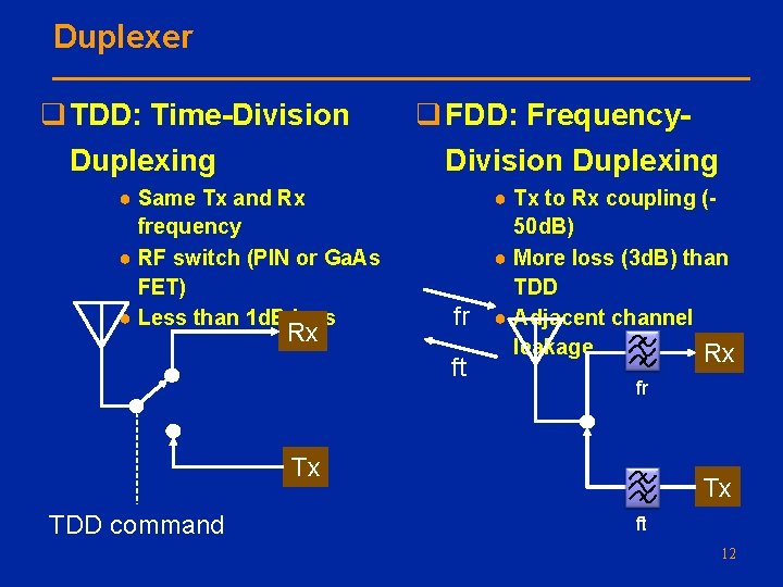
Duplexer q TDD: Time-Division Duplexing ● Same Tx and Rx frequency ● RF switch (PIN or Ga. As FET) ● Less than 1 d. B loss Rx q FDD: Frequency. Division Duplexing fr ft ● Tx to Rx coupling (50 d. B) ● More loss (3 d. B) than TDD ● Adjacent channel leakage Rx fr Tx TDD command Tx ft 12

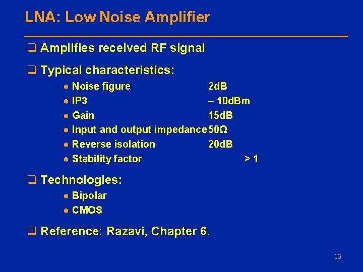
LNA: Low Noise Amplifier q Amplifies received RF signal q Typical characteristics: ● Noise figure 2 d. B ● IP 3 – 10 d. Bm ● Gain 15 d. B ● Input and output impedance 50Ω ● Reverse isolation 20 d. B ● Stability factor >1 q Technologies: ● Bipolar ● CMOS q Reference: Razavi, Chapter 6. 13

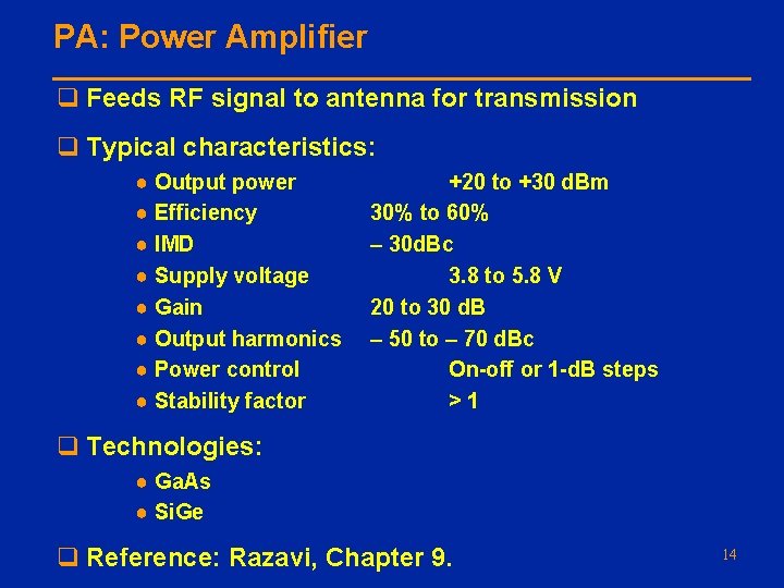
PA: Power Amplifier q Feeds RF signal to antenna for transmission q Typical characteristics: ● Output power ● Efficiency ● IMD ● Supply voltage ● Gain ● Output harmonics ● Power control ● Stability factor +20 to +30 d. Bm 30% to 60% – 30 d. Bc 3. 8 to 5. 8 V 20 to 30 d. B – 50 to – 70 d. Bc On-off or 1 -d. B steps >1 q Technologies: ● Ga. As ● Si. Ge q Reference: Razavi, Chapter 9. 14

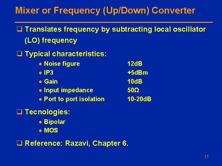
Mixer or Frequency (Up/Down) Converter q Translates frequency by subtracting local oscillator (LO) frequency q Typical characteristics: ● Noise figure ● IP 3 ● Gain ● Input impedance ● Port to port isolation 12 d. B +5 d. Bm 10 d. B 50Ω 10 -20 d. B q Tecnologies: ● Bipolar ● MOS q Reference: Razavi, Chapter 6. 15

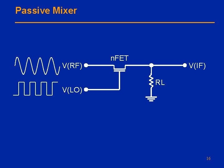
Passive Mixer V(RF) V(LO) n. FET V(IF) RL 16

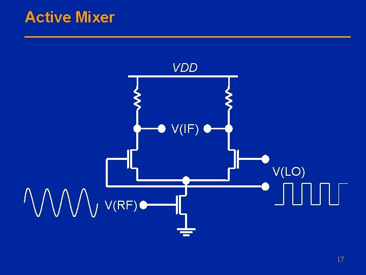
Active Mixer VDD V(IF) V(LO) V(RF) 17

LO: Local Oscillators q Provide signal to mixer for down conversion or upconversion. q Implementations: ● Tuned feedback amplifier ● Ring oscillator ● Phase-locked loop (PLL) ● Direct digital synthesizer (DDS) 18

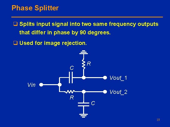
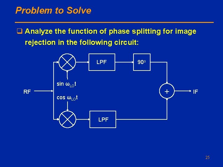
Phase Splitter q Splits input signal into two same frequency outputs that differ in phase by 90 degrees. q Used for image rejection. C R Vout_1 Vin R Vout_2 C 19

SOC: System-on-a-Chip q All components of a system are implemented on the same VLSI chip. q Requires same technology (usually CMOS) used for all components. q Components not implemented on present-day SOC: ● Antenna ● Power amplifier (PA) 20

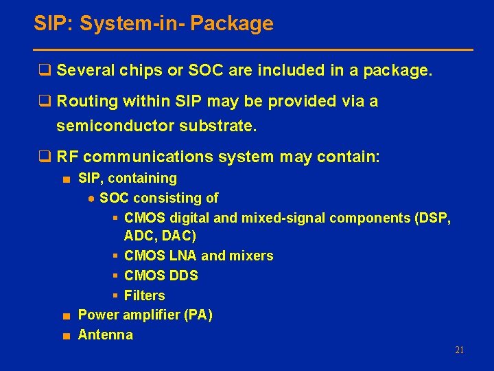
SIP: System-in- Package q Several chips or SOC are included in a package. q Routing within SIP may be provided via a semiconductor substrate. q RF communications system may contain: ■ SIP, containing ● SOC consisting of § CMOS digital and mixed-signal components (DSP, ADC, DAC) § CMOS LNA and mixers § CMOS DDS § Filters ■ Power amplifier (PA) ■ Antenna 21

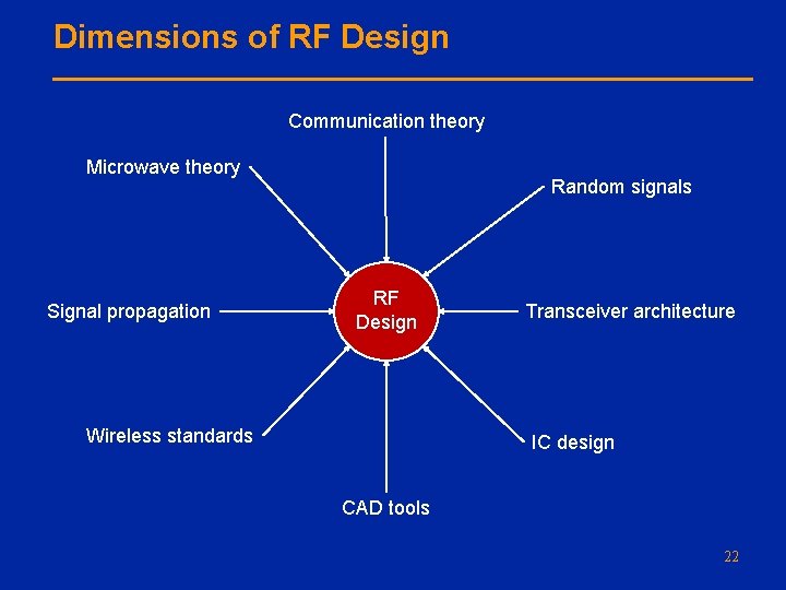
Dimensions of RF Design Communication theory Microwave theory Signal propagation Random signals RF Design Wireless standards Transceiver architecture IC design CAD tools 22

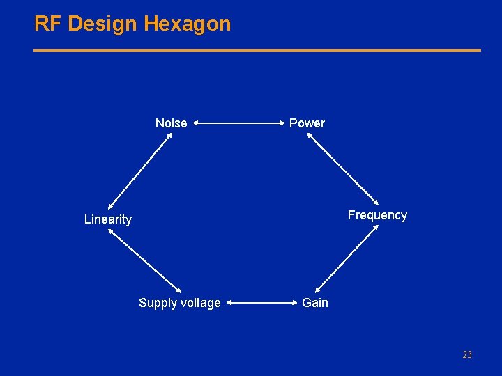
RF Design Hexagon Noise Power Frequency Linearity Supply voltage Gain 23

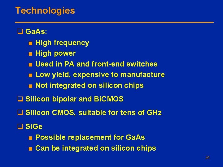
Technologies q Ga. As: ■ High frequency ■ High power ■ Used in PA and front-end switches ■ Low yield, expensive to manufacture ■ Not integrated on silicon chips q Silicon bipolar and Bi. CMOS q Silicon CMOS, suitable for tens of GHz q Si. Ge ■ Possible replacement for Ga. As ■ Can be integrated on silicon chips 24

Problem to Solve q Analyze the function of phase splitting for image rejection in the following circuit: LPF sin ωLOt RF 90 o + cos ωLOt IF LPF 25