Report on Superconducting RF Materials Workshop Lance Cooley
- Slides: 27
Report on Superconducting RF Materials Workshop Lance Cooley SRF Materials Group Leader Fermilab f SRF workshop report, HEP 6/15/07
Workshop overview http: //tdserver 1. fnal. gov/project/workshops/RF_Materials/ • May 23 -24, 2007, Fermilab • Organized by Helen Edwards, Genfa Wu, and Claire Antoine • About 50 participants • Purpose: encourage participation in SRF science by academia, industry, and basic science labs in a LTSWlike format • Focused discussions organized by program committee toward topics of basic interest to SRF science, while in the context of real cavities with real deliverables f SRF workshop report, HEP 6/15/07
A brief history • Regional workshops 2005 and 2006 organized by Pierre Bauer and Claire Antoine (Midwest SRF Collaboration): FNAL, UW, NU, MSU • Materials workshop at FNAL 2001, DESY 2003 mostly Cornell – JLAB – DESY – KEK • 13 th annual International Workshop on RF Superconductivity, Beijing, October 2007 • Intention: continue national workshop in the spirit of LTSW annually or semi-annually f SRF workshop report, HEP 6/15/07
Charge from Claire Antoine • • Understand basic issues Evolve beyond niobium’s limits; open up new frontiers Understand physics and materials science Bring to bear surface science coordinated with characterization of real cavities • Build interactions, form coordinated research activities, promote interdisciplinary studies • Extend SRF materials community to basic science • Expand SRF materials community to academia and industry f SRF workshop report, HEP 6/15/07
Workshop topics • • • Fundamentals of RF superconductivity Materials properties and surface characterizations New materials Innovative processing of materials Production of niobium f SRF workshop report, HEP 6/15/07
Main Findings • A new era may be emerging where internal surfaces of RF cavities are engineered by design. – – • Exciting new tools make it possible to search out problem areas and perform materials science Conformal multilayers Protective coatings Roughness removal Re-plating Nb – RF microscope – Scanned laser microscope – Orientation imaging microscopy • Gurevich theory to break niobium monopoly can now be tested in real cavity forms • An analog of the “short sample test” is missing f SRF workshop report, HEP 6/15/07 – LANL cavity – U Md resonator
Main Findings, cont. • Progress toward understanding inter-relationships between surface structure, surface chemistry, and Nb cavity performance – Oxygen and oxides – Tantalum: relax spec? – QA and tracking processing history • Alternatives to HF etching exist – Ion cluster bombardment – Plasma etching – Single crystals (already smooth) f SRF workshop report, HEP 6/15/07 • Much work is bootstrapped or supported by seed funds. Some efforts are on a precipice – need support now. • New talent is being uncovered!
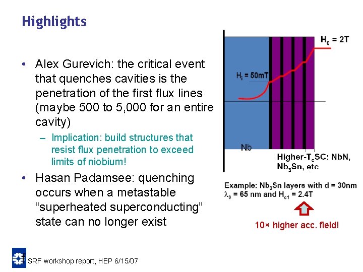
Highlights • Alex Gurevich: the critical event that quenches cavities is the penetration of the first flux lines (maybe 500 to 5, 000 for an entire cavity) – Implication: build structures that resist flux penetration to exceed limits of niobium! • Hasan Padamsee: quenching occurs when a metastable “superheated superconducting” state can no longer exist f SRF workshop report, HEP 6/15/07 10× higher acc. field!
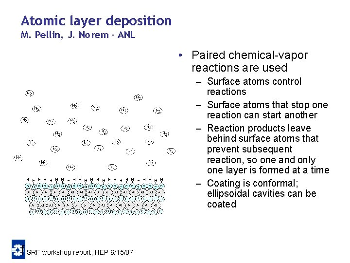
Atomic layer deposition M. Pellin, J. Norem - ANL • Paired chemical-vapor reactions are used – Surface atoms control reactions – Surface atoms that stop one reaction can start another – Reaction products leave behind surface atoms that prevent subsequent reaction, so one and only one layer is formed at a time – Coating is conformal; ellipsoidal cavities can be coated f SRF workshop report, HEP 6/15/07
Highlights • Tantalum content from 200 to 1300 wt. ppm does not seem to produce a performance change when cavities are operating at ~25 MV/m. – Therefore, should we relax the spec to reduce cost? • Tantalum content does produce a small dropoff in performance, about 10%, for ~35 MV/m cavities. – No Ta-rich cavity exceeded 33 MV/m f SRF workshop report, HEP 6/15/07
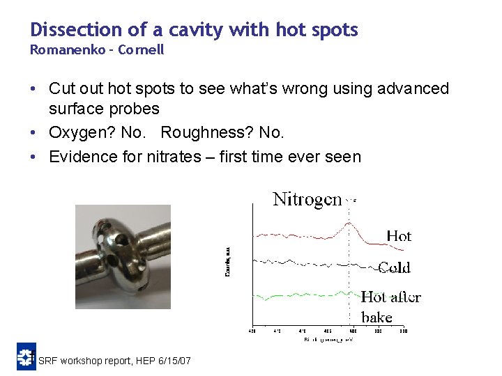
Dissection of a cavity with hot spots Romanenko - Cornell • Cut out hot spots to see what’s wrong using advanced surface probes • Oxygen? No. Roughness? No. • Evidence for nitrates – first time ever seen f SRF workshop report, HEP 6/15/07
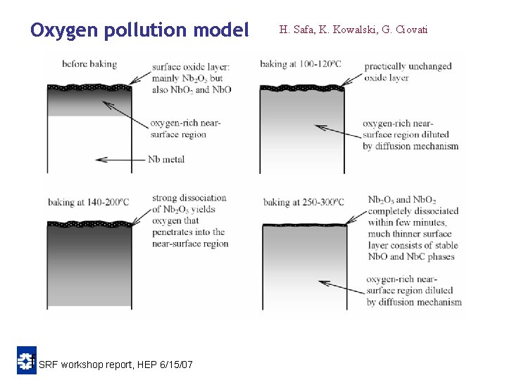
Oxygen pollution model f SRF workshop report, HEP 6/15/07 H. Safa, K. Kowalski, G. Ciovati
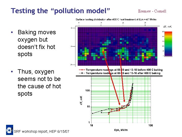
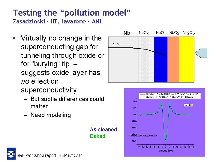
Testing the “pollution model” • Baking moves oxygen but doesn’t fix hot spots • Thus, oxygen seems not to be the cause of hot spots f SRF workshop report, HEP 6/15/07 Eremev - Cornell
Testing the “pollution model” Zasadzinski – IIT, Iavarone - ANL • Virtually no change in the superconducting gap for tunneling through oxide or for “burying” tip – suggests oxide layer has no effect on superconductivity! – But subtle differences could matter – Need modeling As-cleaned Baked f SRF workshop report, HEP 6/15/07
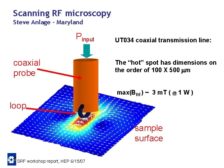
Scanning RF microscopy Steve Anlage - Maryland Pinput coaxial probe UT 034 coaxial transmission line: The “hot” spot has dimensions on the order of 100 X 500 mm max(BRF) ~ 3 m. T ( @ 1 W ) loop sample surface f SRF workshop report, HEP 6/15/07
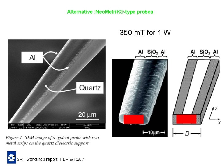
Alternative : Neo. Metri. K®-type probes 350 m. T for 1 W f SRF workshop report, HEP 6/15/07
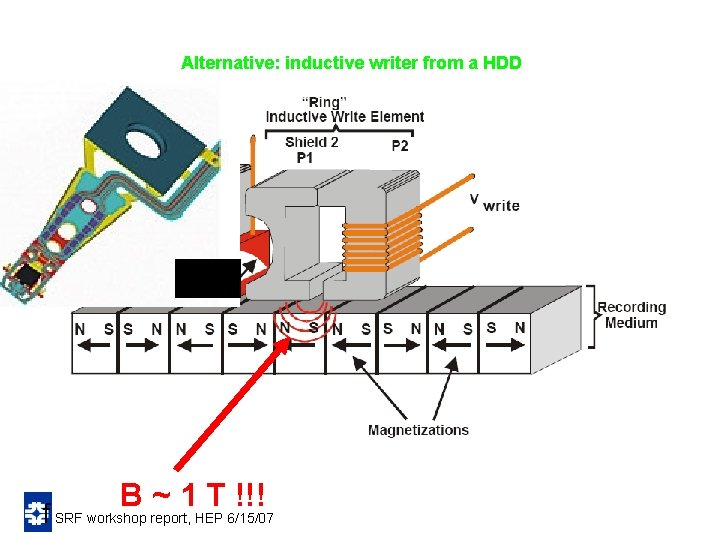
Alternative: inductive writer from a HDD B ~ 1 T !!! f SRF workshop report, HEP 6/15/07
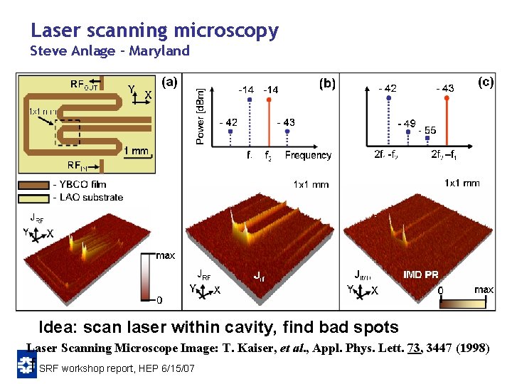
Laser scanning microscopy Steve Anlage - Maryland Idea: scan laser within cavity, find bad spots Laser Scanning Microscope Image: T. Kaiser, et al. , Appl. Phys. Lett. 73, 3447 (1998) f SRF workshop report, HEP 6/15/07
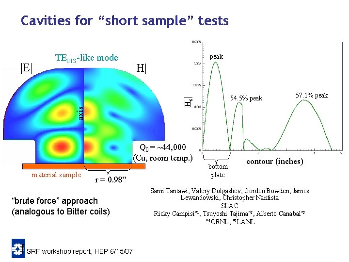
Cavities for “short sample” tests peak |H| 54. 5% peak |Hs| axis |E| TE 013 -like mode Q 0 = ~44, 000 (Cu, room temp. ) material sample r = 0. 98” “brute force” approach (analogous to Bitter coils) f SRF workshop report, HEP 6/15/07 bottom plate 57. 1% peak contour (inches) Sami Tantawi, Valery Dolgashev, Gordon Bowden, James Lewandowski, Christopher Nantista SLAC *1 Ricky Campisi , Tsuyoshi Tajima*2, Alberto Canabal*2 *1 ORNL, *2 LANL
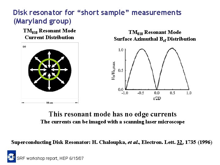
Disk resonator for “short sample” measurements (Maryland group) TM 010 Resonant Mode Current Distribution TM 010 Resonant Mode Surface Azimuthal Brf Distribution This resonant mode has no edge currents The currents can be imaged with a scanning laser microscope Superconducting Disk Resonator: H. Chaloupka, et al. , Electron. Lett. 32, 1735 (1996) f SRF workshop report, HEP 6/15/07
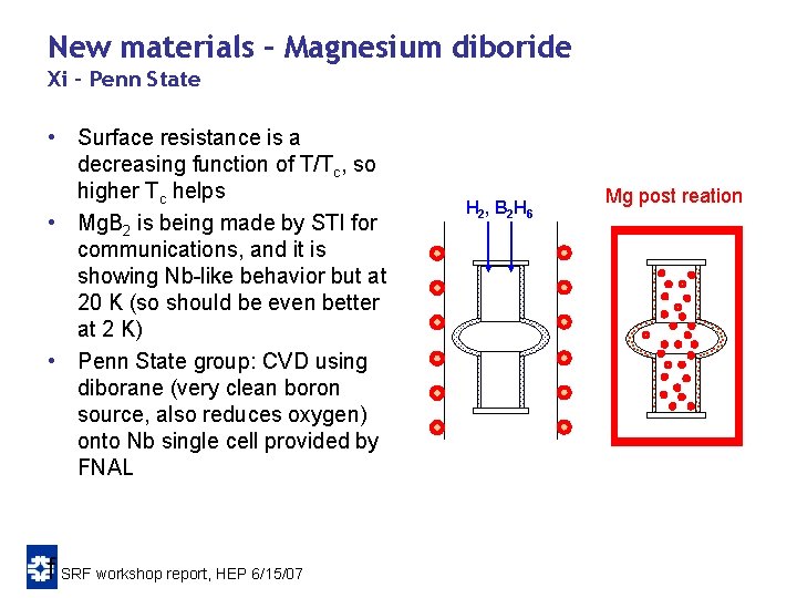
New materials – Magnesium diboride Xi – Penn State • Surface resistance is a decreasing function of T/Tc, so higher Tc helps • Mg. B 2 is being made by STI for communications, and it is showing Nb-like behavior but at 20 K (so should be even better at 2 K) • Penn State group: CVD using diborane (very clean boron source, also reduces oxygen) onto Nb single cell provided by FNAL f SRF workshop report, HEP 6/15/07 H 2 , B 2 H 6 Mg post reation
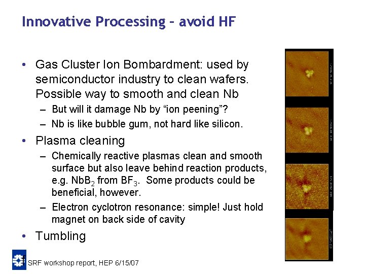
Innovative Processing – avoid HF • Gas Cluster Ion Bombardment: used by semiconductor industry to clean wafers. Possible way to smooth and clean Nb – But will it damage Nb by “ion peening”? – Nb is like bubble gum, not hard like silicon. • Plasma cleaning – Chemically reactive plasmas clean and smooth surface but also leave behind reaction products, e. g. Nb. B 2 from BF 3. Some products could be beneficial, however. – Electron cyclotron resonance: simple! Just hold magnet on back side of cavity • Tumbling f SRF workshop report, HEP 6/15/07
Niobium Processing • Grain size issues – Small grains: good formability and low roughness upon etching, but can trap impurities in boundaries – Large grains: grain interiors are smooth, but big steps at boundaries (roughness) and tolerances difficult to hold – Single crystals: very smooth, very well behaved mechanically, but expensive. Engineering is just beginning. Do properties depend on crystallographic orientation? • Specifications – Specs may not be internally consistent and may force vendor to treat the surface (the “kiss pass”). Delivered sheets are thus composites. – Reduce Ta? f SRF workshop report, HEP 6/15/07
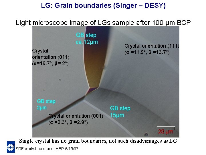
LG: Grain boundaries (Singer – DESY) Light microscope image of LGs sample after 100 µm BCP GB step ca. 12µm Crystal orientation (011) (α=19. 7°, β= 2°) GB step 2µm Crystal orientation (001) (α =2. 3°, β =2. 9°) Crystal orientation (111) (α =11. 9°, β =13. 7°) GB step 15µm Single crystal has no grain boundaries, not such disadvantages as LG f SRF workshop report, HEP 6/15/07
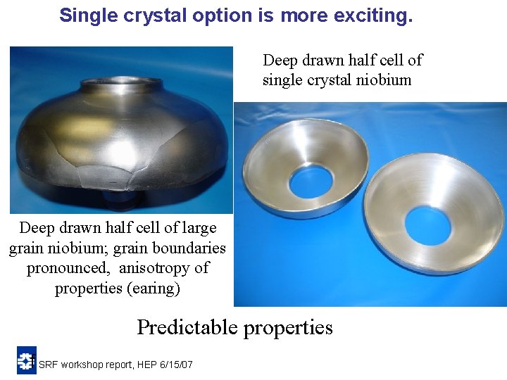
Single crystal option is more exciting. Deep drawn half cell of single crystal niobium Deep drawn half cell of large grain niobium; grain boundaries pronounced, anisotropy of properties (earing) Predictable properties f SRF workshop report, HEP 6/15/07
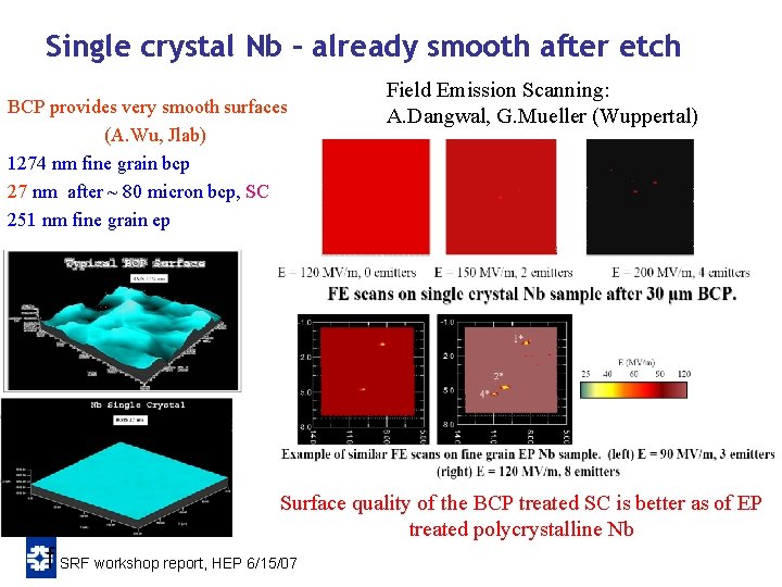
Single crystal Nb – already smooth after etch BCP provides very smooth surfaces (A. Wu, Jlab) 1274 nm fine grain bcp 27 nm after ~ 80 micron bcp, SC 251 nm fine grain ep Field Emission Scanning: A. Dangwal, G. Mueller (Wuppertal) Surface quality of the BCP treated SC is better as of EP treated polycrystalline Nb f SRF workshop report, HEP 6/15/07
Concluding Remarks for HEP • There are many pathways for breakthroughs! Two genres: Validate/confirm/challenge ILC processes, and Excellence in SRF science • Potential knowledge gain can be very rapid with time over next 3 -5 years IF the interested basic scientists can be supported. • More and more industry players – a good thing. Now we need to tune SBIR language and continue to build relationships with end users. • FNAL (me) will continue to coordinate and build national effort (it’s in the job description). f SRF workshop report, HEP 6/15/07