Radiation Damage Tests at 1 GRad Dose on

- Slides: 31

Radiation Damage Tests at 1 GRad Dose on 65 nm CMOS transistors Marlon Barbero – CPPM Grezgorz Deptuch –FNAL The RD 53 collaboration

Plan • • • RD 53 & CERN upgrades. Effect of radiation on CMOS. Few results on test transistors. Few results on ICs and blocks. Conclusion. Rad Effects in 65 nm, M. Barbero / G. Deptuch, Mai 23 rd 2014 2

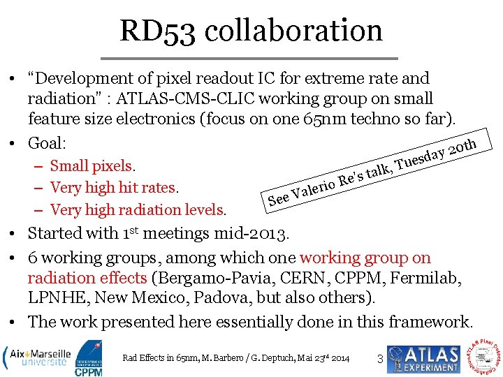
RD 53 collaboration • “Development of pixel readout IC for extreme rate and radiation” : ATLAS-CMS-CLIC working group on small feature size electronics (focus on one 65 nm techno so far). • Goal: 20 th – Small pixels. – Very high hit rates. – Very high radiation levels. ay d s e , Tu lk ’s ta e R io ler a V See • Started with 1 st meetings mid-2013. • 6 working groups, among which one working group on radiation effects (Bergamo-Pavia, CERN, CPPM, Fermilab, LPNHE, New Mexico, Padova, but also others). • The work presented here essentially done in this framework. Rad Effects in 65 nm, M. Barbero / G. Deptuch, Mai 23 rd 2014 3

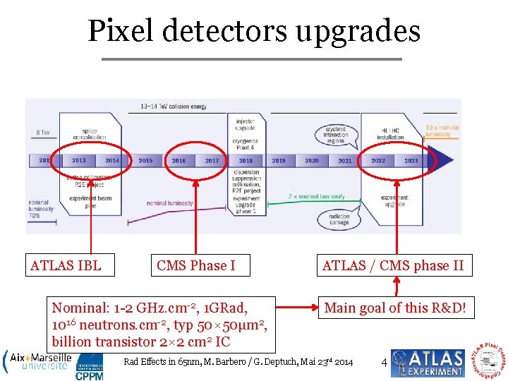
Pixel detectors upgrades ATLAS IBL CMS Phase I Nominal: 1 -2 GHz. cm-2, 1 GRad, 1016 neutrons. cm-2, typ 50× 50μm 2, billion transistor 2× 2 cm 2 IC ATLAS / CMS phase II Main goal of this R&D! Rad Effects in 65 nm, M. Barbero / G. Deptuch, Mai 23 rd 2014 4

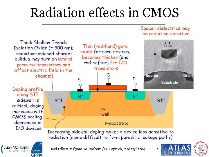
Radiation effects in CMOS Rad Effects in 65 nm, M. Barbero / G. Deptuch, Mai 23 rd 2014 5

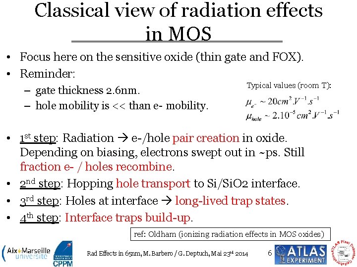
Classical view of radiation effects in MOS • Focus here on the sensitive oxide (thin gate and FOX). • Reminder: – gate thickness 2. 6 nm. – hole mobility is << than e- mobility. Typical values (room T): • 1 st step: Radiation e-/hole pair creation in oxide. Depending on biasing, electrons swept out in ~ps. Still fraction e- / holes recombine. • 2 nd step: Hopping hole transport to Si/Si. O 2 interface. • 3 rd step: Holes at interface long-lived trap states. • 4 th step: Interface traps build-up. ref: Oldham (ionizing radiation effects in MOS oxides) Rad Effects in 65 nm, M. Barbero / G. Deptuch, Mai 23 rd 2014 6

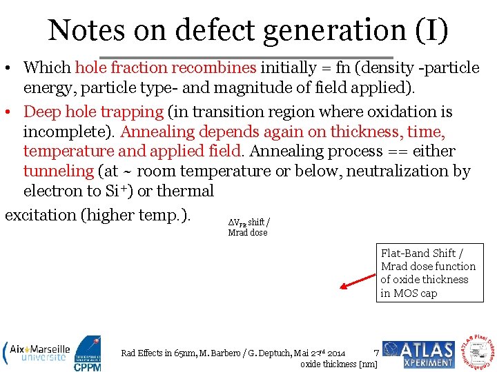
Notes on defect generation (I) • Which hole fraction recombines initially = fn (density -particle energy, particle type- and magnitude of field applied). • Deep hole trapping (in transition region where oxidation is incomplete). Annealing depends again on thickness, time, temperature and applied field. Annealing process == either tunneling (at ~ room temperature or below, neutralization by electron to Si+) or thermal excitation (higher temp. ). ΔV shift / FB Mrad dose Flat-Band Shift / Mrad dose function of oxide thickness in MOS cap Rad Effects in 65 nm, M. Barbero / G. Deptuch, Mai 23 rd 2014 7 oxide thickness [nm]

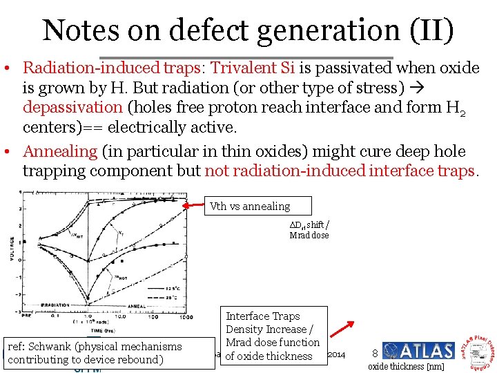
Notes on defect generation (II) • Radiation-induced traps: Trivalent Si is passivated when oxide is grown by H. But radiation (or other type of stress) depassivation (holes free proton reach interface and form H 2 centers)== electrically active. • Annealing (in particular in thin oxides) might cure deep hole trapping component but not radiation-induced interface traps. Vth vs annealing ΔDit shift / Mrad dose Interface Traps Density Increase / Mrad dose function ref: Schwank (physical mechanisms Rad Effects in 65 nm, M. Barbero / G. Deptuch, Mai 23 rd 2014 of oxide thickness contributing to device rebound) 8 oxide thickness [nm]

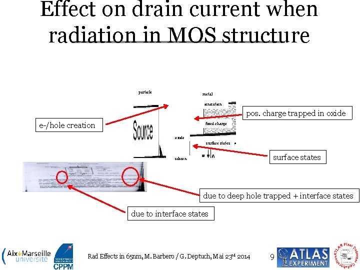
Effect on drain current when radiation in MOS structure particle metal ionization pos. charge trapped in oxide e-/hole creation fixed charge oxide surface states silicon due to deep hole trapped + interface states due to interface states Rad Effects in 65 nm, M. Barbero / G. Deptuch, Mai 23 rd 2014 9

Radiation Induced Narrow Channel Effect -RINCE- • Trapping in STI of rad-induced positive charges opens inversion channel / parasitic transistor. • Strong dependence on width of transistor: for narrow transistors, influence of parasitic channels strong competitor to main channel. ref: Faccio (radiation induced edge effect in deep submicron CMOS transistors) Rad Effects in 65 nm, M. Barbero / G. Deptuch, Mai 23 rd 2014 10

A word from the past • CMS / ATLAS current Front-End: – 250 nm technology. – ~50 MRad. – Use of enclosed layout + guard rings. Custom libraries!!! If so, safe! • ATLAS IBL (FE-I 4): – 130 nm. – ~250 MRad. – Minimum W imposed. If so, safe! Rad Effects in 65 nm, M. Barbero / G. Deptuch, Mai 23 rd 2014 11

Effects on test transistors: results Rad Effects in 65 nm, M. Barbero / G. Deptuch, Mai 23 rd 2014 12

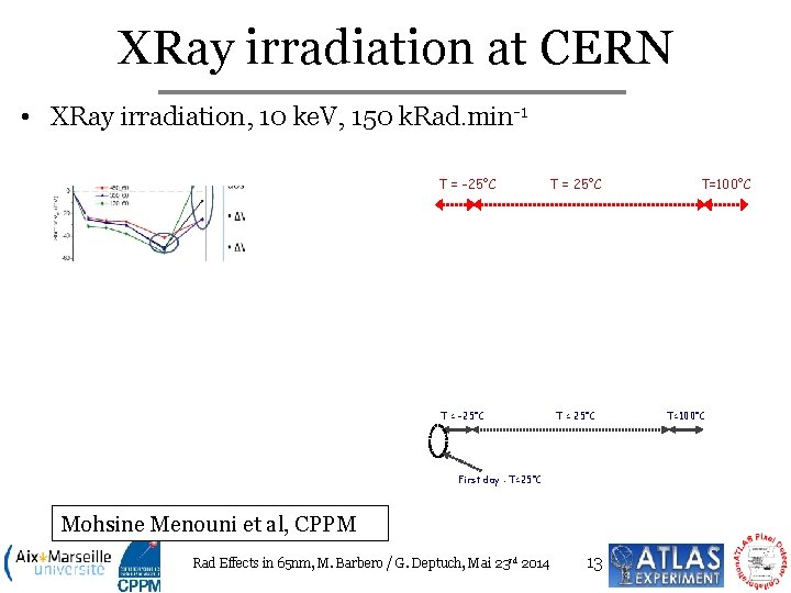
XRay irradiation at CERN • XRay irradiation, 10 ke. V, 150 k. Rad. min-1 T = -25°C T = 25°C First day : T=25°C Mohsine Menouni et al, CPPM Rad Effects in 65 nm, M. Barbero / G. Deptuch, Mai 23 rd 2014 13 T=100°C

NMOS threshold shift • A little decrease of the threshold for low dose level – -20 m. V shift for the minimum width device • For levels of dose > 200 Mrad, the absolute value of Vth increases – At 1000 Mrad, the Vth shift is between 150 m. V to 320 m. V depending on the device width (maximum for 240 nm/60 nm) • The Vth recovery at room temperature is very slow – Except at the beginning of annealing period and only for the narrowest devices (W=120 nm and W=240 nm) • High Temperature annealing (100 °C for 7 days) : – The Vth recovery is accelerated – The global Vth shift is < 200 m. V – Reverse annealing behavior for the device with W=120 nm (Vth first decreases and increases after) Rad Effects in 65 nm, M. Barbero / G. Deptuch, Mai 23 rd 2014 14

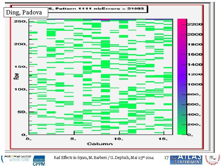
Proton irradiation • 3 Me. V proton -1016 neq. cm-2 -, 3. 6 - 36 MRad. min-1 , 15 Lili Ding et al, Padova. Rad Effects in 65 nm, M. Barbero / G. Deptuch, Mai 23 rd 2014

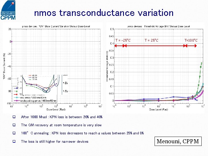
nmos transconductance variation T = -25°C q After 1000 Mrad : KPN loss is between 20% and 40% q The GM recovery at room temperature is very slow q 100°C annealing : KPN loss decreases to reach a values between 25% and 8% q The loss is still higher for narrower devices T = 25°C T=100°C Menouni, CPPM

Ding, Padova Rad Effects in 65 nm, M. Barbero / G. Deptuch, Mai 23 rd 2014 17

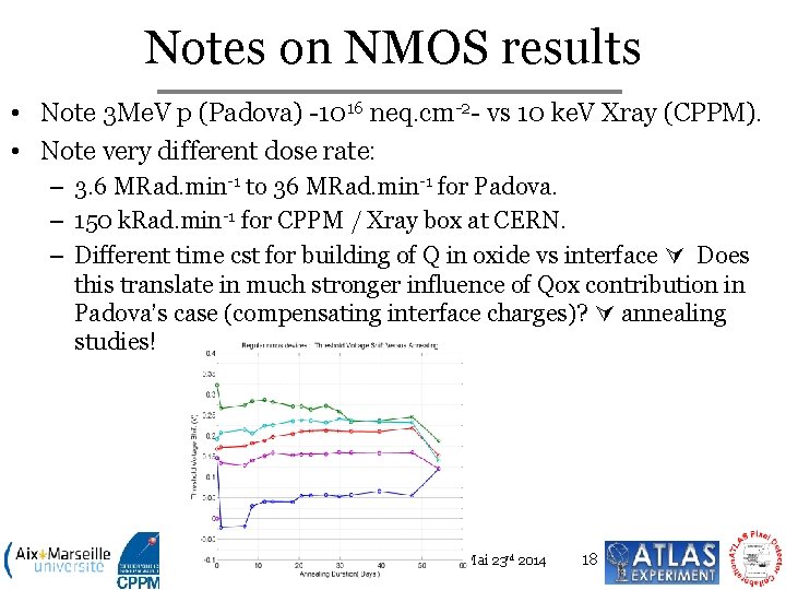
Notes on NMOS results • Note 3 Me. V p (Padova) -1016 neq. cm-2 - vs 10 ke. V Xray (CPPM). • Note very different dose rate: – 3. 6 MRad. min-1 to 36 MRad. min-1 for Padova. – 150 k. Rad. min-1 for CPPM / Xray box at CERN. – Different time cst for building of Q in oxide vs interface Does this translate in much stronger influence of Qox contribution in Padova’s case (compensating interface charges)? annealing studies! Rad Effects in 65 nm, M. Barbero / G. Deptuch, Mai 23 rd 2014 18

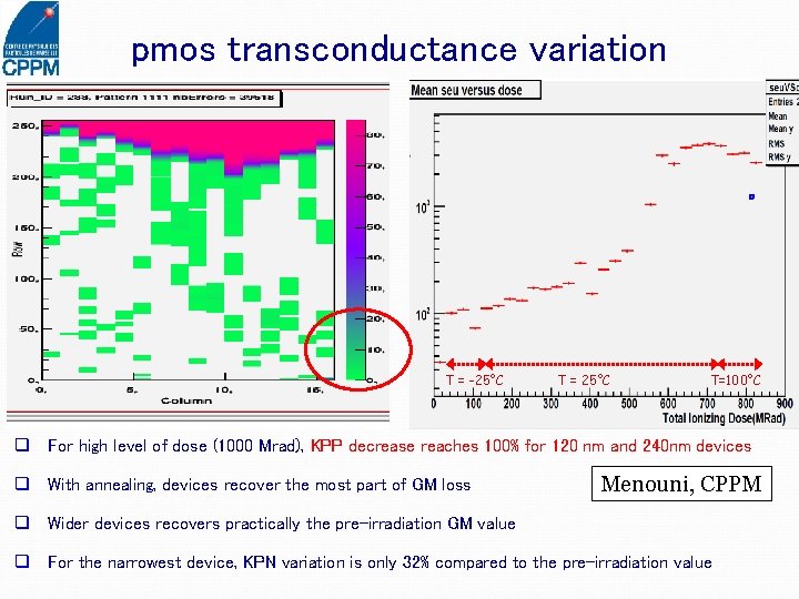
pmos transconductance variation T = -25°C T = 25°C T=100°C q For high level of dose (1000 Mrad), KPP decrease reaches 100% for 120 nm and 240 nm devices q With annealing, devices recover the most part of GM loss Menouni, CPPM q Wider devices recovers practically the pre-irradiation GM value q For the narrowest device, KPN variation is only 32% compared to the pre-irradiation value

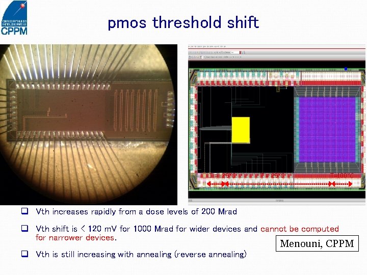
pmos threshold shift T = -25°C T = 25°C T=100°C q Vth increases rapidly from a dose levels of 200 Mrad q Vth shift is < 120 m. V for 1000 Mrad for wider devices and cannot be computed for narrower devices. q Vth is still increasing with annealing (reverse annealing) Menouni, CPPM

Effects on IC and blocks: results Rad Effects in 65 nm, M. Barbero / G. Deptuch, Mai 23 rd 2014 21

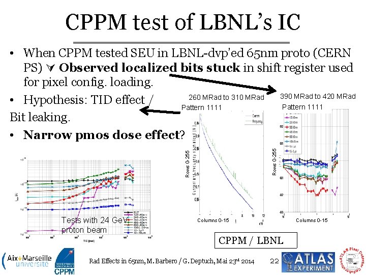
CPPM test of LBNL’s IC Rows 0 -255 • When CPPM tested SEU in LBNL-dvp’ed 65 nm proto (CERN PS) Observed localized bits stuck in shift register used for pixel config. loading. 390 MRad to 420 MRad 260 MRad to 310 MRad • Hypothesis: TID effect / Pattern 1111 Bit leaking. • Narrow pmos dose effect? Tests with 24 Ge. V proton beam Columns 0 -15 CPPM / LBNL Rad Effects in 65 nm, M. Barbero / G. Deptuch, Mai 23 rd 2014 22

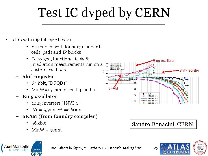
Test IC dvped by CERN • chip with digital logic blocks • Assembled with foundry standard cells, pads and IP blocks • Packaged, functional tests & irradiation measurements run on a custom test board – Shift-register • 64 kbit, “DFQD 1” • Min. W=150 nm for both p and n – Ring oscillator • 1025 inverters “INVD 0” • Wn=195 nm, Wp=260 nm – SRAM (from foundry compiler) • 56 kbit • Min. W = 90 nm Ring oscillator Shift-register SRAM Sandro Bonacini, CERN Rad Effects in 65 nm, M. Barbero / G. Deptuch, Mai 23 rd 2014 23

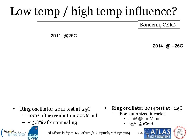
Low temp / high temp influence? Bonacini, CERN 2011, @25 C 2014, @ – 25 C • Ring oscillator 2011 test at 25 C – -22% after irradiation 200 Mrad – -13. 8% after annealing • Ring oscillator 2014 test at – 25 C – For same sized inverter: • -10% @200 Mrad • -35% @1 Grad Rad Effects in 65 nm, M. Barbero / G. Deptuch, Mai 23 rd 2014 24

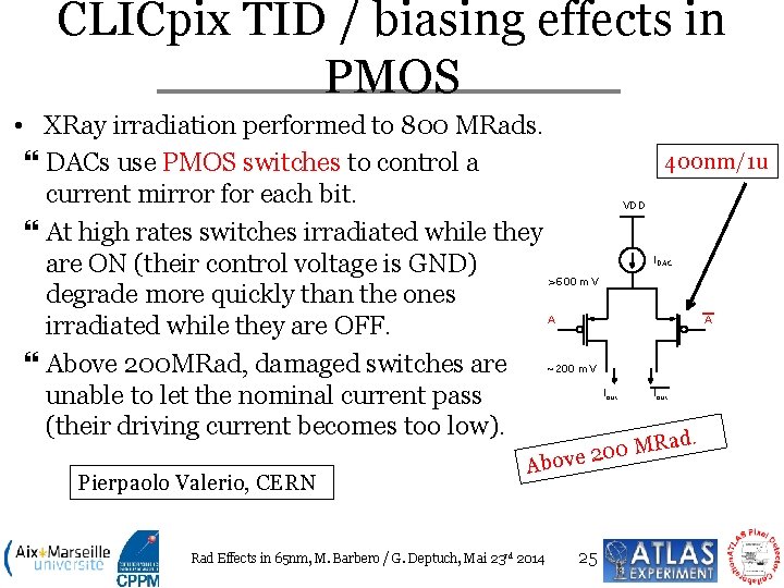
CLICpix TID / biasing effects in PMOS • XRay irradiation performed to 800 MRads. DACs use PMOS switches to control a current mirror for each bit. At high rates switches irradiated while they are ON (their control voltage is GND) >600 m. V degrade more quickly than the ones A irradiated while they are OFF. Above 200 MRad, damaged switches are ~200 m. V I unable to let the nominal current pass (their driving current becomes too low). out 400 nm/1 u VDD IDAC A Iout d. a R M e 200 Pierpaolo Valerio, CERN Abov Rad Effects in 65 nm, M. Barbero / G. Deptuch, Mai 23 rd 2014 25

BUT… All I/O interfaces and digital structures did not show any significant degradation during irradiation, even after the analog front-end stopped working The chips regained some functionality after two week of annealing at room temperature (the total power consuption went back to pre-rad value). Analog performances of the measured chip were found to be considerably degraded. The measurement was performed at a dose rate of ~150 krad/minute (~75 krad/minute for the first 10 Mrads). The high dose rate could have an effect on the radiation damage and needs to be explored Pierpaolo Valerio, CERN Rad Effects in 65 nm, M. Barbero / G. Deptuch, Mai 23 rd 2014 26

Summary • • Unexplored territory in terms of process and radiation level. Studies done so far on one 65 nm technology mainly. Gate effects / STI effects not clearly disentangled so-far. NMOS: shift of Vth, drive capability loss… steep increase above 200 MRads. Still, provided one could handle degradation, depending on application, hint that devices might be operated to close to ~1 GRad TID down to small W. • PMOS: Strong drive loss, narrowest devices completely off above few 100 MRads. Indication that narrowest devices will not work at close to 1 GRad. • Effects seeing in test IC too. Rad Effects in 65 nm, M. Barbero / G. Deptuch, Mai 23 rd 2014 27

Outlook • Still studies too preliminary and more work to be done in wellcontrolled conditions: Biasing for PMOS? Influence of temperature? Annealing scenario? • Then: Other damages type (Xray / neutron/ proton … investigate if DD becomes an issue). LDR vs HDR? • Relation to other stresses: NBTI, HCI… • If it is confirmed that damage is unacceptable, 2 ways out: • Other technologies (work starts on that topic, with limited momentum so far). • Rules for design to be established to allow intermediate dose level to be reached and replacement strategy. • Still to come later: SEE studies / Statistical spread after irrad / Modelling after irrad /etc… Rad Effects in 65 nm, M. Barbero / G. Deptuch, Mai 23 rd 2014 28

BACKUP • BACKUP Rad Effects in 65 nm, M. Barbero / G. Deptuch, Mai 23 rd 2014 29

Core NMOS radiation performance Leakage current Threshold voltage shift n n Up to ~20 m. V shift for 200 Mrad q Some rebound effect visible for narrow devices q in 130 nm: was 150 m. V n n At high doses Vth shift is positive for wide devices, negative for narrow devices q n STI edge oxide traps considerable charge (RINCE) Subtreshold slope does not change significantly n Less than 10× increase in leakage for wide devices (W > 360 nm) Narrow devices have up to 2. 5 orders of magnitude increase In 130 nm: q q q All devices are peaking at ~100 n. A Narrow devices increase leakage by 3 orders of magnitude Ileak is ~1 n. A @136 Mrad Sandro Bonacini - PH/ESE - sandro. bonacini@cern. ch 30

Core PMOS: Vth shift and gm loss n PMOS Vth shift limited to 60 m. V q q q n gm, max trapped charge and interface states sum up More evident for narrow devices Less than 10 m. V for transistors with W>1 um Compared to other technologies q Better performance than 130 nm n n q n had up to 90 m. V @136 Mrad 30 m. V for wide devices In a 90 nm tech we observed a similar effect: 70 m. V @ 200 Mrad Radiation kills maximum gm, max (strong inversion) q . . . but not gm in weak inversion region Sandro Bonacini - PH/ESE - sandro. bonacini@cern. ch 31