QIE 10 11 Readout Chip Development T Zimmerman
![Overview of multi-decade QIE development • • The QIE [Charge (Q) Integrator and Encoder] Overview of multi-decade QIE development • • The QIE [Charge (Q) Integrator and Encoder]](https://slidetodoc.com/presentation_image_h/9314f730c7ba8b1c6769cf7941761933/image-2.jpg)
- Slides: 22

QIE 10 -11 Readout Chip Development T. Zimmerman Fermi National Accelerator Laboratory FEE 2014 Argonne National Laboratory May 20, 2014
![Overview of multidecade QIE development The QIE Charge Q Integrator and Encoder Overview of multi-decade QIE development • • The QIE [Charge (Q) Integrator and Encoder]](https://slidetodoc.com/presentation_image_h/9314f730c7ba8b1c6769cf7941761933/image-2.jpg)
Overview of multi-decade QIE development • • The QIE [Charge (Q) Integrator and Encoder] is a custom ASIC designed to digitize wide dynamic range charge signals from photo-detectors (PMTs, Si. PMs), with approximately constant resolution and no deadtime A short history: – 1989: Originally conceived by Bill Foster for SDC @ SSC – 1995: 1 st fully-functional chip designed by Tom Zimmerman for the KTe. V experiment @ FNAL (QIE 5) • 2 mm Orbit “Bi-CMOS”, 3000 ch. – 1996: Front-end for calorimeters of CDF @ FNAL (QIE 6) • 2 mm Orbit “Bi-CMOS”, 10, 000 ch. – 2002: Front-end for MINOS Near Detector @ FNAL (QIE 7) • 2 mm Orbit “Bi-CMOS”, 10, 000 ch. – 2003: Front-end for CMS HCAL @ CERN (QIE 8) • 0. 8 mm AMS Bi. CMOS, 10, 000 ch. . – 2004: Front-end for BTEV @ FNAL (cancelled) (QIE 9) • 0. 8 mm AMS Bi. CMOS – 2013 -14: Front-end for CMS forward calorimeter (QIE 10) Barrel and endcap calorimeters (QIE 11) • 0. 35 mm AMS Si. Ge Bi. CMOS 2

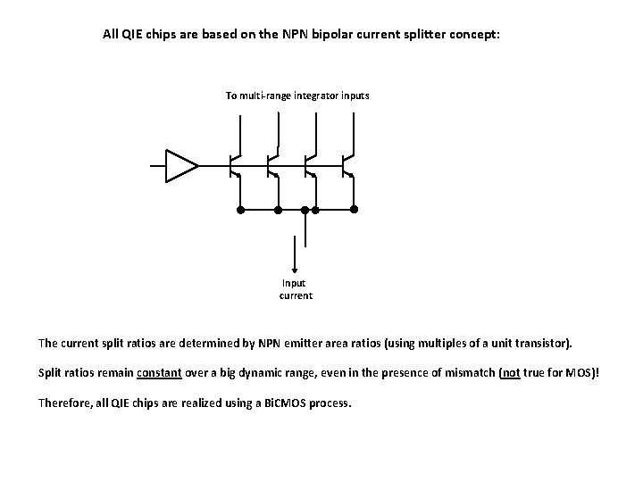
All QIE chips are based on the NPN bipolar current splitter concept: To multi-range integrator inputs Input current The current split ratios are determined by NPN emitter area ratios (using multiples of a unit transistor). Split ratios remain constant over a big dynamic range, even in the presence of mismatch (not true for MOS)! Therefore, all QIE chips are realized using a Bi. CMOS process.

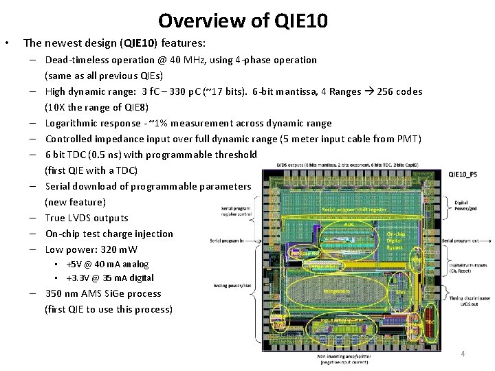
Overview of QIE 10 • The newest design (QIE 10) features: – Dead-timeless operation @ 40 MHz, using 4 -phase operation (same as all previous QIEs) – High dynamic range: 3 f. C – 330 p. C (~17 bits). 6 -bit mantissa, 4 Ranges 256 codes (10 X the range of QIE 8) – Logarithmic response - ~1% measurement across dynamic range – Controlled impedance input over full dynamic range (5 meter input cable from PMT) – 6 bit TDC (0. 5 ns) with programmable threshold (first QIE with a TDC) – Serial download of programmable parameters (new feature) – True LVDS outputs – On-chip test charge injection – Low power: 320 m. W • +5 V @ 40 m. A analog • +3. 3 V @ 35 m. A digital – 350 nm AMS Si. Ge process (first QIE to use this process) 4

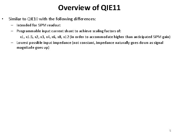
Overview of QIE 11 • Similar to QIE 10 with the following differences: – Intended for Si. PM readout – Programmable input current shunt to achieve scaling factors of: x 1, x 1. 5, x 2, x 3, x 4, x 6, x 8, x 12 (in order to accommodate higher than anticipated Si. PM gain) – Lowest possible input impedance (not constant, impedance naturally goes down as signal magnitude goes up) 5

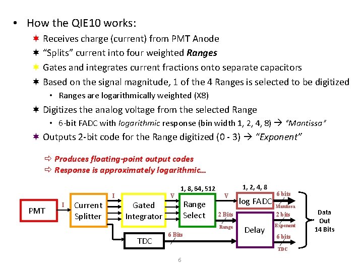
• How the QIE 10 works: ¬ Receives charge (current) from PMT Anode ¬ “Splits” current into four weighted Ranges ¬ Gates and integrates current fractions onto separate capacitors ¬ Based on the signal magnitude, 1 of the 4 Ranges is selected to be digitized • Ranges are logarithmically weighted (X 8) ¬ Digitizes the analog voltage from the selected Range • 6 -bit FADC with logarithmic response (bin width 1, 2, 4, 8) “Mantissa” ¬ Outputs 2 -bit code for the Range digitized (0 - 3) “Exponent” ð Produces floating-point output codes ð Response is approximately logarithmic… V I PMT I Current Splitter 1, 8, 64, 512 Range Select Gated Integrator 1, 2, 4, 8 V 2 Bits Range TDC 6 Bits log FADC 6 bits Mantissa 2 bits Delay Exponent 6 bits TDC 6 Data Out 14 Bits

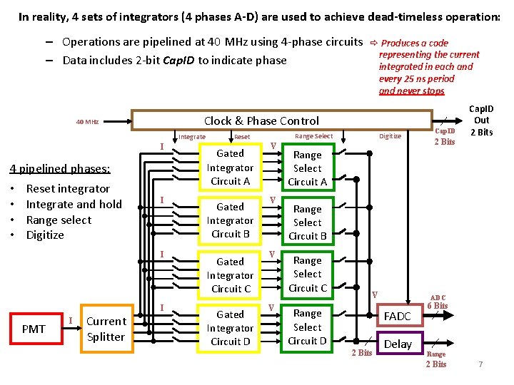
In reality, 4 sets of integrators (4 phases A-D) are used to achieve dead-timeless operation: – Operations are pipelined at 40 MHz using 4 -phase circuits – Data includes 2 -bit Cap. ID to indicate phase Clock & Phase Control 40 MHz Integrate Reset integrator Integrate and hold Range select Digitize Gated Integrator Circuit A I Gated Integrator Circuit B I I PMT I Current Splitter Range Select Reset I 4 pipelined phases: • • ð Produces a code representing the current integrated in each and every 25 ns period and never stops Gated Integrator Circuit C Gated Integrator Circuit D V V Digitize Cap. ID 2 Bits Cap. ID Out 2 Bits Range Select Circuit A Range Select Circuit B Range Select Circuit C V Range Select Circuit D ADC FADC 2 Bits Delay 6 Bits Range 2 Bits 7

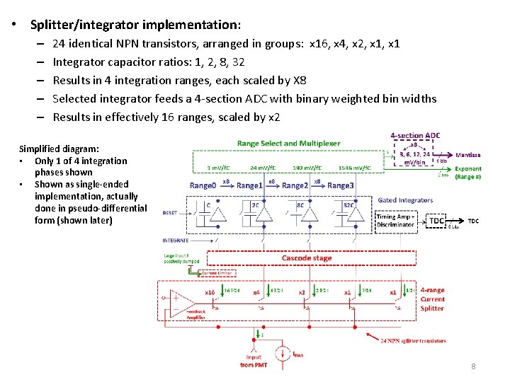
• Splitter/integrator implementation: – – – 24 identical NPN transistors, arranged in groups: x 16, x 4, x 2, x 1 Integrator capacitor ratios: 1, 2, 8, 32 Results in 4 integration ranges, each scaled by X 8 Selected integrator feeds a 4 -section ADC with binary weighted bin widths Results in effectively 16 ranges, scaled by x 2 Simplified diagram: • Only 1 of 4 integration phases shown • Shown as single-ended implementation, actually done in pseudo-differential form (shown later) 8

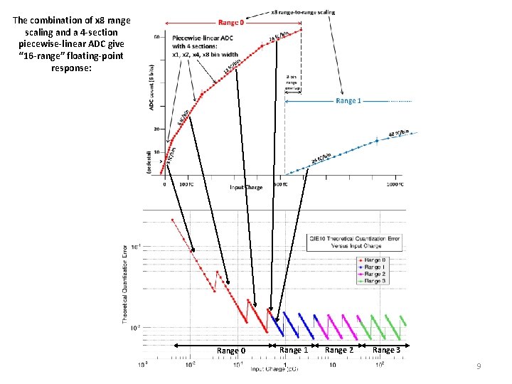
The combination of x 8 range scaling and a 4 -section piecewise-linear ADC give “ 16 -range” floating-point response: Range 0 Range 1 Range 2 Range 3 9

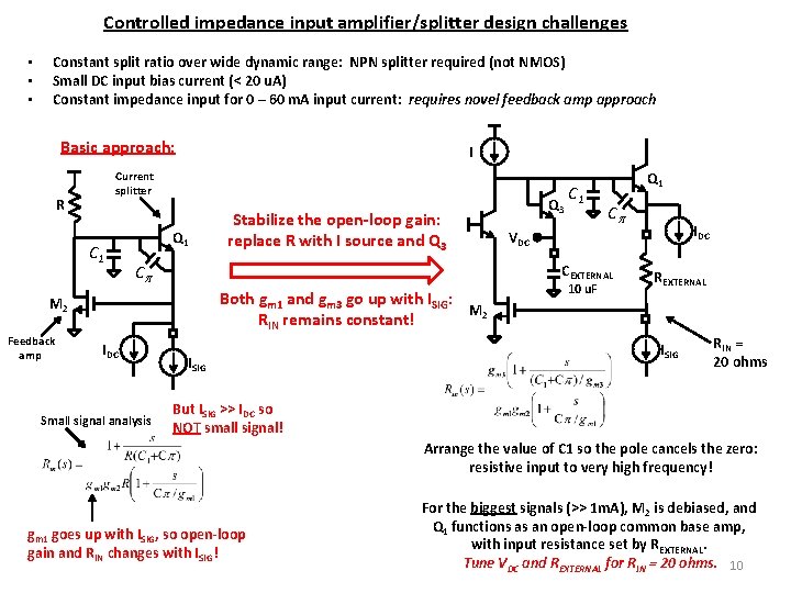
Controlled impedance input amplifier/splitter design challenges • • • Constant split ratio over wide dynamic range: NPN splitter required (not NMOS) Small DC input bias current (< 20 u. A) Constant impedance input for 0 – 60 m. A input current: requires novel feedback amp approach Basic approach: I Current splitter R C 1 Q 1 C Both gm 1 and gm 3 go up with ISIG: M 2 RIN remains constant! IDC Small signal analysis C 1 C ISIG IDC VDC CEXTERNAL M 2 Feedback amp Stabilize the open-loop gain: replace R with I source and Q 3 Q 1 10 u. F REXTERNAL ISIG RIN = 20 ohms But ISIG >> IDC so NOT small signal! Arrange the value of C 1 so the pole cancels the zero: resistive input to very high frequency! gm 1 goes up with ISIG, so open-loop gain and RIN changes with ISIG! For the biggest signals (>> 1 m. A), M 2 is debiased, and Q 1 functions as an open-loop common base amp, with input resistance set by REXTERNAL. Tune VDC and REXTERNAL for RIN = 20 ohms. 10

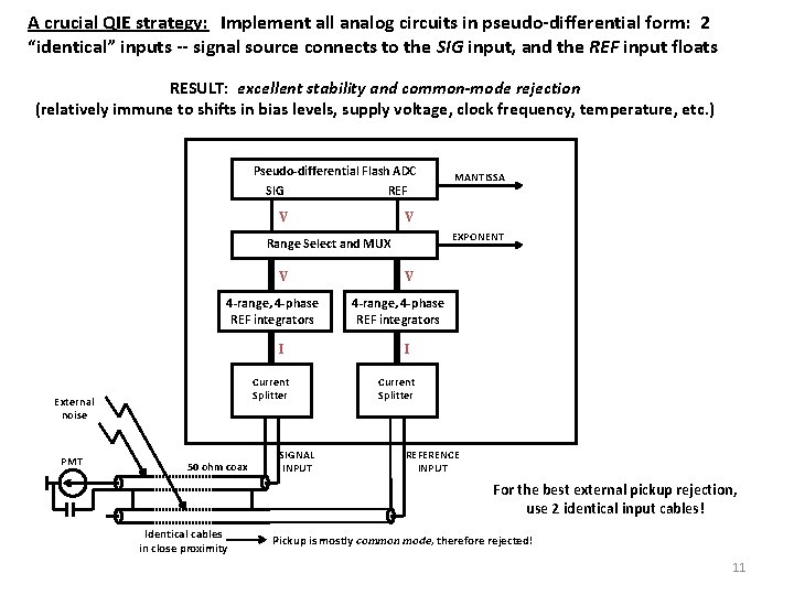
A crucial QIE strategy: Implement all analog circuits in pseudo-differential form: 2 “identical” inputs -- signal source connects to the SIG input, and the REF input floats RESULT: excellent stability and common-mode rejection (relatively immune to shifts in bias levels, supply voltage, clock frequency, temperature, etc. ) Pseudo-differential Flash ADC SIG REF V V EXPONENT Range Select and MUX V 4 -range, 4 -phase REF integrators I Current Splitter External noise PMT 50 ohm coax SIGNAL INPUT MANTISSA V 4 -range, 4 -phase REF integrators I Current Splitter REFERENCE INPUT For the best external pickup rejection, use 2 identical input cables! Identical cables in close proximity Pickup is mostly common mode, therefore rejected! 11

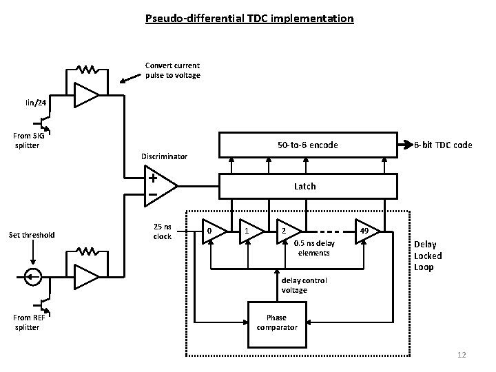
Pseudo-differential TDC implementation Convert current pulse to voltage Iin/24 From SIG splitter 50 -to-6 encode 6 -bit TDC code Discriminator Latch Set threshold 25 ns clock 0 1 2 49 0. 5 ns delay elements Delay Locked Loop delay control voltage From REF splitter Phase comparator 12

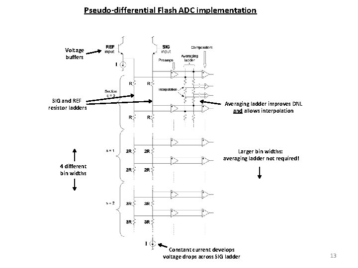
Pseudo-differential Flash ADC implementation Voltage buffers SIG and REF resistor ladders Averaging ladder improves DNL and allows interpolation Larger bin widths: averaging ladder not required! 4 different bin widths Constant current develops voltage drops across SIG ladder 13

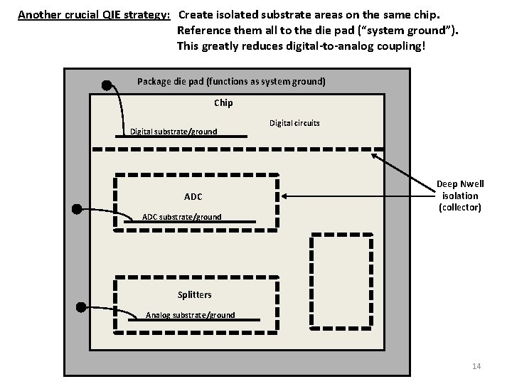
Another crucial QIE strategy: Create isolated substrate areas on the same chip. Reference them all to the die pad (“system ground”). This greatly reduces digital-to-analog coupling! Package die pad (functions as system ground) Chip Digital substrate/ground ADC substrate/ground Digital circuits Deep Nwell isolation (collector) Splitters Analog substrate/ground 14

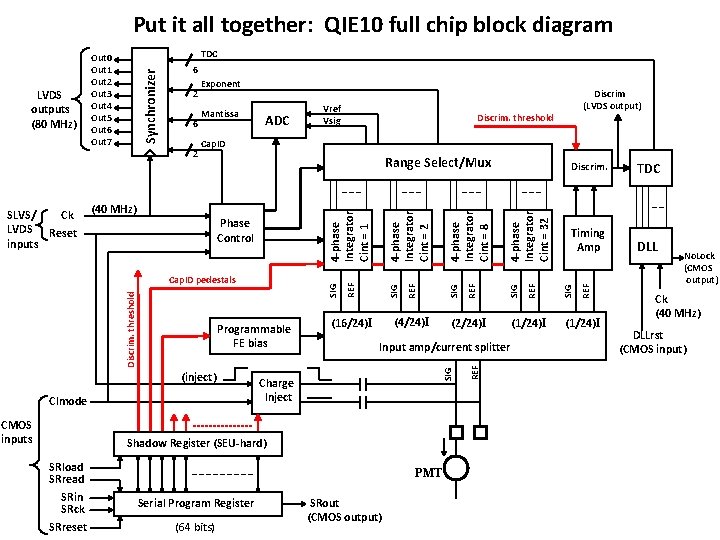
Put it all together: QIE 10 full chip block diagram 6 ADC Cap. ID CImode Charge Inject SRreset PMT Serial Program Register (64 bits) SRout (CMOS output) REF (1/24)I TDC Timing Amp DLL REF Discrim. SIG REF 4 -phase Integrator Cint = 32 Input amp/current splitter Shadow Register (SEU-hard) SRload SRread SRin SRck SIG 4 -phase Integrator Cint = 8 (2/24)I SIG (inject) (4/24)I (16/24)I REF SIG Discrim. threshold Programmable FE bias SIG Phase Control REF (40 MHz) Range Select/Mux Cap. ID pedestals CMOS inputs Discrim (LVDS output) Discrim. threshold 4 -phase Integrator Cint = 2 2 Mantissa Vref Vsig SIG 6 Exponent REF 2 4 -phase Integrator Cint = 1 SLVS/ Ck LVDS Reset inputs Synchronizer LVDS outputs (80 MHz) TDC Out 0 Out 1 Out 2 Out 3 Out 4 Out 5 Out 6 Out 7 (1/24)I No. Lock (CMOS output) Ck (40 MHz) DLLrst (CMOS input)

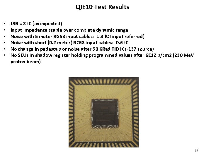
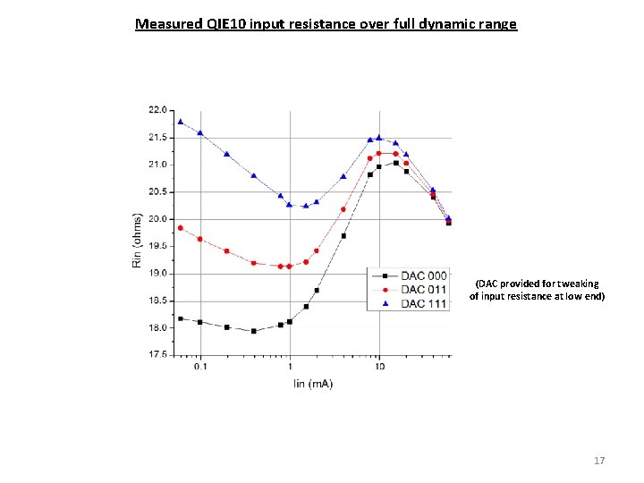
QIE 10 Test Results • • • LSB = 3 f. C (as expected) Input impedance stable over complete dynamic range Noise with 5 meter RG 58 input cables: 1. 8 f. C (input referred) Noise with short (0. 2 meter) RC 58 input cables: 0. 6 f. C No change in pedestals or noise after 50 KRad TID (Cs-137 source) No SEUs in shadow register holding programmed values after 6 E 12 p/cm 2 (230 Me. V proton beam) 16

Measured QIE 10 input resistance over full dynamic range (DAC provided for tweaking of input resistance at low end) 17

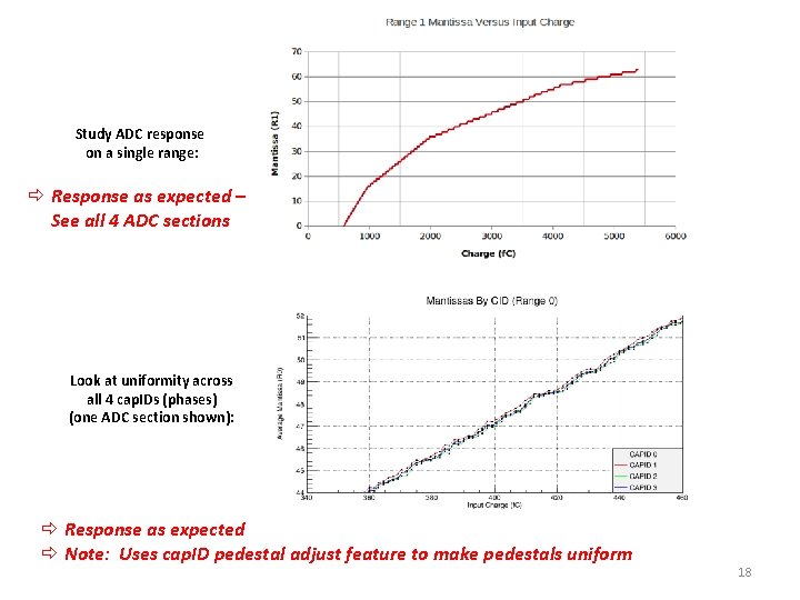
Study ADC response on a single range: ð Response as expected – See all 4 ADC sections Look at uniformity across all 4 cap. IDs (phases) (one ADC section shown): ð Response as expected ð Note: Uses cap. ID pedestal adjust feature to make pedestals uniform 18

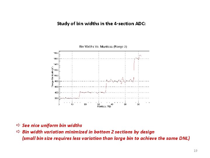
Study of bin widths in the 4 -section ADC: ð See nice uniform bin widths ð Bin width variation minimized in bottom 2 sections by design (small bin size requires less variation than large bin to achieve the same DNL) 19

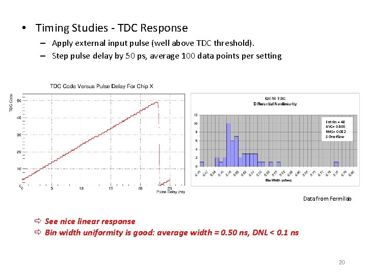
• Timing Studies - TDC Response – Apply external input pulse (well above TDC threshold). – Step pulse delay by 50 ps, average 100 data points per setting Entries = 48 AVG= 0. 500 RMS= 0. 082 1 Overflow Data from Fermilab ð See nice linear response ð Bin width uniformity is good: average width = 0. 50 ns, DNL < 0. 1 ns 20

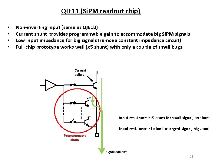
QIE 11 (Si. PM readout chip) • • Non-inverting input (same as QIE 10) Current shunt provides programmable gain to accommodate big Si. PM signals Low input impedance for big signals (remove constant impedance circuit) Full-chip prototype works well (x 5 shunt) with only a couple of small bugs Current splitter Input resistance ~15 ohms for small signal, no shunt Input resistance ~1 ohm for largest signal, big shunt Programmable shunt Signal current 21

QIE: a success story over 25 years! Future QIE work this year: • • Modification of QIE 11 for ATLAS: add another bit of resolution (7 -bit mantissa) Quad QIE (4 per package)? ? 22