Power Minimization using Simultaneous Gate Sizing DualVdd and
- Slides: 24

Power Minimization using Simultaneous Gate Sizing, Dual-Vdd and Dual-Vth Assignment Ashish Srivastava, Dennis Sylvester, David Blaauw

Outline o o o Introduction Preliminary Algorithm Experimental Results Conclusions

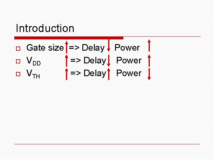
Introduction o o o Gate size => Delay Power VDD => Delay Power VTH => Delay Power

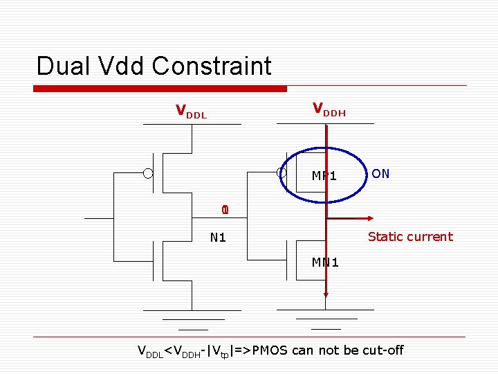
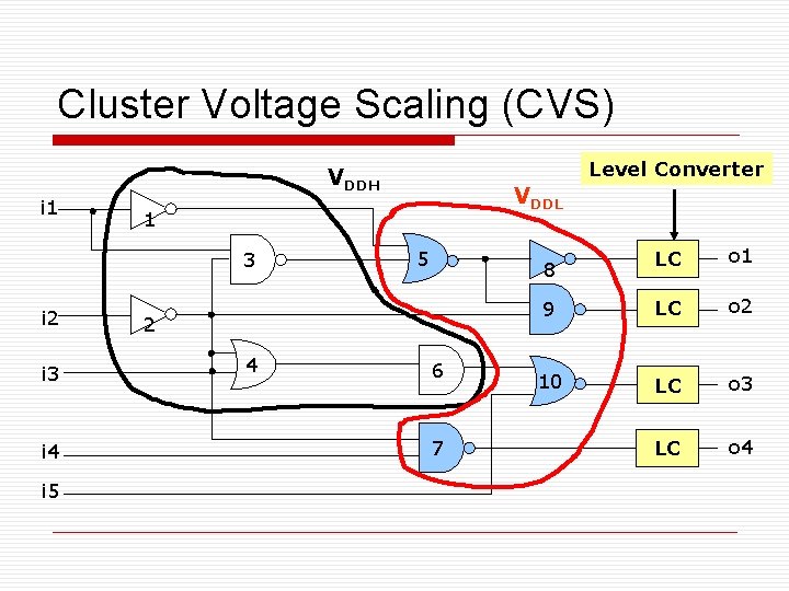
Outline o o Introduction Preliminary n n o o o Dual Vdd constraint Cluster Voltage Scaling (CVS) Algorithm Experimental Results Conclusions

Dual Vdd Constraint VDDH VDDL MP 1 ON 1 0 Static current N 1 MN 1 VDDL<VDDH-|Vtp|=>PMOS can not be cut-off

Cluster Voltage Scaling (CVS) Level Converter VDDH i 1 1 3 i 2 i 3 i 4 i 5 VDDL 5 2 4 LC o 1 9 LC o 2 10 LC o 3 LC o 4 8 6 7

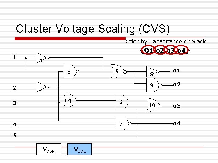
Cluster Voltage Scaling (CVS) Order by Capacitance or Slack {O 1, o 2, o 3, o 4} i 1 1 5 3 i 2 8 2 4 i 3 6 7 i 4 i 5 VDDH VDDL o 1 9 o 2 10 o 3 o 4

Outline o o o Introduction Preliminary Algorithm - VVS n n o o Backward Pass Frontward Pass Experimental Results Conclusions

Outline o o o Introduction Preliminary Algorithm n n o o Backward Pass Frontward Pass Experimental Results Conclusions

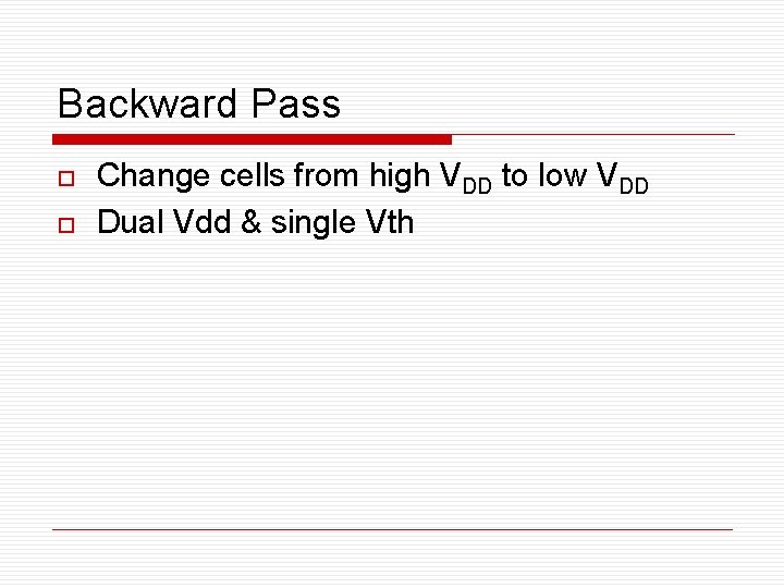
Backward Pass o o Change cells from high VDD to low VDD Dual Vdd & single Vth

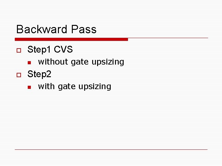
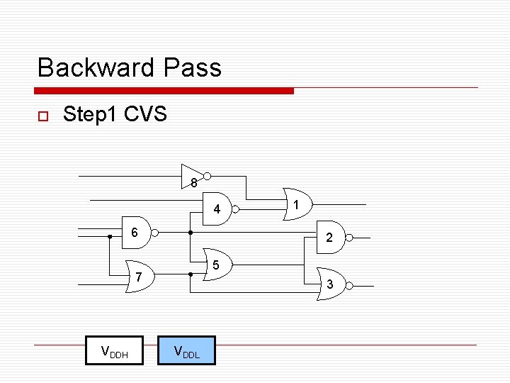
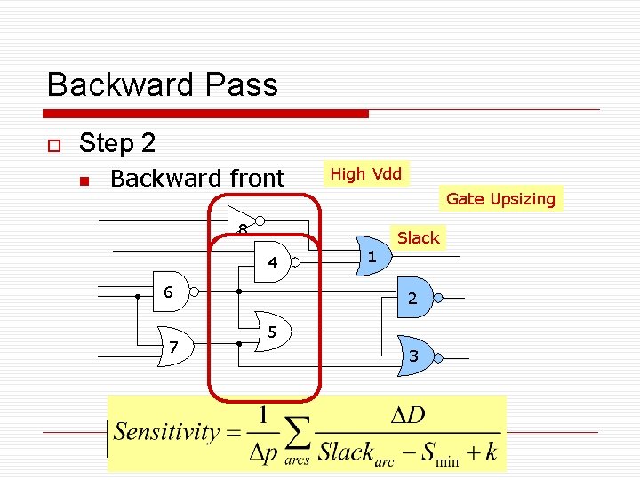
Backward Pass o Step 1 CVS n o without gate upsizing Step 2 n with gate upsizing

Backward Pass o Step 1 CVS 8 4 6 2 5 7 VDDH 1 3 VDDL

Backward Pass o Step 2 n Backward front High Vdd Gate Upsizing 8 4 6 2 5 7 VDDH 1 Slack 3 VDDL

Backward Pass o o Escape local minima. Find the globe minima. The front between high and low Vdd gates is in the best position in terms of the total power dissipation for a dual Vdd, single Vth.

Outline o o o Introduction Preliminary Algorithm n n o o Backward Pass Frontward Pass Experimental Results Conclusions

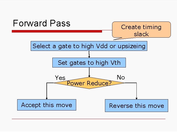
Forward Pass Create timing slack Select a gate to high Vdd or upsizeing Set gates to high Vth Yes Power Reduce? Accept this move No Reverse this move

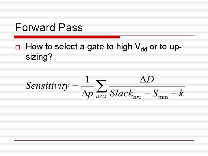
Forward Pass o How to select a gate to high Vdd or to upsizing?

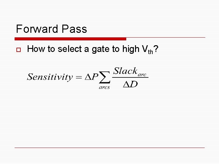
Forward Pass o How to select a gate to high Vth?

Outline o o o Introduction Preliminary Algorithm Experimental Results Conclusions

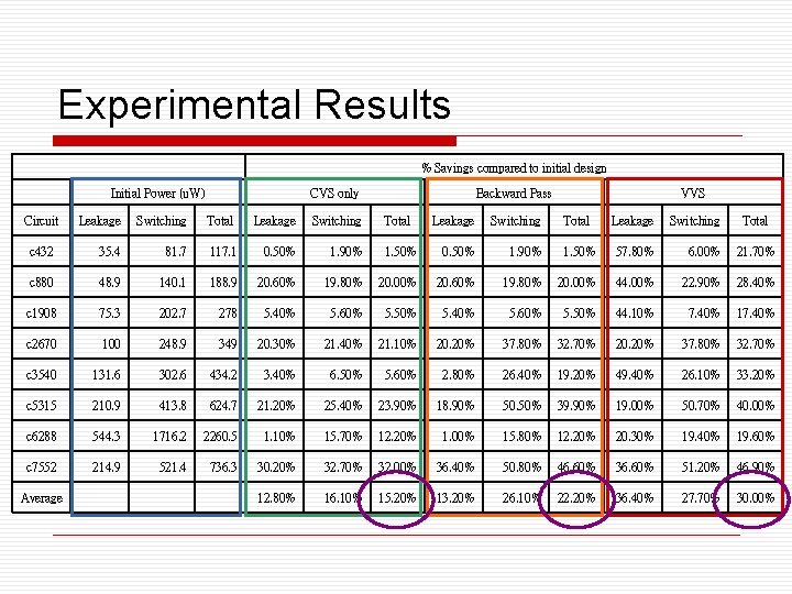
Experimental Results Circuit % Savings compared to initial design Initial Power (u. W) Leakage Switching c 432 35. 4 81. 7 c 880 48. 9 c 1908 CVS only Leakage Switching 117. 1 0. 50% 1. 90% 1. 50% 0. 50% 140. 1 188. 9 20. 60% 19. 80% 20. 00% 75. 3 202. 7 278 5. 40% 5. 60% c 2670 100 248. 9 349 20. 30% c 3540 131. 6 302. 6 434. 2 c 5315 210. 9 413. 8 c 6288 544. 3 c 7552 Average Total Backward Pass Total VVS Total Leakage Switching Total 1. 90% 1. 50% 57. 80% 6. 00% 21. 70% 20. 60% 19. 80% 20. 00% 44. 00% 22. 90% 28. 40% 5. 50% 5. 40% 5. 60% 5. 50% 44. 10% 7. 40% 17. 40% 21. 10% 20. 20% 37. 80% 32. 70% 3. 40% 6. 50% 5. 60% 2. 80% 26. 40% 19. 20% 49. 40% 26. 10% 33. 20% 624. 7 21. 20% 25. 40% 23. 90% 18. 90% 50. 50% 39. 90% 19. 00% 50. 70% 40. 00% 1716. 2 2260. 5 1. 10% 15. 70% 12. 20% 1. 00% 15. 80% 12. 20% 20. 30% 19. 40% 19. 60% 214. 9 521. 4 736. 3 30. 20% 32. 70% 32. 00% 36. 40% 50. 80% 46. 60% 36. 60% 51. 20% 46. 90% 12. 80% 16. 10% 15. 20% 13. 20% 26. 10% 22. 20% 36. 40% 27. 70% 30. 00%

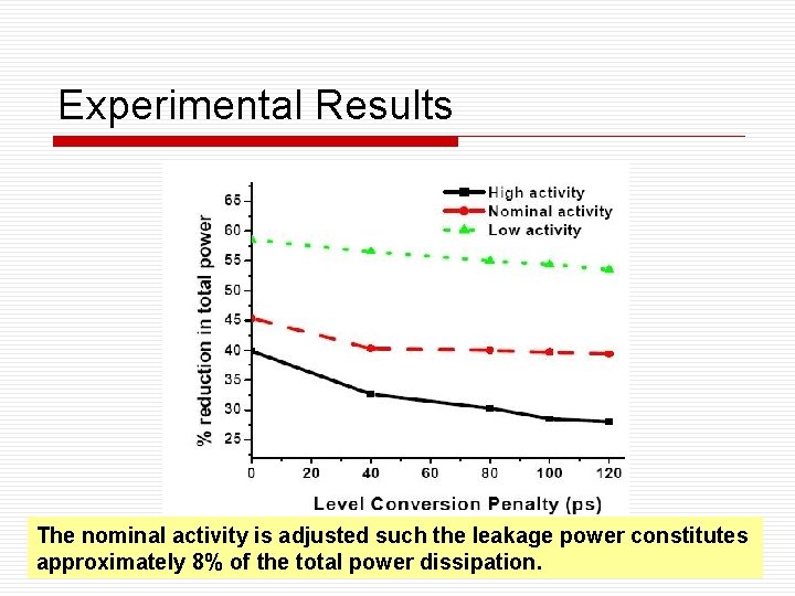
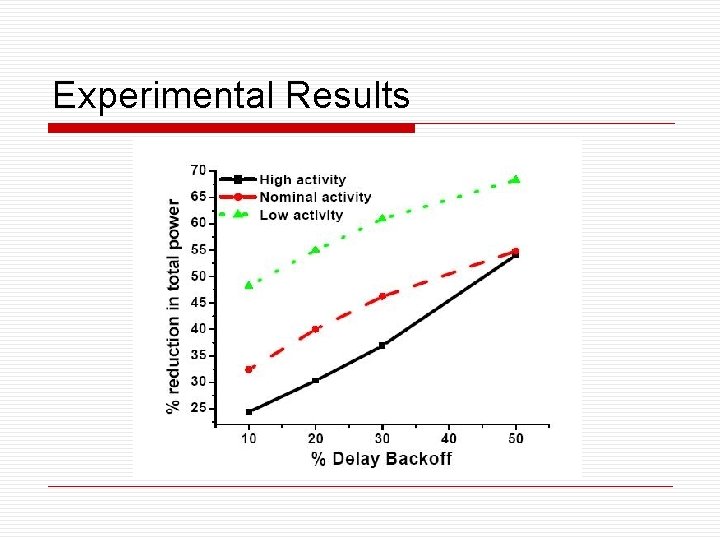
Experimental Results The nominal activity is adjusted such the leakage power constitutes approximately 8% of the total power dissipation.

Experimental Results

Outline o o o Introduction Preliminary Algorithm Experimental Results Conclusions

Conclusions o The VVS algorithm combines gate sizing with Vdd and Vth assignment to minimize the total power dissipation.