Photonic crystals for light trapping in solar cells
- Slides: 32

Photonic crystals for light trapping in solar cells Jo Gjessing 1, 2, 3, Erik S. Marstein 1, 2, Einar Haugan 1, Håvard Granlund 4, and Aasmund S. Sudbø*, 2, 3 Institute for Energy Technology, Department of Solar Energy, Kjeller 2027, Norway 2 University of Oslo, Department of Physics, P. O. Box 1048 Blindern, Oslo 0316, Norway 3 University Graduate Center at Kjeller, P. O. Box 70, Kjeller 2027, Norway 4 Department of Physics, Norwegian University Science and Technology, Trondheim 7491, Norway *aas@unik. no 1

Outline • • Introduction Light trapping in silicon solar cells 2 D photonic crystals for light trapping Simulation results – Photogenerated current density – Diffraction efficiencies – Different unit cells structures • Fabrication and characterization – First demonstration: Standard silicon fab – More cost-effective fabrication • Conclusions

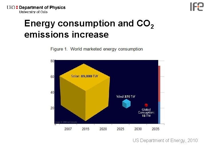
Energy consumption and CO 2 emissions increase US Department of Energy, 2010

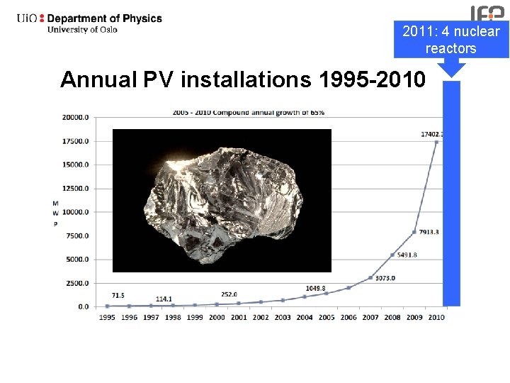
2011: 4 nuclear reactors Annual PV installations 1995 -2010

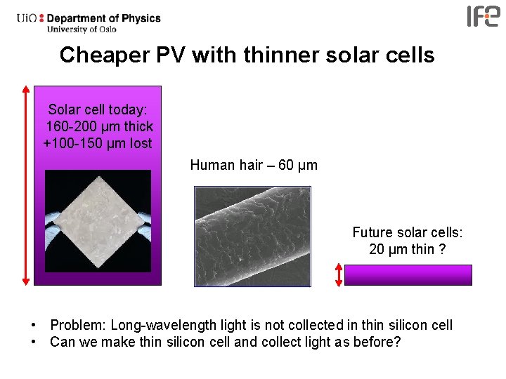
Cheaper PV with thinner solar cells Solar cell today: 160 -200 µm thick +100 -150 µm lost Human hair – 60 µm Future solar cells: 20 µm thin ? • Problem: Long-wavelength light is not collected in thin silicon cell • Can we make thin silicon cell and collect light as before?

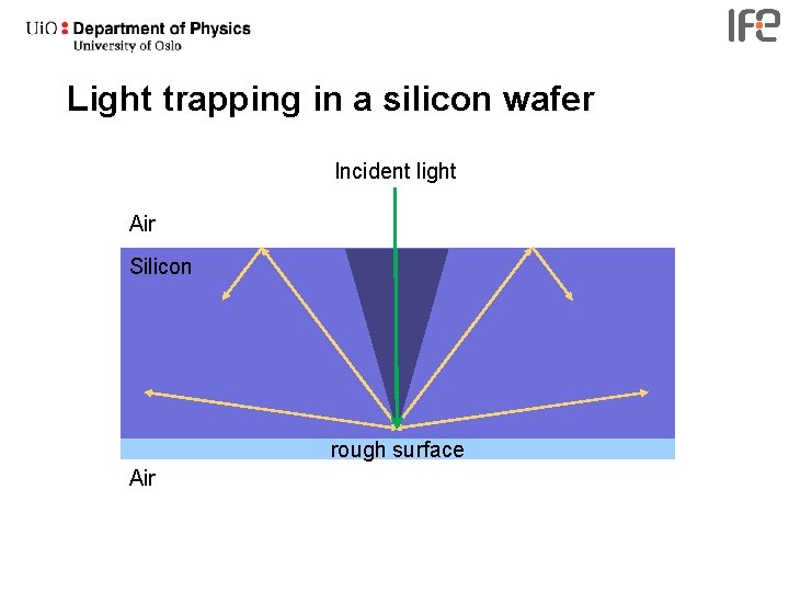
Light trapping in a silicon wafer Incident light Air Silicon rough surface Air

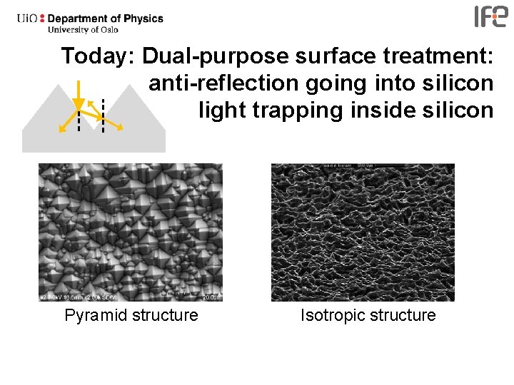
Today: Dual-purpose surface treatment: anti-reflection going into silicon light trapping inside silicon Pyramid structure Isotropic structure

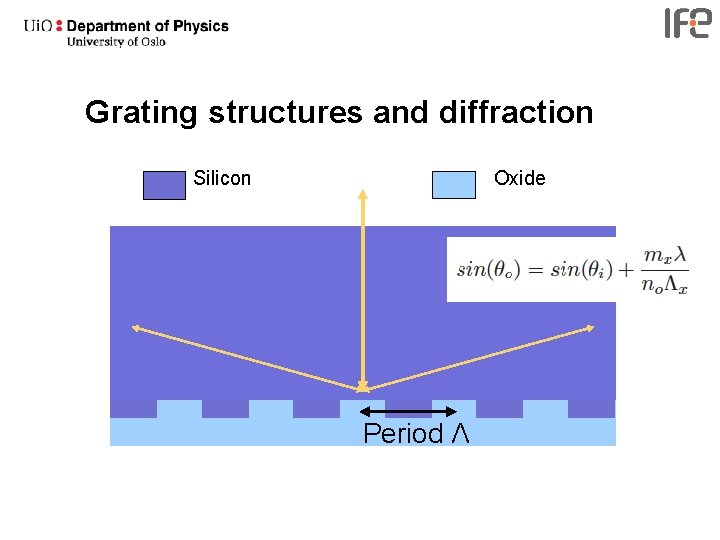
Grating structures and diffraction Silicon Oxide Period Λ

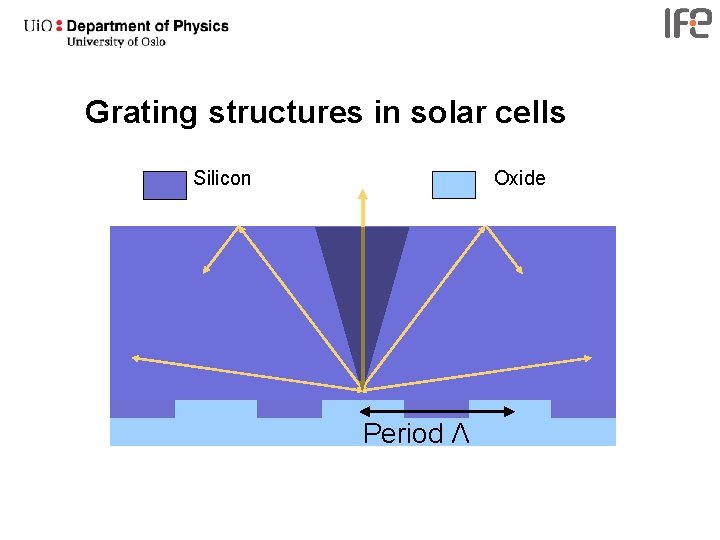
Grating structures in solar cells Silicon Oxide Period Λ

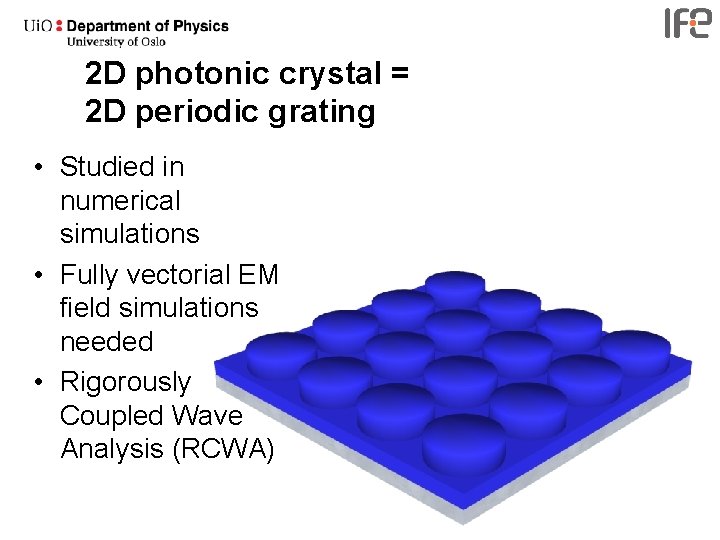
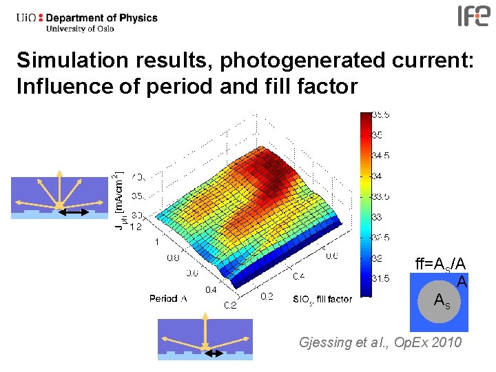
2 D photonic crystal = 2 D periodic grating • Studied in numerical simulations • Fully vectorial EM field simulations needed • Rigorously Coupled Wave Analysis (RCWA)

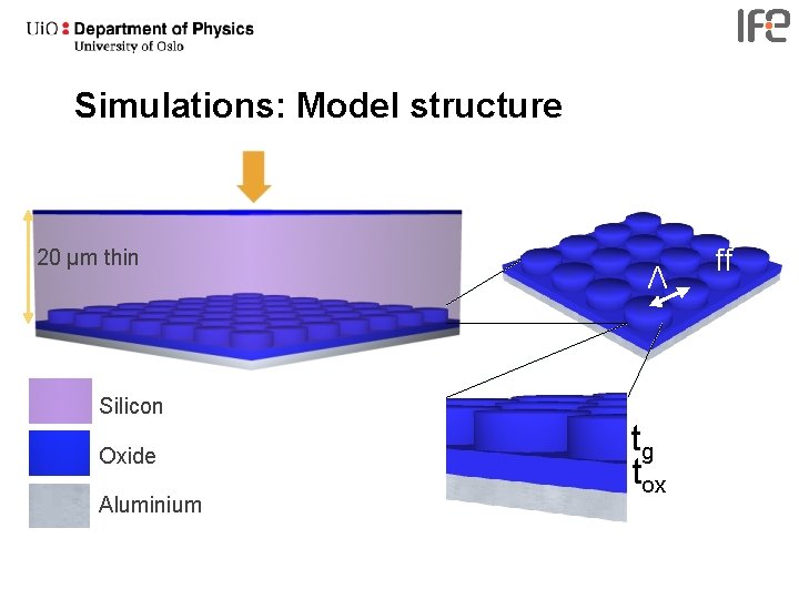
Simulations: Model structure 20 µm thin Λ Silicon Oxide Aluminium tg tox ff

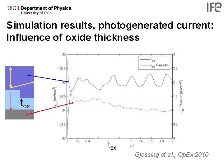
Simulation results, photogenerated current: Influence of oxide thickness tox Gjessing et al. , Op. Ex 2010

Simulation results, photogenerated current: Influence of period and fill factor ff=As/A A As Gjessing et al. , Op. Ex 2010

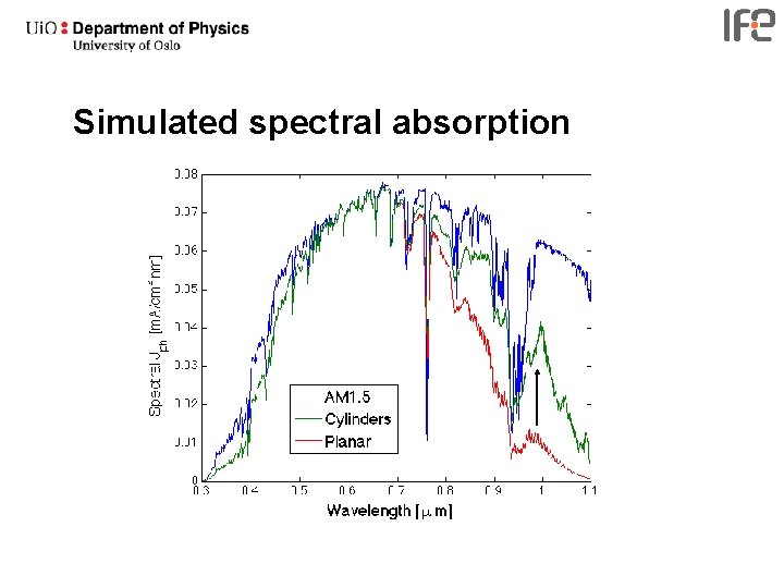
Simulated spectral absorption

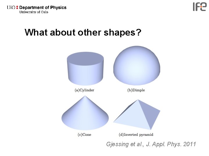
What about other shapes? Gjessing et al. , J. Appl. Phys. 2011

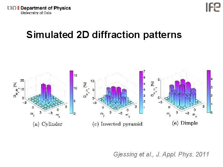
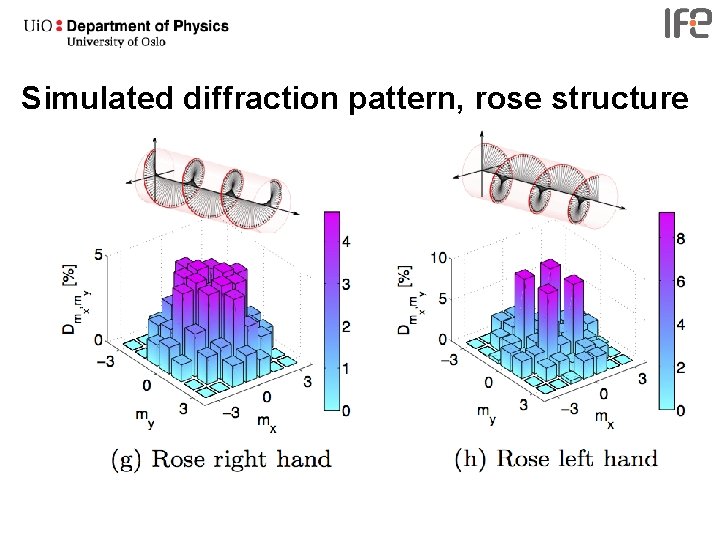
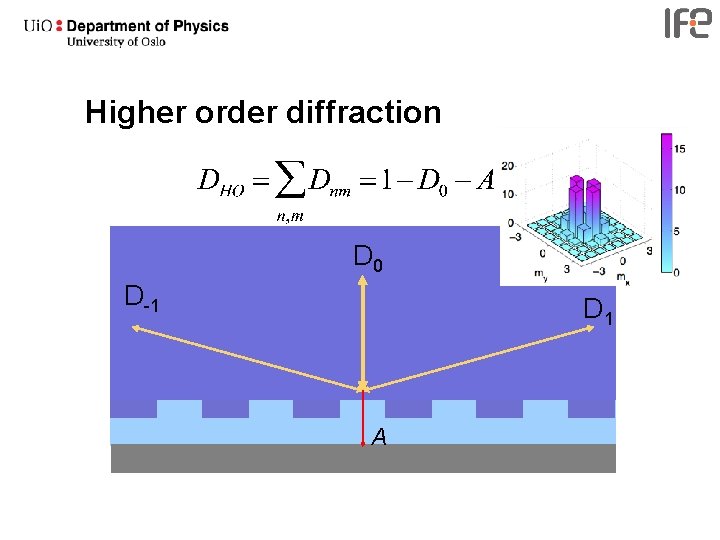
Simulated 2 D diffraction patterns Gjessing et al. , J. Appl. Phys. 2011

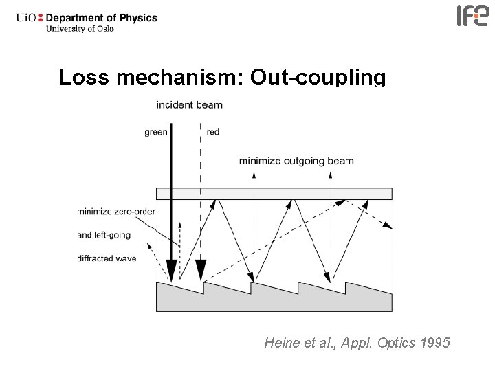
Loss mechanism: Out-coupling Heine et al. , Appl. Optics 1995

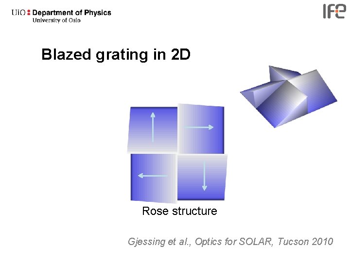
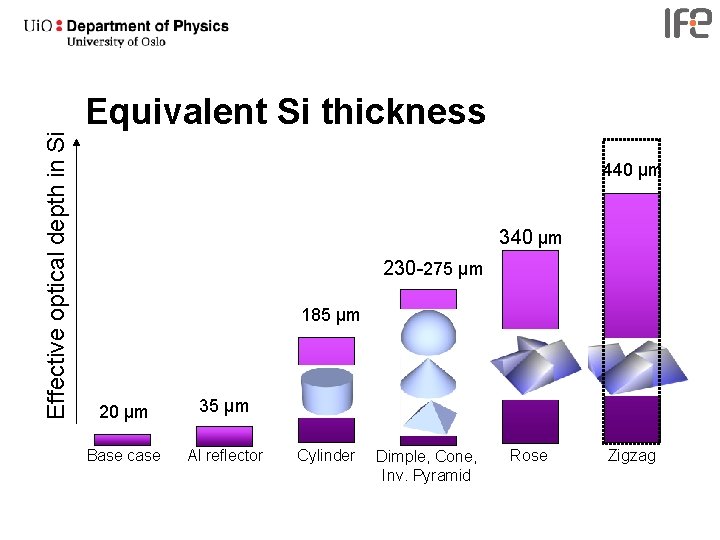
Blazed grating in 2 D Rose structure Gjessing et al. , Optics for SOLAR, Tucson 2010

Simulated diffraction pattern, rose structure

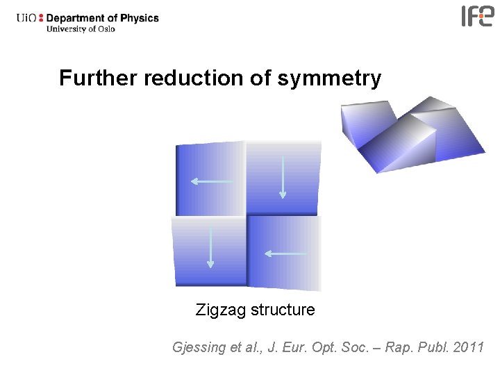
Further reduction of symmetry Zigzag structure Gjessing et al. , J. Eur. Opt. Soc. – Rap. Publ. 2011

Effective optical depth in Si Equivalent Si thickness 440 µm 340 µm 230 -275 µm 185 µm 20 µm 35 µm Base case Al reflector Cylinder Dimple, Cone, Inv. Pyramid Rose Zigzag

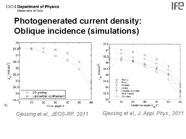
Photogenerated current density: Oblique incidence (simulations) Gjessing et al. , JEOS-RP, 2011 Gjessing et al. , J. Appl. Phys. , 2011

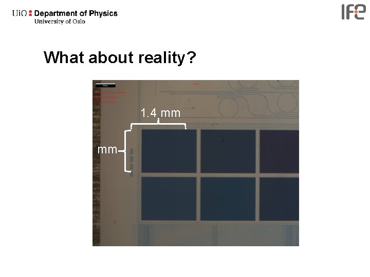
What about reality? 1. 4 mm 1 mm

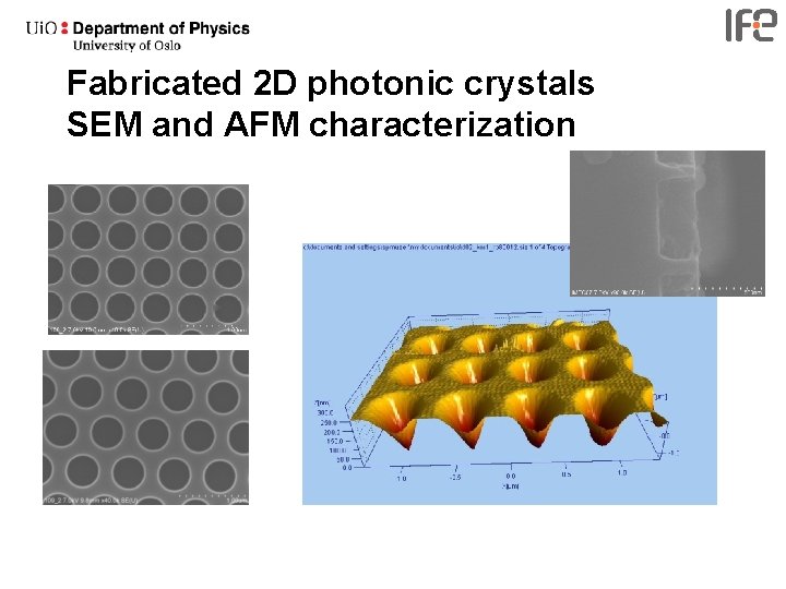
Fabricated 2 D photonic crystals SEM and AFM characterization

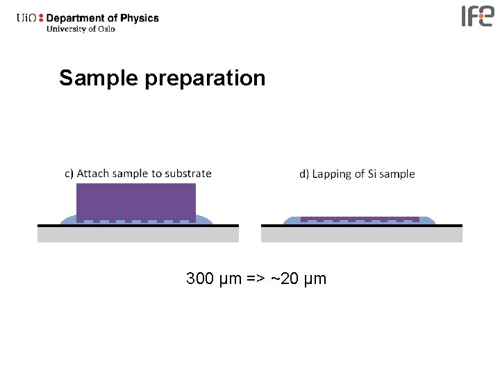
Sample preparation 300 µm => ~20 µm

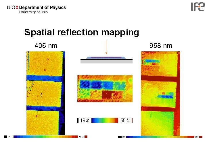
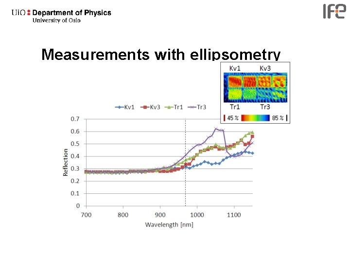
Spatial reflection mapping 406 nm 968 nm

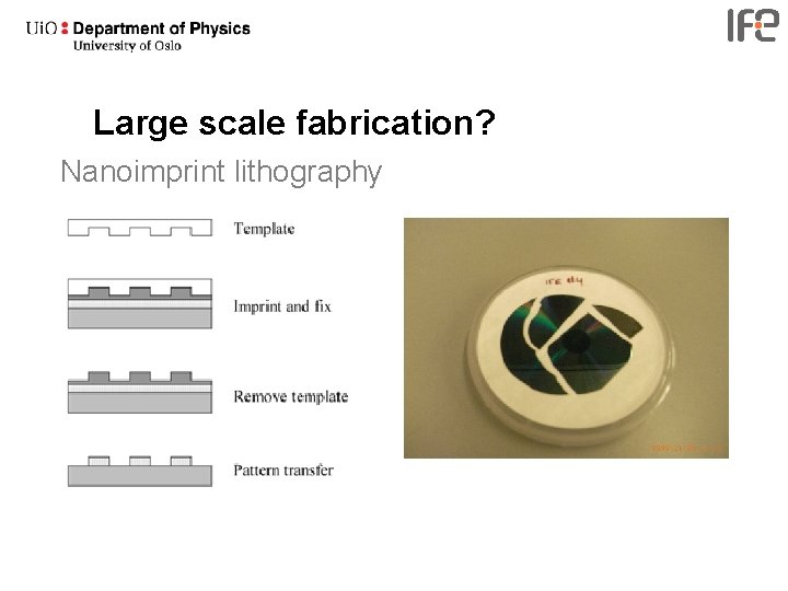
Large scale fabrication? Nanoimprint lithography

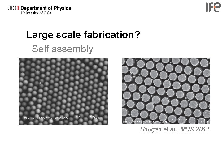
Large scale fabrication? Self assembly Haugan et al. , MRS 2011

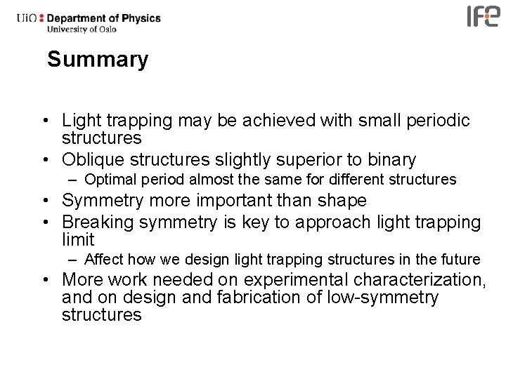
Summary • Light trapping may be achieved with small periodic structures • Oblique structures slightly superior to binary – Optimal period almost the same for different structures • Symmetry more important than shape • Breaking symmetry is key to approach light trapping limit – Affect how we design light trapping structures in the future • More work needed on experimental characterization, and on design and fabrication of low-symmetry structures

Thank you for your attention Jo. gjessing@ife. no www. ife. no → Solenergi Thanks to and for funding

Measurements with ellipsometry

Higher order diffraction D 0 D-1 D 1 A