Nanotechnology Principles Applications and Careers National Educators Workshop
- Slides: 42
Nanotechnology Principles, Applications, and Careers National Educators Workshop November 3, 2013 SHINE: Seattle’s Hub for Industry-driven Nanotechnology Education
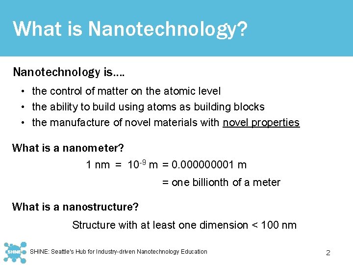
What is Nanotechnology? Nanotechnology is…. • the control of matter on the atomic level • the ability to build using atoms as building blocks • the manufacture of novel materials with novel properties What is a nanometer? 1 nm = 10 -9 m = 0. 00001 m = one billionth of a meter What is a nanostructure? Structure with at least one dimension < 100 nm SHINE: Seattle’s Hub for Industry-driven Nanotechnology Education 2
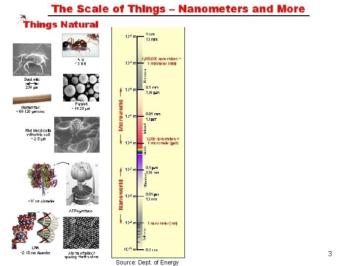
3 3 Source: Dept. of Energy
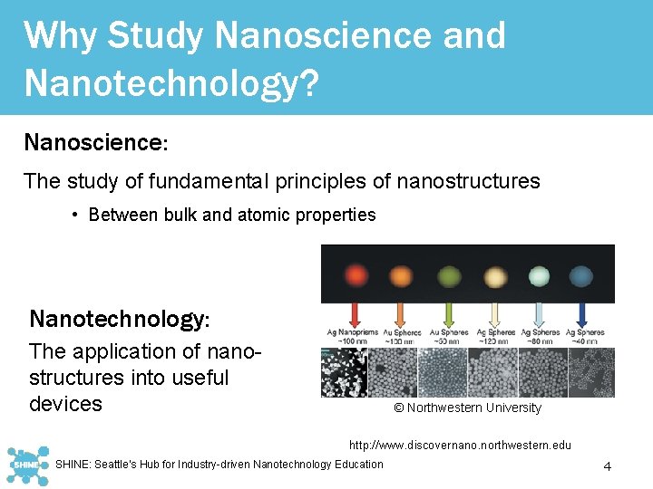
Why Study Nanoscience and Nanotechnology? Nanoscience: The study of fundamental principles of nanostructures • Between bulk and atomic properties Nanotechnology: The application of nanostructures into useful devices © Northwestern University http: //www. discovernano. northwestern. edu SHINE: Seattle’s Hub for Industry-driven Nanotechnology Education 4
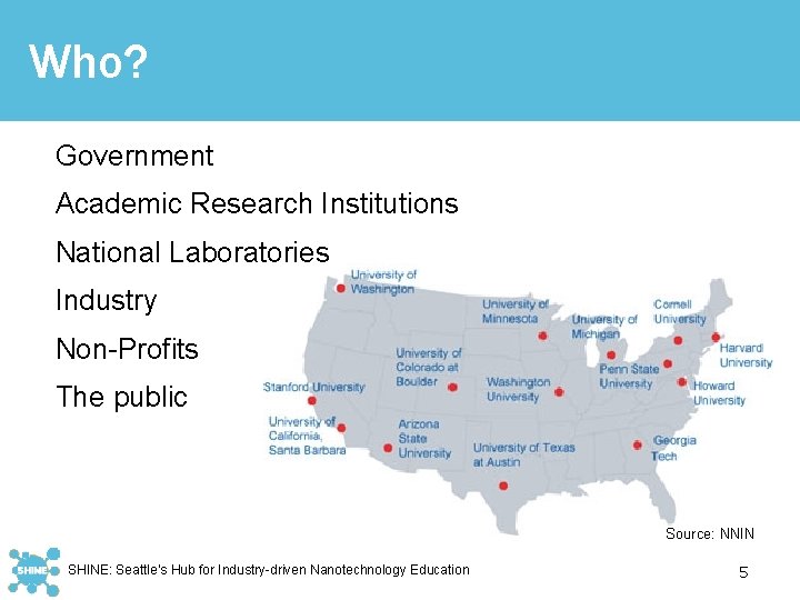
Who? Government Academic Research Institutions National Laboratories Industry Non-Profits The public Source: NNIN SHINE: Seattle’s Hub for Industry-driven Nanotechnology Education 5
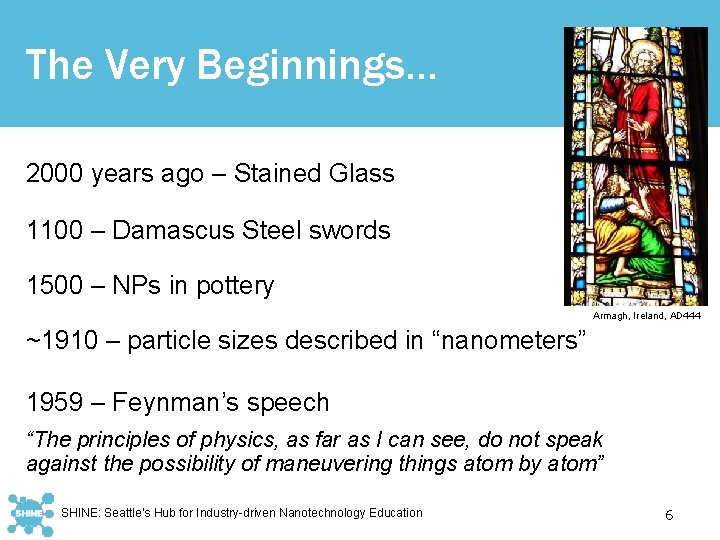
The Very Beginnings… 2000 years ago – Stained Glass 1100 – Damascus Steel swords 1500 – NPs in pottery Armagh, Ireland, AD 444 ~1910 – particle sizes described in “nanometers” 1959 – Feynman’s speech “The principles of physics, as far as I can see, do not speak against the possibility of maneuvering things atom by atom” SHINE: Seattle’s Hub for Industry-driven Nanotechnology Education 6
Then… 1970 – “Nanotechnology” coined (Taniguchi) 1981 – First atoms seen (Binnig and Rohrer, STM) 1986 – Engines of Creation, the Coming Age of Nanotechnology by Richard Drexler “Nanotechnology is the principle of atom manipulation atom by atom, through control of the structure of matter at the molecular level. It entails the ability to build molecular systems with atom-by-atom precision, yielding a variety of nanomachines” SHINE: Seattle’s Hub for Industry-driven Nanotechnology Education 7
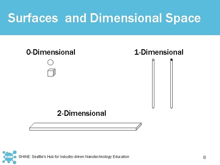
Surfaces and Dimensional Space 0 -Dimensional 1 -Dimensional 2 -Dimensional SHINE: Seattle’s Hub for Industry-driven Nanotechnology Education 8
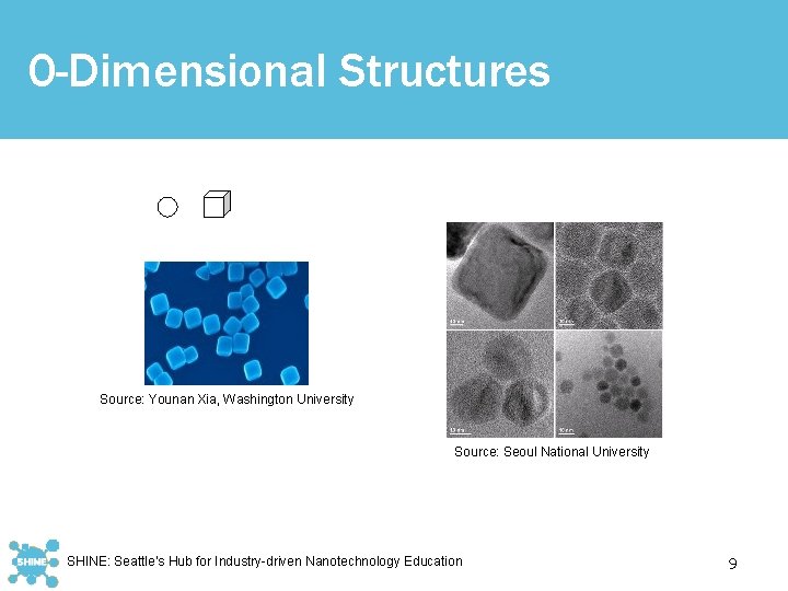
0 -Dimensional Structures Source: Younan Xia, Washington University Source: Seoul National University SHINE: Seattle’s Hub for Industry-driven Nanotechnology Education 9
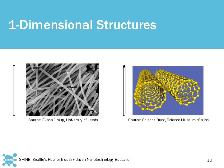
1 -Dimensional Structures Source: Evans Group, University of Leeds Source: Science Buzz, Science Museum of Minn. SHINE: Seattle’s Hub for Industry-driven Nanotechnology Education 10
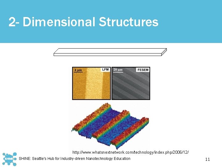
2 - Dimensional Structures http: //www. whatsnextnetwork. com/technology/index. php/2006/12/ SHINE: Seattle’s Hub for Industry-driven Nanotechnology Education 11
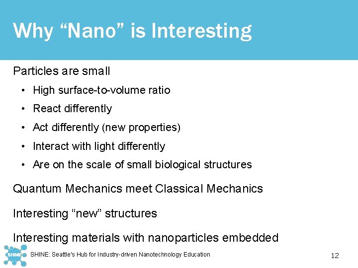
Why “Nano” is Interesting Particles are small • High surface-to-volume ratio • React differently • Act differently (new properties) • Interact with light differently • Are on the scale of small biological structures Quantum Mechanics meet Classical Mechanics Interesting “new” structures Interesting materials with nanoparticles embedded SHINE: Seattle’s Hub for Industry-driven Nanotechnology Education 12
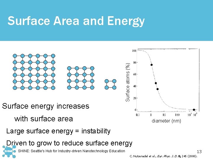
Surface energy increases with surface area Surface atoms (%) Surface Area and Energy diameter (nm) Large surface energy = instability Driven to grow to reduce surface energy SHINE: Seattle’s Hub for Industry-driven Nanotechnology Education 13 C. Nutzenadel et al. , Eur. Phys. J. D. 8, 245 (2000).
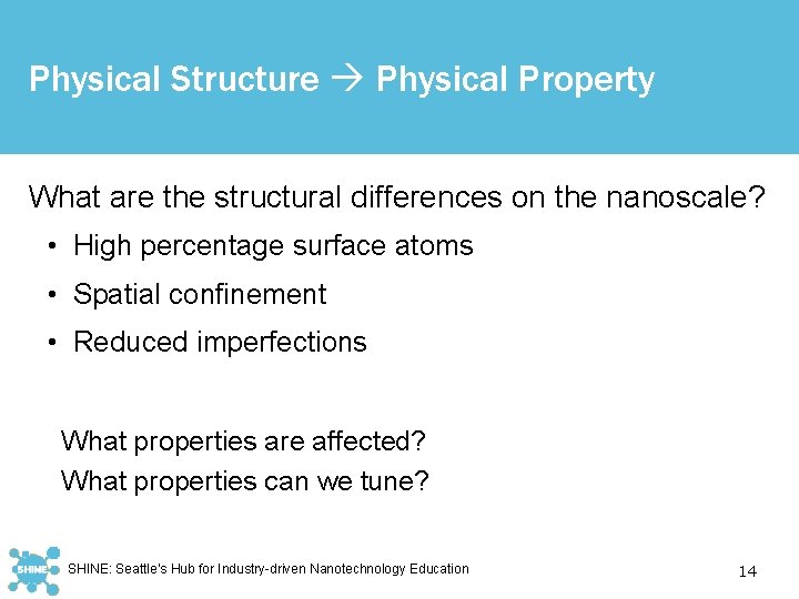
Physical Structure Physical Property What are the structural differences on the nanoscale? • High percentage surface atoms • Spatial confinement • Reduced imperfections What properties are affected? What properties can we tune? SHINE: Seattle’s Hub for Industry-driven Nanotechnology Education 14
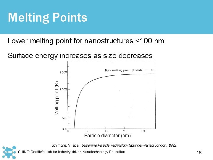
Melting Points Lower melting point for nanostructures <100 nm Melting point (K) Surface energy increases as size decreases Particle diameter (nm) Ichimose, N. et al. Superfine Particle Technology Springer-Verlag London, 1992. SHINE: Seattle’s Hub for Industry-driven Nanotechnology Education 15
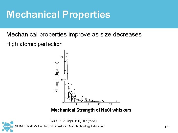
Mechanical Properties Mechanical properties improve as size decreases Strength (kg/mm) High atomic perfection d (µm) Mechanical Strength of Na. Cl whiskers Gyulai, Z. Z. Phys. 138, 317 (1954). SHINE: Seattle’s Hub for Industry-driven Nanotechnology Education 16
Electrical Properties Electron Scattering • Electrons move through a metal to conduct electricity • Electrons are scattered to cause resistivity • Decreasing size fewer defects less scattering Surface Scattering • Electrons scatter against the surface of nanostructure Widening of band gap SHINE: Seattle’s Hub for Industry-driven Nanotechnology Education 17
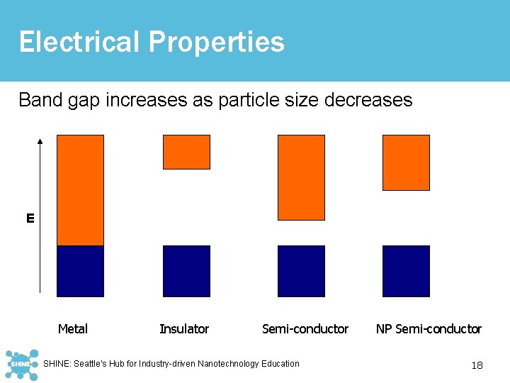
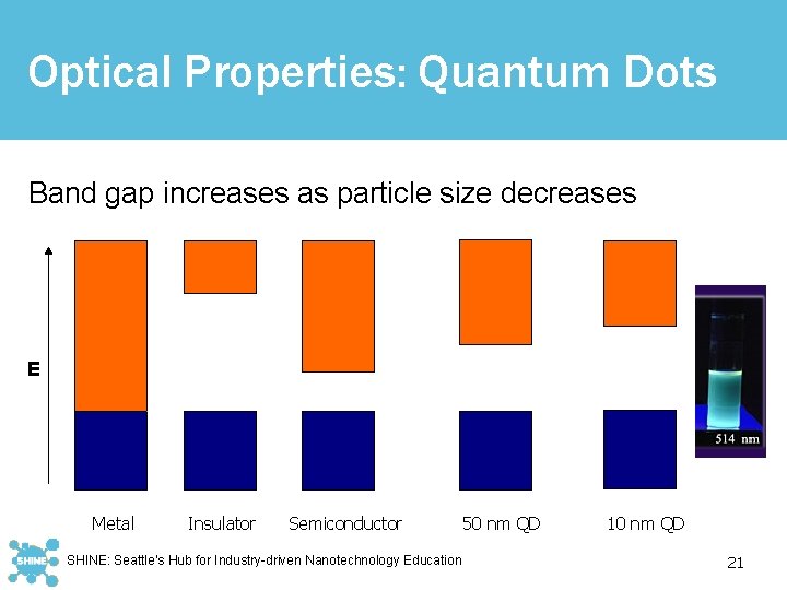
Electrical Properties Band gap increases as particle size decreases E Metal Insulator Semi-conductor SHINE: Seattle’s Hub for Industry-driven Nanotechnology Education NP Semi-conductor 18
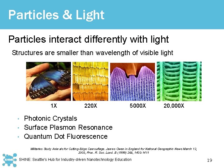
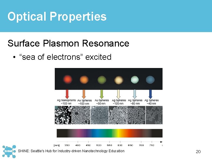
Particles & Light Particles interact differently with light Structures are smaller than wavelength of visible light 1 X 220 X 5000 X 20, 000 X Photonic Crystals • Surface Plasmon Resonance • Quantum Dot Fluorescence • Militaries Study Animals for Cutting-Edge Camouflage. James Owen in England for National Geographic News March 12, 2003, Proc. R. Soc. Lond. B (1999) 266, 1403 -1411 SHINE: Seattle’s Hub for Industry-driven Nanotechnology Education 19
Optical Properties Surface Plasmon Resonance • “sea of electrons” excited SHINE: Seattle’s Hub for Industry-driven Nanotechnology Education 20
Optical Properties: Quantum Dots Band gap increases as particle size decreases E Metal Insulator Semiconductor SHINE: Seattle’s Hub for Industry-driven Nanotechnology Education 50 nm QD 10 nm QD 21
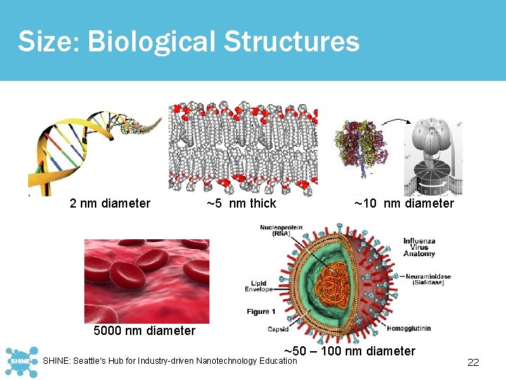
Size: Biological Structures 2 nm diameter ~5 nm thick ~10 nm diameter 5000 nm diameter ~50 – 100 nm diameter SHINE: Seattle’s Hub for Industry-driven Nanotechnology Education 22
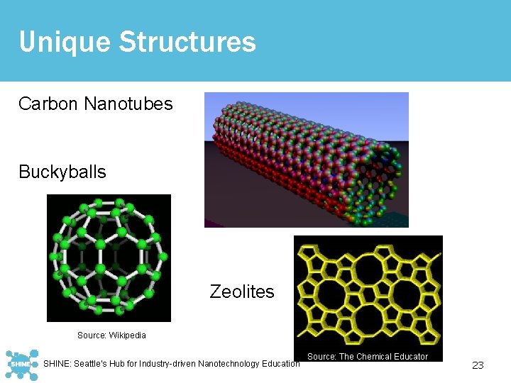
Unique Structures Carbon Nanotubes Buckyballs Source: Wikipedia Zeolites Source: Wikipedia SHINE: Seattle’s Hub for Industry-driven Nanotechnology Education Source: The Chemical Educator 23
Image References Slide 3 The Scale of Things. [Online image]. 09 Aug. 2010. <http: //www. er. doe. gov/bes/scale_of_things. html>. Slide 5 Silver and Gold Particles. [Online image]. 09 Aug. 2010 <http: //www. discovernano. northwestern. edu/whatis/index_html/sizematters_html> Slide 6 NNIN Sites. [Online image]. 09 Aug. 2010. <http: //www. nnin. org/nnin_site. html>. Slide 10 Nanocages. [Online image]. 09 Aug. 2010. <http: //www. nanocages. com>. Nanoparticle Shape Modification. [Online image]. 09 Aug. 2010. <http: //kshong. snu. ac. kr/research_nanoparticle. html>. Slide 11 Nanowires. [Online image]. Molecular & Nanoscale Physics Group. 09 Aug. 2010. <http: //www. mnp. leeds. ac. uk/sdevans/Evans_Nano. html>. Nanotubes. [Online image]. Science Museum of Minnesota. 09 Aug. 2010. <http: //www. smm. org/buzz/museum/ask/greaney/starting>. Slide 14 C. Nutzenadel et al. , Eur. Phys. J. D. 8, 245 (2000). SHINE: Seattle’s Hub for Industry-driven Nanotechnology Education 24
Slide 16 Ichimose, N. et al. Superfine Particle Technology Springer-Verlag London, 1992. Slide 17 Gyulai, Z. Z. Phys. 138, 317 (1954). Slide 20 News Militaries Study Animals for Cutting-Edge Camouflage. James Owen in England for National Geographic March 12, Proc. R. Soc. Lond. B (1999) 266, 1403 -1411 (Penn State NACK Educational Resources, 2009). Slide 21 Silver and Gold Particles. [Online image]. 09 Aug. 2010 <http: //www. discovernano. northwestern. edu/whatis/index_html/sizematters_html>. Slide 23 Red blood cells. [Online image]. 09 Aug. 2010 <http: //www. topnews. in/health/files/Red-Blood-Cells. jpg>. DNA double helix. [Online image]. 09 Aug. 2010 <http: //www. biojobblog. com/uploads/image/dna_500. jpg>. Lipid bilayer. [Online image]. 09 Aug. 2010 <http: //upload. wikimedia. org/wikipedia/commons/f/f 0/Lipid_bilayer_section. gif>. Image References This material is based upon work supported by the National Science Foundation under Grant Number 1204279. Any opinions, findings, and conclusions or recommendations expressed in this material are those of the author(s) and do not 25 necessarily reflect the views of the National Science Foundation.
Applications of Nanotechnology SHINE: Seattle’s Hub for Industry-driven Nanotechnology Education
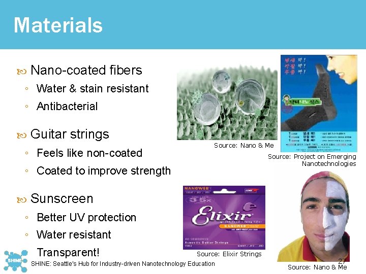
Materials Nano-coated fibers ◦ Water & stain resistant ◦ Antibacterial Guitar strings ◦ Feels like non-coated Source: Nano & Me Source: Project on Emerging Nanotechnologies ◦ Coated to improve strength Sunscreen ◦ Better UV protection ◦ Water resistant ◦ Transparent! Source: Elixir Strings SHINE: Seattle’s Hub for Industry-driven Nanotechnology Education 27 Source: Nano & Me
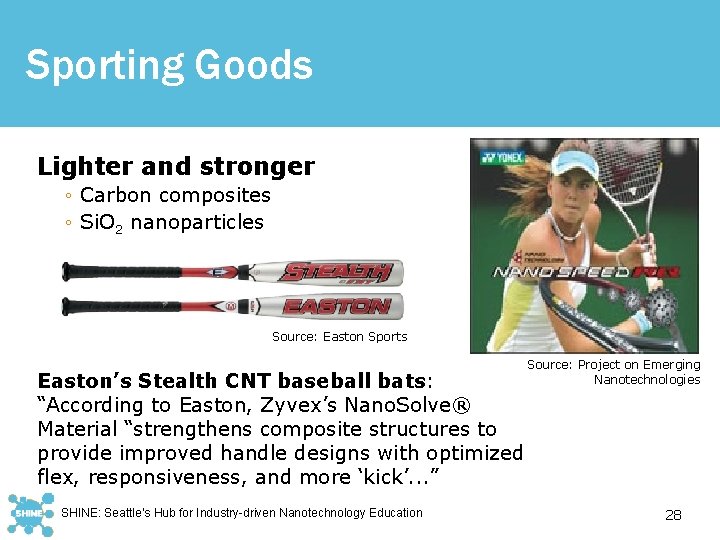
Sporting Goods Lighter and stronger ◦ Carbon composites ◦ Si. O 2 nanoparticles Source: Easton Sports Easton’s Stealth CNT baseball bats: “According to Easton, Zyvex’s Nano. Solve® Material “strengthens composite structures to provide improved handle designs with optimized flex, responsiveness, and more ‘kick’. . . ” SHINE: Seattle’s Hub for Industry-driven Nanotechnology Education Source: Project on Emerging Nanotechnologies 28
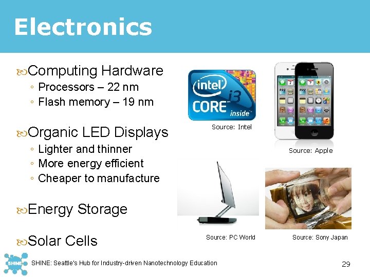
Electronics Computing Hardware ◦ Processors – 22 nm ◦ Flash memory – 19 nm Organic LED Displays ◦ Lighter and thinner ◦ More energy efficient ◦ Cheaper to manufacture Source: Intel Source: Apple Energy Storage Solar Cells Source: PC World SHINE: Seattle’s Hub for Industry-driven Nanotechnology Education Source: Sony Japan 29
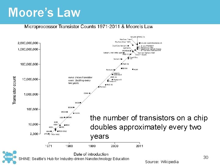
Moore’s Law the number of transistors on a chip doubles approximately every two years SHINE: Seattle’s Hub for Industry-driven Nanotechnology Education Source: Wikipedia 30
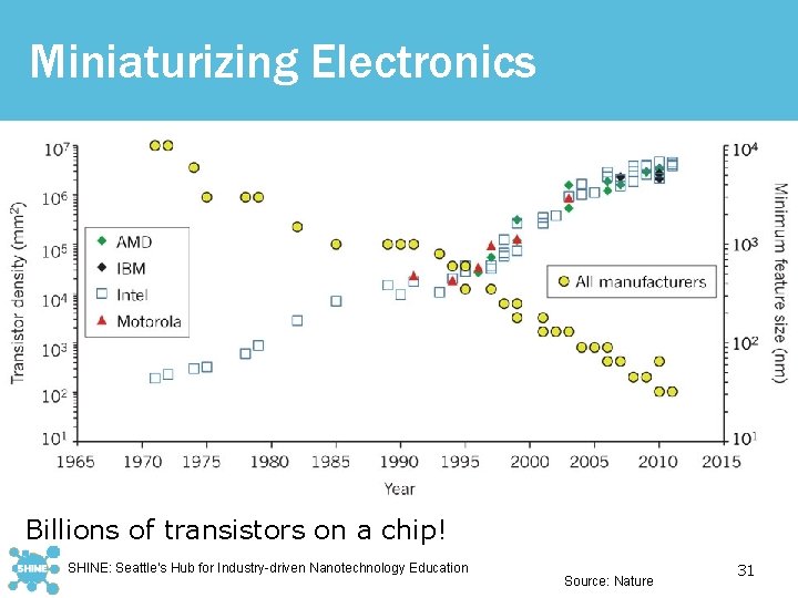
Miniaturizing Electronics Billions of transistors on a chip! SHINE: Seattle’s Hub for Industry-driven Nanotechnology Education Source: Nature 31
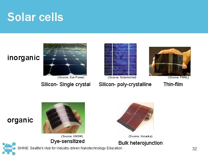
Solar cells inorganic (Source: Sun Power) Silicon- Single crystal organic (Source: Solarmrshal) Silicon- poly-crystalline (Source: PNNL) Thin-film Source: Reinforced Plastics (Source: UNSW) Dye-sensitized (Source: Konarka) Bulk heterojunction SHINE: Seattle’s Hub for Industry-driven Nanotechnology Education 32
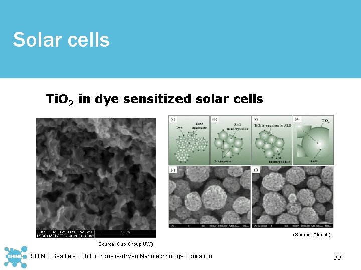
Solar cells Ti. O 2 in dye sensitized solar cells meso-porous Ti. O 2 film Source: Reinforced Plastics (Source: Aldrich) (Source: Cao Group UW) SHINE: Seattle’s Hub for Industry-driven Nanotechnology Education 33
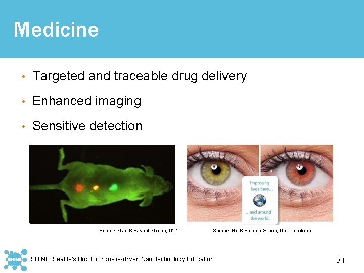
Medicine • Targeted and traceable drug delivery • Enhanced imaging • Sensitive detection Source: Gao Research Group, UW Source: Hu Research Group, Univ. of Akron SHINE: Seattle’s Hub for Industry-driven Nanotechnology Education 34
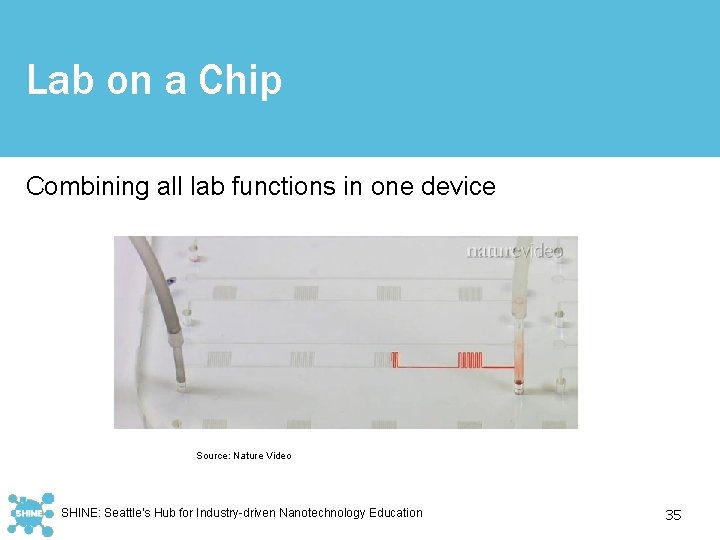
Lab on a Chip Combining all lab functions in one device Source: Nature Video SHINE: Seattle’s Hub for Industry-driven Nanotechnology Education 35
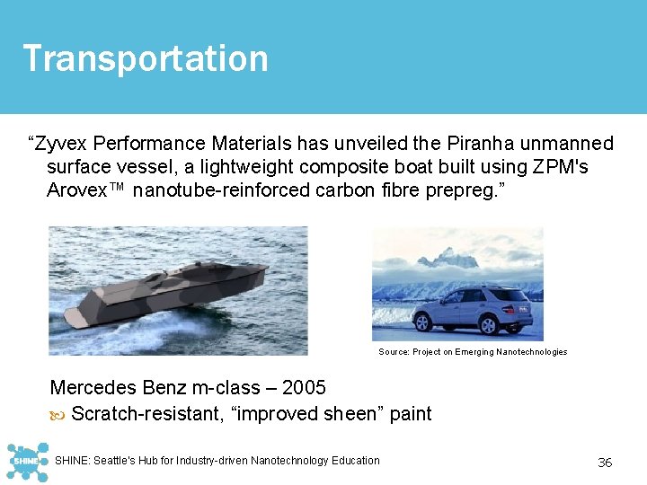
Transportation “Zyvex Performance Materials has unveiled the Piranha unmanned surface vessel, a lightweight composite boat built using ZPM's Arovex™ nanotube-reinforced carbon fibre prepreg. ” Source: Project on Emerging Nanotechnologies Source: Reinforced Plastics Mercedes Benz m-class – 2005 Scratch-resistant, “improved sheen” paint SHINE: Seattle’s Hub for Industry-driven Nanotechnology Education 36
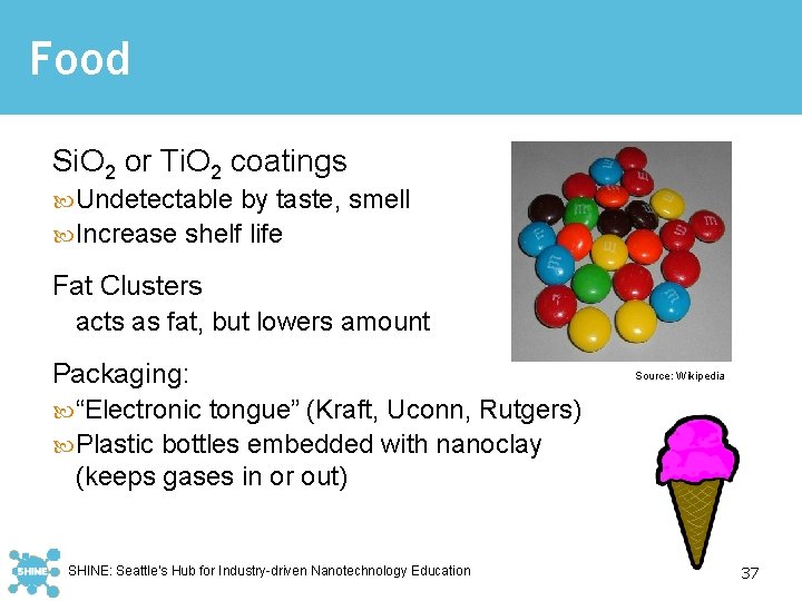
Food Si. O 2 or Ti. O 2 coatings Undetectable by taste, smell Increase shelf life Fat Clusters acts as fat, but lowers amount Packaging: “Electronic tongue” (Kraft, Uconn, Rutgers) Plastic bottles embedded with nanoclay (keeps gases in or out) SHINE: Seattle’s Hub for Industry-driven Nanotechnology Education Source: Wikipedia 37
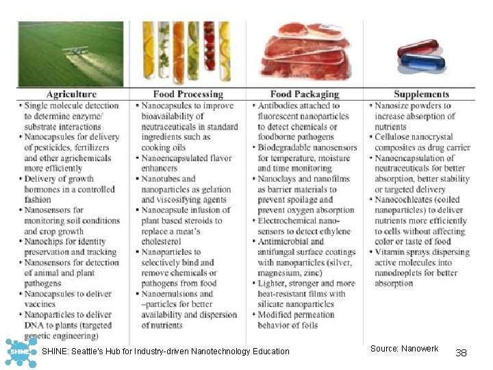
SHINE: Seattle’s Hub for Industry-driven Nanotechnology Education Source: Nanowerk 38
Image References Slide 2 Number of Nano Patents. [Online image]. 09 Aug. 2010. <http: //nanopatentsandinnovations. blogspot. com/2010/01/2009 -record-year-for-nanotechnology. html >. Slide 3 Lotus Effect. [Online image]. 09 Aug. 2010. <http: //www. nanoandme. org/nano-products/textiles-and-clothing/>. Nano. Silver Socks. [Online image]. 09 Aug. 2010. <http: //www. nanowerk. com/nanotechnology/ten_things_you_should_know_7. html>. Nano Web Strings. [Online image]. 09 Aug. 2010. <http: //www. elixirstrings. com/products/product_acoustic. html#nano>. Sunscreen. [Online image]. 09 Aug. 2010. <http: //www. nanoandme. org/nano-products/cosmetics-andsunscreen>. SHINE: Seattle’s Hub for Industry-driven Nanotechnology Education 39
Slide 4 Stealth CNT baseball bat. [Online image]. 09 Aug. 2010. <http: //www. bplowestprices. com/easton-2009 -lst 10 stealth-cnt-youth-baseball-bat-12. html>. Nanospeed tennis racquet. [Online image]. 09 Aug. 2010. <http: //www. nanotechproject. org/inventories/consumer/browse/products/yonex_nanospeed_rq_tennis_racquets />. Slide 5 iphone. [Online image]. 23 July. 2012. <http: //store. apple. com/us/browse/home/shop_iphone/family/iphone>. Intel Core i 3. [Online image]. 23 July. 2012. <http: //alldownloadforfree. blogspot. com/2012/05/differencebetween-core-i 3 -core-i 5 -and. html>. Flat screen LED Display. [Online image]. 09 Aug. 2010. <http: //www. dailytech. com/Slender+Beautiful+First+OLED+TV+Introduced/article 9108. htm>. Organic LED Display. [Online image]. 09 Aug. 2010. <http: //www. pcworld. com/article/132262/in_pictures_philips_and_sony_oled_displays. html>. Slide 6 Moore’s Law. [Online image]. 23 July. 2012. <http: //en. wikipedia. org/wiki/Moore%27 s_law>. Slide 7 Ferain, Isabelle, Cynthia A Colinge, and Jean-Pierre Colinge. "Multigate Transistors as the Future of Classical Metal-Oxide-Semiconductor Field-Effect Transistors. " Nature 479 (Nov. 2011): 310 -316. Nature. Web. 8 July 2013. <http: //www. nature. com/nature/journal/v 479/n 7373/full/nature 10676. html>. Image References SHINE: Seattle’s Hub for Industry-driven Nanotechnology Education 40
Slide 8 single crystal Si PV. [Online image]. 23 July. 2012. <http: //solarenergyfactsblog. com/solar-panel-efficiency/>. poly-crystalline Si PV. [Online image]. 23 July. 2012. <http: //www. mfgtrade. com/hot_searches/solar_cell. html>. Thin film PV. [Online image]. 23 July. 2012. <http: //www. myhomesolarpower. com/global-solar-cells-and-modules-market-to-reach-us 67 -8 -billion-by-2015 according-to-a-new-report-by-global-industry-analysts-inc/>. DSSC. [Online image]. 23 July. 2012. <http: //gigaom. com/cleantech/dye-sensitized-solar-scores-morganstanley-backing/>. Konarka Power Plastic. [Online image]. 23 July. 2012. <http: //www. easywaystogogreen. com/solar-powerissues/konarka-silicon-solar-power-cells-power-plastic/>. • Slide 9 Ti. O 2. [Online image]. 23 July. 2012. <http: //www. americanelements. com/Submicron_nano_powders. htm>. Zn. O. [Online image]. 23 July. 2012. <http: //www. sigmaaldrich. com/technical-documents/articles/materialmatters/synthesis-of-zno-aggregates. html>. Slide 10 Quantum dot mouse. [Online image]. 09 Aug. 2010. <http: //faculty. washington. edu/xgao. html>. Image References SHINE: Seattle’s Hub for Industry-driven Nanotechnology Education 41
Slide 10 (continued) Bates, Claire. "Colour-changing Contact Lenses Could Replace Painful Skin Prick Tests for Diabetics. " Daily Mail Online. Associated Newspapers Ltd. , 24 May 2012. Web. 8 July 2013. <http: //www. dailymail. co. uk/health/ article-2149276/ Colour-changing-contact-lenses-replace-painful-skin-prick-tests-diabetics. html>. Slide 11 Dolgin, Elie, and Eric R Olson. Miniature Lab Can Diagnose Disease in the Field. Nature Video. Macmillan Publishers Ltd, Aug. 2011. Web. 8 July 2013. <http: //www. youtube. com/watch? v=vpxn. JM 2 j. SVg>. Slide 12 Piranha Unmanned Surface Vessel. [Online image. ] 09 Aug. 2010. <http: //www. reinforcedplastics. com/view/7467/pirahna-usv-built-using-nanoenhanced-carbon-prepreg>. Mercedes Benz. [Online image. ] 09 Aug. 2010. <http: //www. nanotechproject. org/inventories/consumer/browse/products/mercedes-benz_paint_finish >. Slide 13 M&Ms. [Online image]. 09 Aug. 2010. <http: //en. wikipedia. org/wiki/File: M%26 M%27 s_Plain. jpg>. Slide 14 Nanotechnology in Food. [Online image]. 09 Aug. 2010. <http: //www. nanowerk. com/spotlight/spotid=1360. php>. Image References This material is based upon work supported by the National Science Foundation under Grant Number 1204279. Any opinions, findings, and conclusions or recommendations expressed in this material are those of the author(s) and do not 42 necessarily reflect the views of the National Science Foundation.