Maxwell 2 D Garfield 1 Define Model 2


が開く 操作手順 Sourceにしたいobject or 辺を選択→ voltage に値を入力→ Assign →繰り返し 図6")
 Data>Calculator を開く Qty>phi → Write> filename phi. reg →Clear")
 Pitch 0. 7 mm Drilled Hole diameter")


 avalanche(…, `y_e`, end_e, …) Call hplot (end_e,")
- Slides: 20
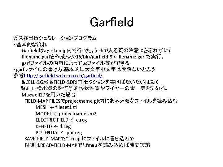
Maxwell 2 D と Garfield の使い方
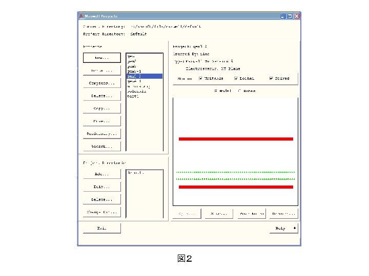
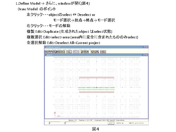
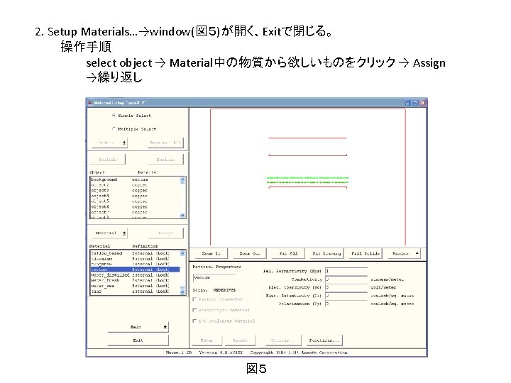
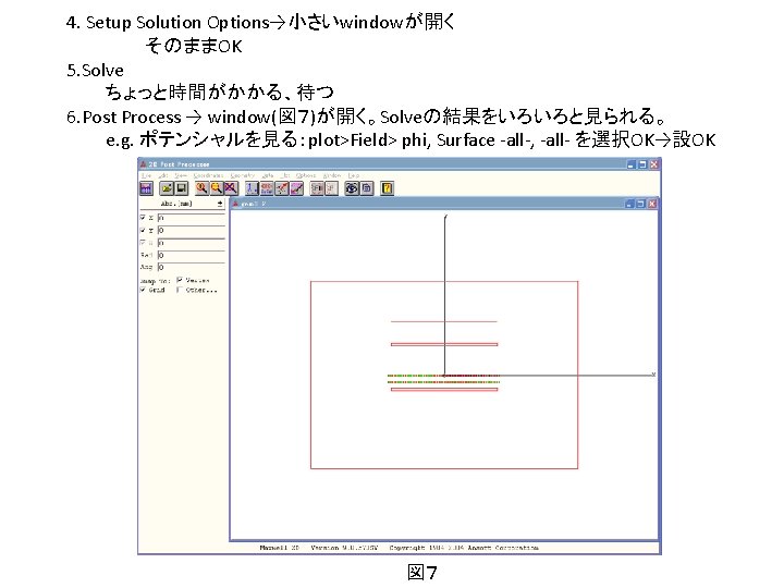
操作の流れ 1. Define Model 2. Setup Materials… 3. Setup Boundaries/ Sources… 4. Setup Solutions Options… 5. Solve 6. Post Process… 図3
3. Setup Boundaries/Sources → window(図6)が開く 操作手順 Sourceにしたいobject or 辺を選択→ voltage に値を入力→ Assign →繰り返し 図6
Garfieldのために 1. Post Process… において(図8) Data>Calculator を開く Qty>phi → Write> filename phi. reg →Clear → E, Dも同様にファイル作成 2. ファイル操作 Maxwell>defaultに ある projectname. pjt デ ィレクトリーを丸ご と Garfieldファイルの あるディレクトリー にコピーで Maxwell 2 D 終了 Garfieldへ 図8
GEMシュミレーション Maxwell 2 Dで作った 図8のモデルによる Garfieldでのシュミレーションを行った GEM(緑の部分) Pitch 0. 7 mm Drilled Hole diameter 0. 3 mm Etched Cu diameter 0. 5 mm Thickness of Cu 25μm Thickness of G 10 400μm -3600 V 11 mm -3000 V -2400 V -1800 V -600 V 2 mm 図8
potential &FIELD � area -0. 11 plot cont V range -4000. 0 -2000. 0 n=40 label area -0. 5 plot cont V range -4000. 0 n=40 label
Vector of Electric field &FIELD area -0. 11 grid 50 plot vector area -0. 5 grid 50 plot vector
Electric flux line &DRIFT area -0. 11 Call plot_drift_area Global bin 100 for i from 1 to bin do Global xmin -0. 11 Global xmax 0. 11 Global y=0. 1 Global track={xmin+(xmax-xmin)/bin*I} Call drift_electron_3(track, y, 0. 0) enddo Call plot_end 不均一なのがわかる。Maxwellのメッシュが大きいのか?
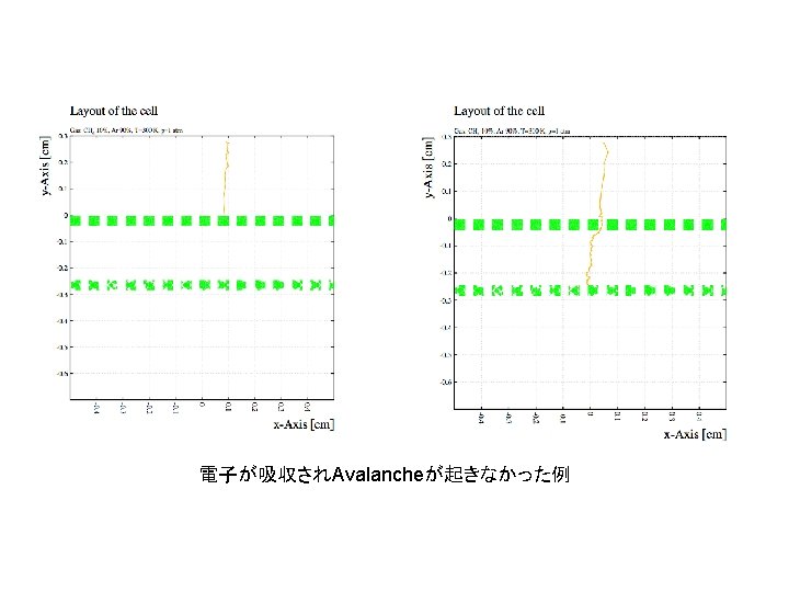
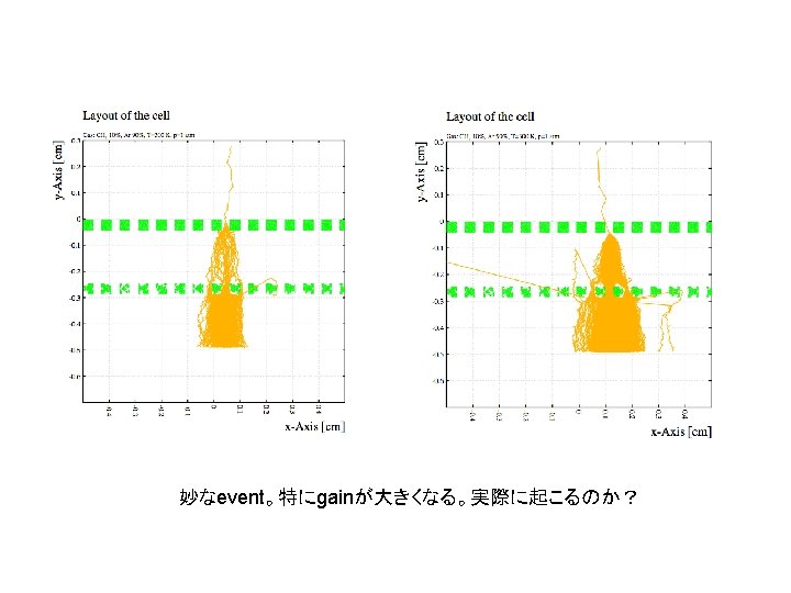
Event pattern of avalanche &DRIFT p. Int-par rojected-path-integration m-c-dist-int 0. 0002 m-c-coll 500 area -0. 5 -0. 7. 0. 5 0. 3 Call plot_drift_area Call avalanche( 0. 1, 0. 28, 0. 0, `plot-electron`) Call plot_end
Event pattern of avalanche Avalancheを起こした例
Call book_histogram(end_e, 100, -0. 7, 0. 3) avalanche(…, `y_e`, end_e, …) Call hplot (end_e, `y [cm]`, `End point of electron) Call plot_end avalanche 50回における 電子の止まった場所の数 この設定だと増幅した電子の 約1/3がGEM2に吸収される。 2 Dなので3 Dでどれくらい の値が出るかは不明 Read out GEM 2 GEM 1