Manipulating Atoms and Molecules Moving atoms with the
- Slides: 10

Manipulating Atoms and Molecules • Moving atoms with the STM • Unwinding proteins with an AFM • Using an AFM tip as pen

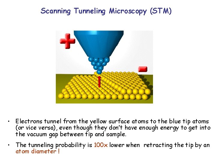
Scanning Tunneling Microscopy (STM) • Electrons tunnel from the yellow surface atoms to the blue tip atoms (or vice versa), even though they don’t have enough energy to get into the vacuum gap between tip and sample. • The tunneling probability is 100 x lower when retracting the tip by an atom diameter !

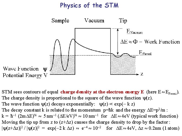
Physics of the STM sees contours of equal charge density at the electron energy E (here E EFermi). The charge density is proportional to the square of the wave function (z). The wave function (z) decays exponentially: (z) exp( k z) The decay constant k is related to the momentum p=ћk and the energy ΔE=p 2/m : k = ћ 1 (2 mΔE)½ 5 nm 1 (ΔE/e. V)½ 10 nm 1 for ΔE 4 e. V (typical work function) Moving the tip up from z to (z+ z) causes the charge density to drop by the factor : | (z+ z)|2 / | (z)|2 = exp( 2 k Δz) e 4 10 2 for ΔE 4 e. V, Δz 0. 2 nm (1 atom)

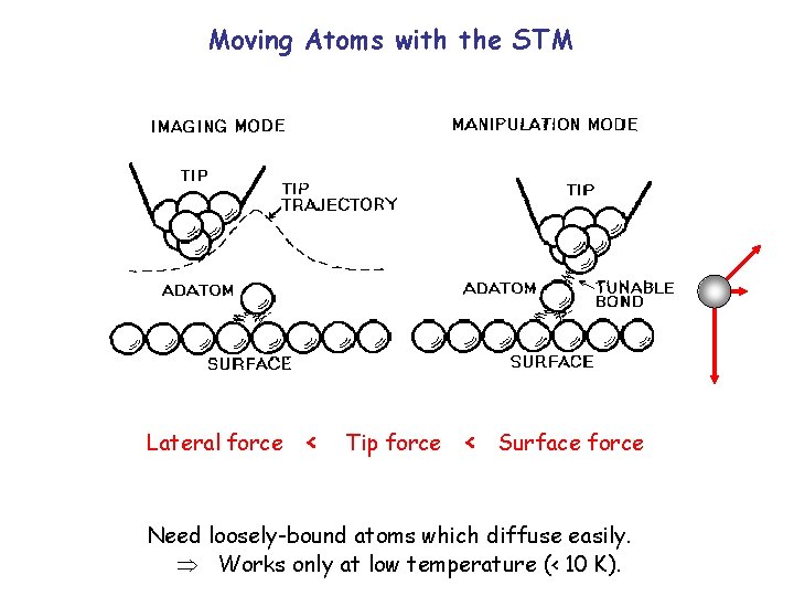
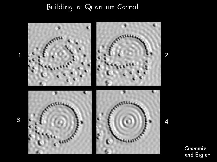
Moving Atoms with the STM Lateral force < Tip force < Surface force Need loosely-bound atoms which diffuse easily. Works only at low temperature (< 10 K).

Building a Quantum Corral 1 2 3 4 Crommie and Eigler

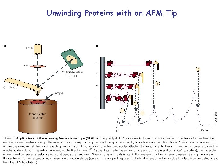
Unwinding Proteins with an AFM Tip

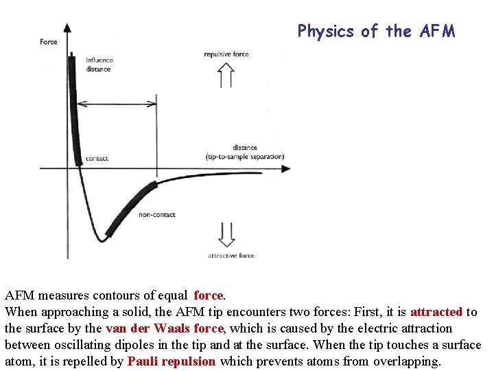
Physics of the AFM measures contours of equal force. When approaching a solid, the AFM tip encounters two forces: First, it is attracted to the surface by the van der Waals force, which is caused by the electric attraction between oscillating dipoles in the tip and at the surface. When the tip touches a surface atom, it is repelled by Pauli repulsion which prevents atoms from overlapping.

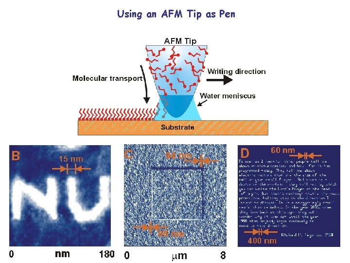
Using an AFM Tip as Pen

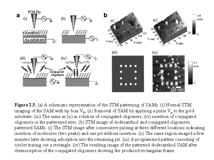
Figure 2. 5. (a) A schematic representation of the STM patterning of SAMs. (i) Normal STM imaging of the SAM with tip bias Vb; (ii) Removal of SAM by applying a pulse Vp to the gold substrate; (iii) The same as (ii) in solution of conjugated oligomers; (iv) insertion of conjugated oligomers in the patterened sites. (b) STM image of dodecanthiol and conjugated oligomeric patterned SAMs. (i) The STM image after consecutive pulsing at three different locations indicating insertion of molecules (two peaks) and one pit without insertion. (ii) The same region imaged a few minutes later showing adsorption into the remaining pit. (iii) A programmed pattern consisting of circles tracing out a rectangle. (iv) The resulting image of the patterned dodecanthiol SAM after chemisorption of the conjugated oligomers showing the produced rectangular frame.

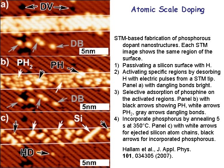
Atomic Scale Doping STM-based fabrication of phosphorous dopant nanostructures. Each STM image shows the same region of the surface. 1) Passivating a silicon surface with H. 2) Activating specific regions by desorbing H with electric pulses from a STM tip. Panel a) with dangling bonds bright. 3) Selective adsorption of phosphine on the activated regions. Panel b) with black arrows showing PH, white arrows PH 2, gray arrows dangling bonds. 4) Incorporate phosphorus by annealing 5 s at 350°C. Panel c) with white arrows for ejected silicon atom chains, black arrows for incorporated phosphorous. Hallam et al. , J. Appl. Phys. 101, 034305 (2007).