Low Voltage Low Power constant gm Rail to

- Slides: 18

Low Voltage Low Power constant - gm Rail to Rail CMOS Op-Amp with Overlapped Transition Regions ECEN 5007 9/3/02 Vishwas Ganesan

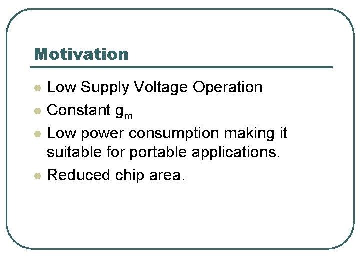
Motivation l l Low Supply Voltage Operation Constant gm Low power consumption making it suitable for portable applications. Reduced chip area.

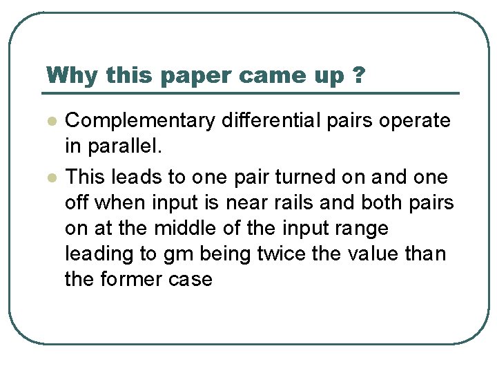
Why this paper came up ? l l Complementary differential pairs operate in parallel. This leads to one pair turned on and one off when input is near rails and both pairs on at the middle of the input range leading to gm being twice the value than the former case

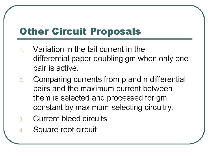
Other Circuit Proposals 1. 2. 3. 4. Variation in the tail current in the differential paper doubling gm when only one pair is active. Comparing currents from p and n differential pairs and the maximum current between them is selected and processed for gm constant by maximum-selecting circuitry. Current bleed circuits Square root circuit

Difficulties with other circuits l l l Increase in slew rate due to increase in tail current. Extra circuitry – Signal processing circuits and many more current mirrors. All this leads to complication, Power consumption and more die.

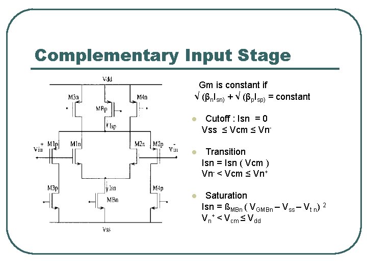
Complementary Input Stage Gm is constant if √ (βn. Isn) + √ (βp. Isp) = constant l Cutoff : Isn = 0 Vss ≤ Vcm ≤ Vn- l Transition Isn = Isn ( Vcm ) Vn- < Vcm ≤ Vn+ l Saturation Isn = ßMBn ( VGMBn – Vss – Vt n) 2 Vn+ < Vcm ≤ Vdd

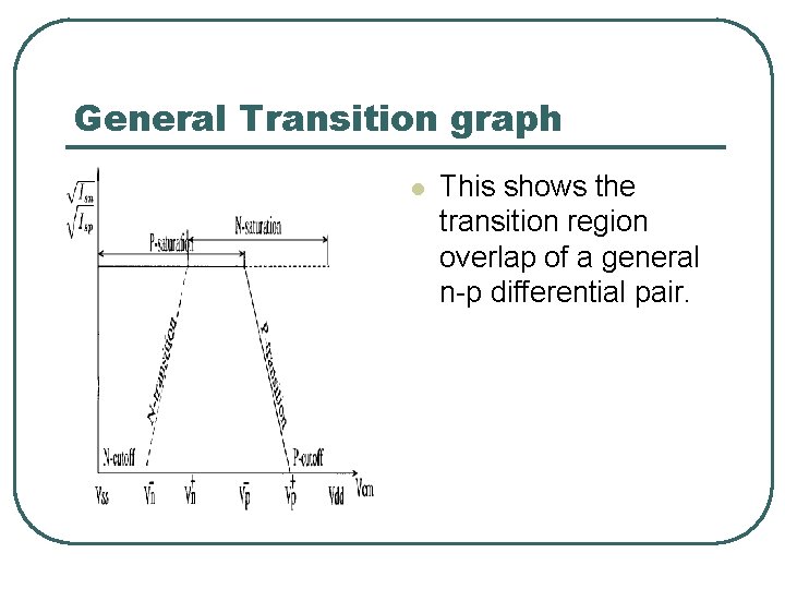
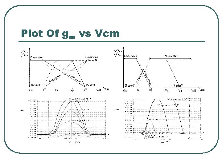
General Transition graph l This shows the transition region overlap of a general n-p differential pair.

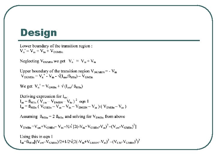
Design

Design

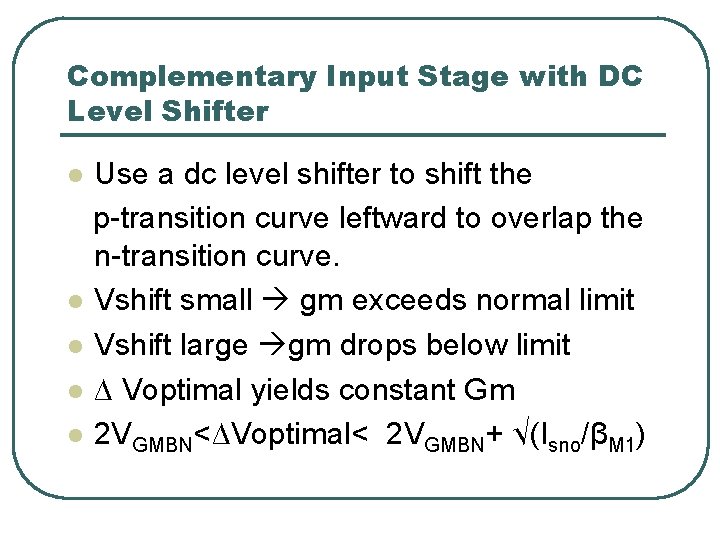
Complementary Input Stage with DC Level Shifter Use a dc level shifter to shift the p-transition curve leftward to overlap the n-transition curve. l Vshift small gm exceeds normal limit l Vshift large gm drops below limit l ∆ Voptimal yields constant Gm l 2 VGMBN<∆Voptimal< 2 VGMBN+ √(Isno/βM 1) l

Plot Of gm vs Vcm

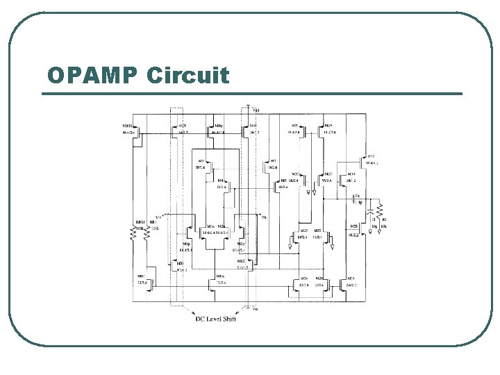
OPAMP Circuit

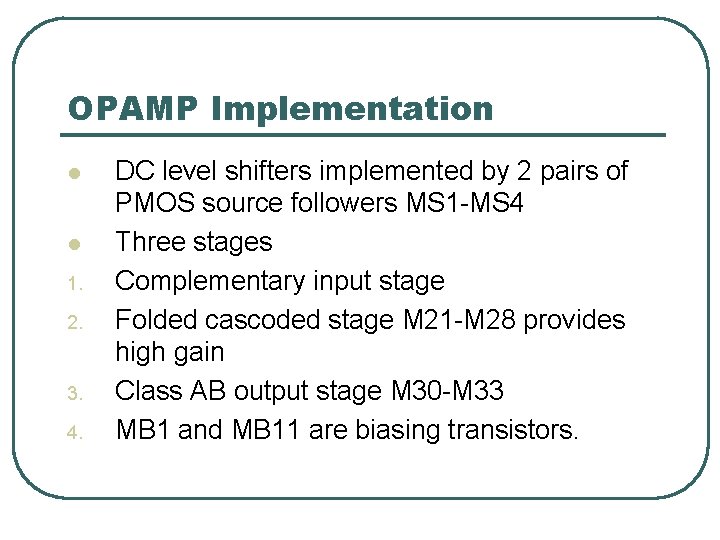
OPAMP Implementation l l 1. 2. 3. 4. DC level shifters implemented by 2 pairs of PMOS source followers MS 1 -MS 4 Three stages Complementary input stage Folded cascoded stage M 21 -M 28 provides high gain Class AB output stage M 30 -M 33 MB 1 and MB 11 are biasing transistors.

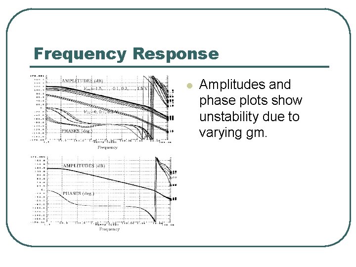
Frequency Response l Amplitudes and phase plots show unstability due to varying gm.

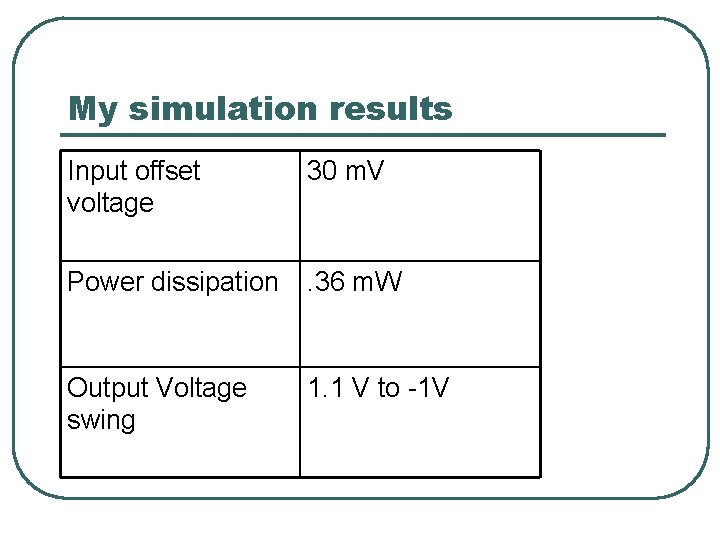
My simulation results Input offset voltage 30 m. V Power dissipation . 36 m. W Output Voltage swing 1. 1 V to -1 V

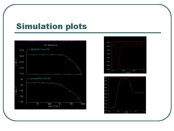
Simulation plots

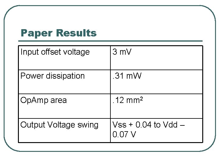
Paper Results Input offset voltage 3 m. V Power dissipation . 31 m. W Op. Amp area . 12 mm 2 Output Voltage swing Vss + 0. 04 to Vdd – 0. 07 V

Conclusions l l DC level shifters can be used to overlap transition regions to obtain constant gm. Low Power dissipation was achieved Low supply voltages. There is considerable gain achieved leading to CMRR improvement.