Low SEY LASE and NEG coated surfaces and
![Calculated and measured RS at frequency f=7. 8 GHz Sample Scan speed [mm/s] Groove Calculated and measured RS at frequency f=7. 8 GHz Sample Scan speed [mm/s] Groove](https://slidetodoc.com/presentation_image_h/209d82be6954a896bf02508d83bda4ec/image-10.jpg)
- Slides: 26

Low SEY LASE and NEG coated surfaces and their surface resistance and vacuum properties O. B. Malyshev and R. Valizadeh, on behalf of working team ASTe. C Vacuum Science Group, STFC Daresbury Laboratory, UK ECLOUD’ 18, Isola d'Elba, Italy, 3 -6 June 2018

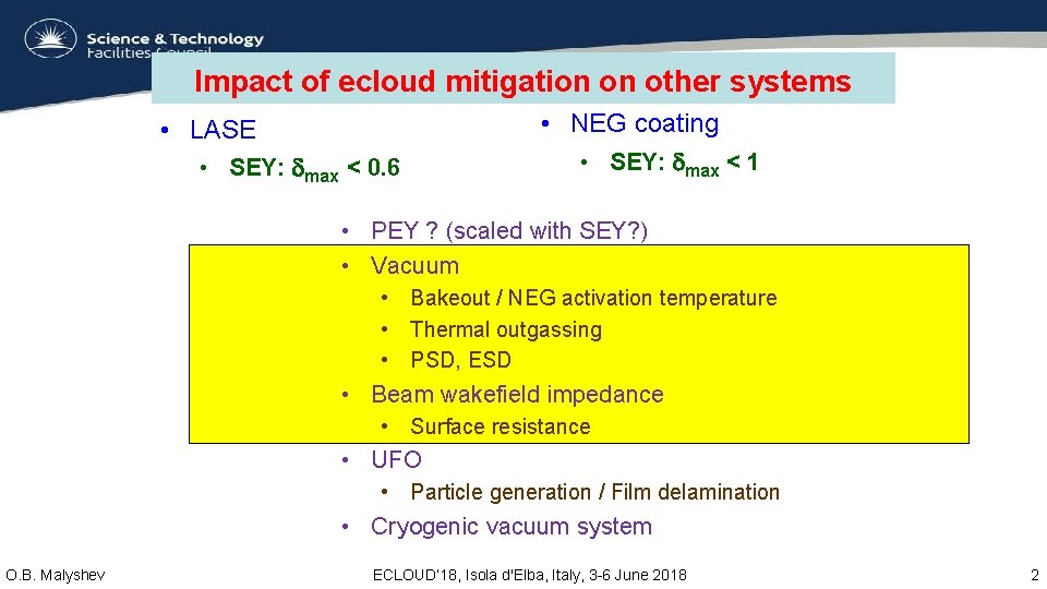
Impact of ecloud mitigation on other systems • LASE • SEY: max < 0. 6 • NEG coating • SEY: max < 1 • PEY ? (scaled with SEY? ) • Vacuum • Bakeout / NEG activation temperature • Thermal outgassing • PSD, ESD • Beam wakefield impedance • Surface resistance • UFO • Particle generation / Film delamination • Cryogenic vacuum system O. B. Malyshev ECLOUD’ 18, Isola d'Elba, Italy, 3 -6 June 2018 2

Surface resistance

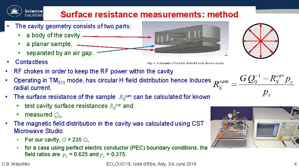
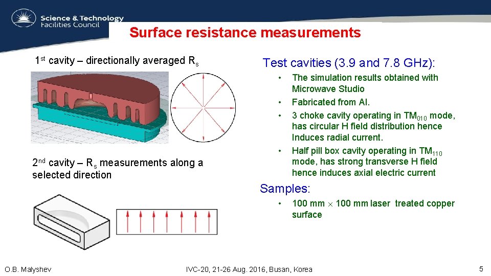
Surface resistance measurements: method • The cavity geometry consists of two parts: • a body of the cavity • a planar sample, • separated by an air gap. • Contactless • RF chokes in order to keep the RF power within the cavity • Operating in TM 010 mode, has circular H field distribution hence Induces radial current. • The surface resistance of the sample RSsam can be calculated for known • test cavity surface resistances RScav and • measured Q 0, • The magnetic field distribution in the cavity was calculated using CST Microwave Studio. • • For our cavity, G = 235 , for a case using perfect electric conductor (PEC) boundary conditions, the field ratios are pc = 0. 625 and ps = 0. 375. O. B. Malyshev ECLOUD’ 18, Isola d'Elba, Italy, 3 -6 June 2018 4

Surface resistance measurements 1 st cavity – directionally averaged Rs Test cavities (3. 9 and 7. 8 GHz): • • 2 nd cavity – Rs measurements along a selected direction The simulation results obtained with Microwave Studio Fabricated from Al. 3 choke cavity operating in TM 010 mode, has circular H field distribution hence Induces radial current. Half pill box cavity operating in TM 110 mode, has strong transverse H field hence induces axial electric current Samples: • O. B. Malyshev 100 mm laser treated copper surface IVC-20, 21 -26 Aug. 2016, Busan, Korea 5

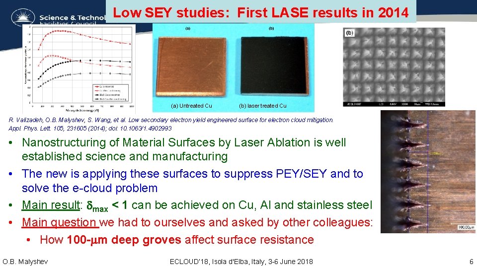
Low SEY studies: First LASE results in 2014 (a) Untreated Cu (b) laser treated Cu R. Valizadeh, O. B. Malyshev, S. Wang, et al. Low secondary electron yield engineered surface for electron cloud mitigation. Appl. Phys. Lett. 105, 231605 (2014); doi: 10. 1063/1. 4902993 • Nanostructuring of Material Surfaces by Laser Ablation is well established science and manufacturing • The new is applying these surfaces to suppress PEY/SEY and to solve the e-cloud problem • Main result: max < 1 can be achieved on Cu, Al and stainless steel • Main question we had to ourselves and asked by other colleagues: • How 100 - m deep groves affect surface resistance O. B. Malyshev ECLOUD’ 18, Isola d'Elba, Italy, 3 -6 June 2018 6

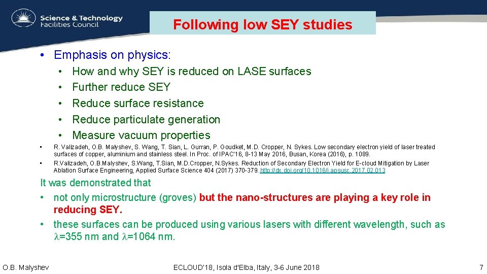
Following low SEY studies • Emphasis on physics: • • How and why SEY is reduced on LASE surfaces Further reduce SEY Reduce surface resistance Reduce particulate generation Measure vacuum properties R. Valizadeh, O. B. Malyshev, S. Wang, T. Sian, L. Gurran, P. Goudket, M. D. Cropper, N. Sykes. Low secondary electron yield of laser treated surfaces of copper, aluminium and stainless steel. In Proc. of IPAC’ 16, 8 -13 May 2016, Busan, Korea (2016), p. 1089. R. Valizadeh, O. B. Malyshev, S. Wang, T. Sian, M. D. Cropper, N. Sykes. Reduction of Secondary Electron Yield for E-cloud Mitigation by Laser Ablation Surface Engineering, Applied Surface Science 404 (2017) 370 -379. http: //dx. doi. org/10. 1016/j. apsusc. 2017. 02. 013 It was demonstrated that • not only microstructure (groves) but the nano-structures are playing a key role in reducing SEY. • these surfaces can be produced using various lasers with different wavelength, such as =355 nm and =1064 nm. O. B. Malyshev ECLOUD’ 18, Isola d'Elba, Italy, 3 -6 June 2018 7

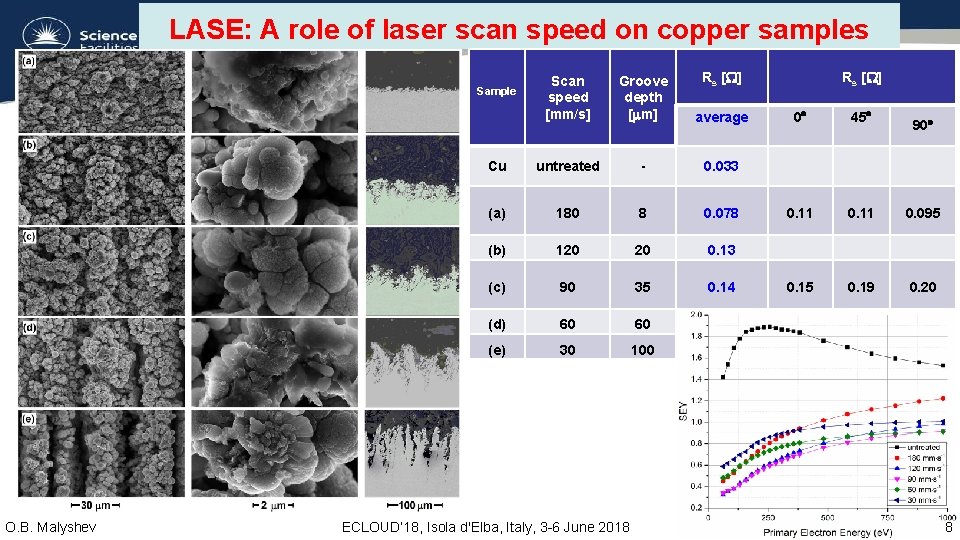
LASE: A role of laser scan speed on copper samples O. B. Malyshev Rs [ ] Scan speed [mm/s] Groove depth [ m] average Cu untreated - 0. 033 (a) 180 8 0. 078 (b) 120 20 0. 13 (c) 90 35 0. 14 (d) 60 60 (e) 30 100 Sample ECLOUD’ 18, Isola d'Elba, Italy, 3 -6 June 2018 Rs [ ] 0 45 0. 11 0. 095 0. 19 0. 20 90 8

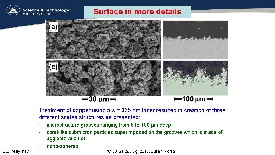
Surface in more details Treatment of copper using a λ = 355 nm laser resulted in creation of three different scales structures as presented: • • • O. B. Malyshev microstructure grooves ranging from 8 to 100 µm deep, coral-like submicron particles superimposed on the grooves which is made of agglomeration of nano-spheres IVC-20, 21 -26 Aug. 2016, Busan, Korea 9
![Calculated and measured RS at frequency f7 8 GHz Sample Scan speed mms Groove Calculated and measured RS at frequency f=7. 8 GHz Sample Scan speed [mm/s] Groove](https://slidetodoc.com/presentation_image_h/209d82be6954a896bf02508d83bda4ec/image-10.jpg)
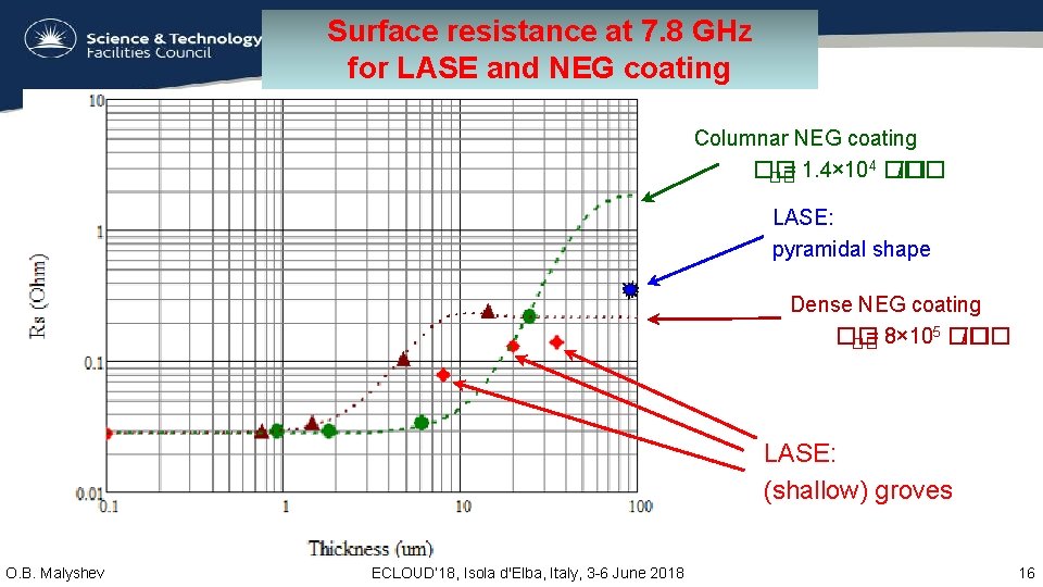
Calculated and measured RS at frequency f=7. 8 GHz Sample Scan speed [mm/s] Groove depth for LASE (Roughness for untreated metals) [ m] Rs [ ] measured with a 7. 8 -GHz cavity Rs [ ] calc with formula Cu untreated 0. 4 0. 028 0. 029 (a) 180 8 0. 078 0. 046 (b) 120 20 0. 13 0. 046 (c) 90 35 0. 14 0. 046 (d) 60 60 0. 046 (e) 30 100 0. 046 Al untreated 0. 4 0. 034 Nb untreated 1. 0 0. 071 0. 080 SS untreated 1. 4 0. 17 0. 16 Hammerstad and Bekkadal formula: O. B. Malyshev ECLOUD’ 18, Isola d'Elba, Italy, 3 -6 June 2018 10

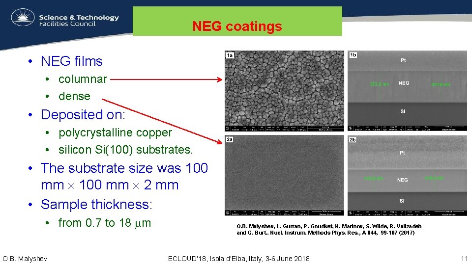
NEG coatings • NEG films • columnar • dense • Deposited on: • polycrystalline copper • silicon Si(100) substrates. • The substrate size was 100 mm 2 mm • Sample thickness: • from 0. 7 to 18 m O. B. Malyshev, L. Gurran, P. Goudket, K. Marinov, S. Wilde, R. Valizadeh and G. Burt. . Nucl. Instrum. Methods Phys. Res. , A 844, 99 -107 (2017) ECLOUD’ 18, Isola d'Elba, Italy, 3 -6 June 2018 11

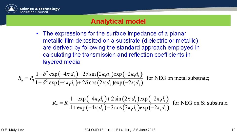
Analytical model • The expressions for the surface impedance of a planar metallic film deposited on a substrate (dielectric or metallic) are derived by following the standard approach employed in calculating the transmission and reflection coefficients in layered media O. B. Malyshev ECLOUD’ 18, Isola d'Elba, Italy, 3 -6 June 2018 12

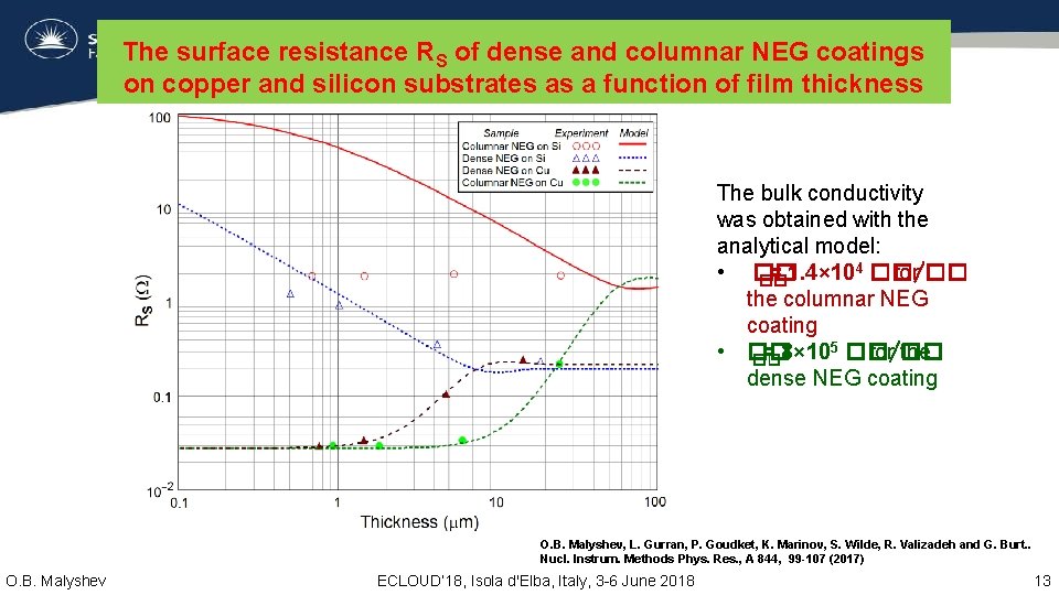
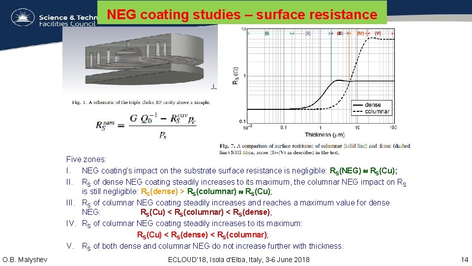
The surface resistance RS of dense and columnar NEG coatings on copper and silicon substrates as a function of film thickness The bulk conductivity was obtained with the analytical model: • �� = 1. 4× 10⁴ ��/�� for �� the columnar NEG coating • �� = 8× 10⁵ ��/�� for the �� dense NEG coating O. B. Malyshev, L. Gurran, P. Goudket, K. Marinov, S. Wilde, R. Valizadeh and G. Burt. . Nucl. Instrum. Methods Phys. Res. , A 844, 99 -107 (2017) O. B. Malyshev ECLOUD’ 18, Isola d'Elba, Italy, 3 -6 June 2018 13

NEG coating studies – surface resistance Five zones: I. NEG coating’s impact on the substrate surface resistance is negligible: RS(NEG) RS(Cu); II. RS of dense NEG coating steadily increases to its maximum, the columnar NEG impact on RS is still negligible: RS(dense) > RS(columnar) RS(Cu); III. RS of columnar NEG coating steadily increases and reaches a maximum value for dense NEG: RS(Cu) < RS(columnar) < RS(dense); IV. RS of columnar NEG coating steadily increases to its maximum: RS(Cu) < RS(dense) < RS(columnar); V. RS of both dense and columnar NEG do not increase further with thickness. O. B. Malyshev ECLOUD’ 18, Isola d'Elba, Italy, 3 -6 June 2018 14

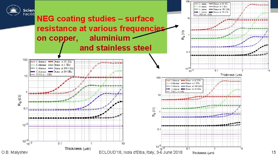
NEG coating studies – surface resistance at various frequencies on copper, aluminium and stainless steel O. B. Malyshev ECLOUD’ 18, Isola d'Elba, Italy, 3 -6 June 2018 15

Surface resistance at 7. 8 GHz for LASE and NEG coating Columnar NEG coating �� = 1. 4× 10⁴ �� /�� �� LASE: pyramidal shape Dense NEG coating �� = 8× 10⁵ �� /�� �� LASE: (shallow) groves O. B. Malyshev ECLOUD’ 18, Isola d'Elba, Italy, 3 -6 June 2018 16

Surface resistance • An open question: • Rs as a function of temperature • To be addressed in future • A dedicated facility in ASTe. C is under development • Planar samples could be studied in a few months • Tubular sample can be considered later O. B. Malyshev ECLOUD’ 18, Isola d'Elba, Italy, 3 -6 June 2018 17

Vacuum properties

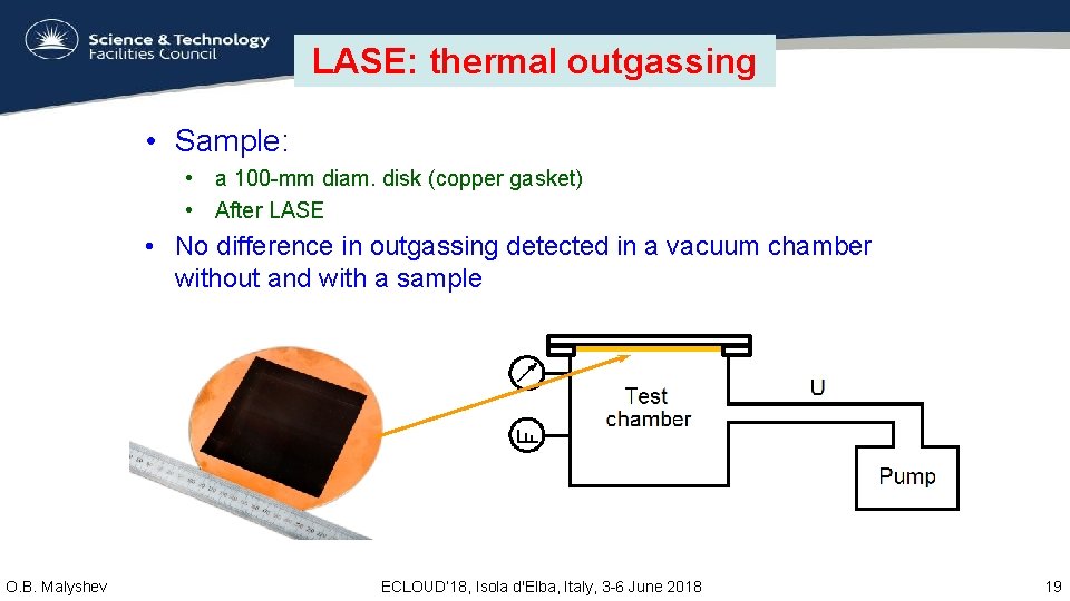
LASE: thermal outgassing • Sample: • a 100 -mm diam. disk (copper gasket) • After LASE • No difference in outgassing detected in a vacuum chamber without and with a sample O. B. Malyshev ECLOUD’ 18, Isola d'Elba, Italy, 3 -6 June 2018 19

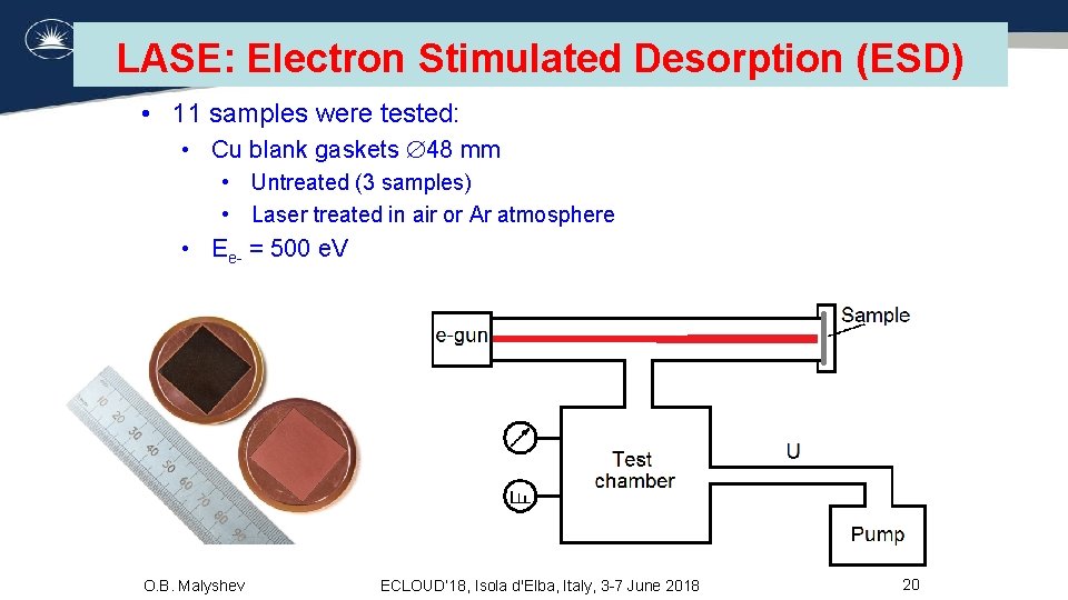
LASE: Electron Stimulated Desorption (ESD) • 11 samples were tested: • Cu blank gaskets 48 mm • Untreated (3 samples) • Laser treated in air or Ar atmosphere • Ee- = 500 e. V O. B. Malyshev ECLOUD’ 18, Isola d'Elba, Italy, 3 -7 June 2018 20

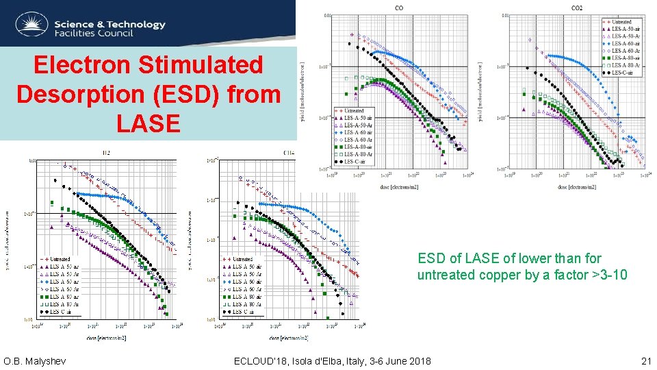
Electron Stimulated Desorption (ESD) from LASE ESD of LASE of lower than for untreated copper by a factor >3 -10 O. B. Malyshev ECLOUD’ 18, Isola d'Elba, Italy, 3 -6 June 2018 21

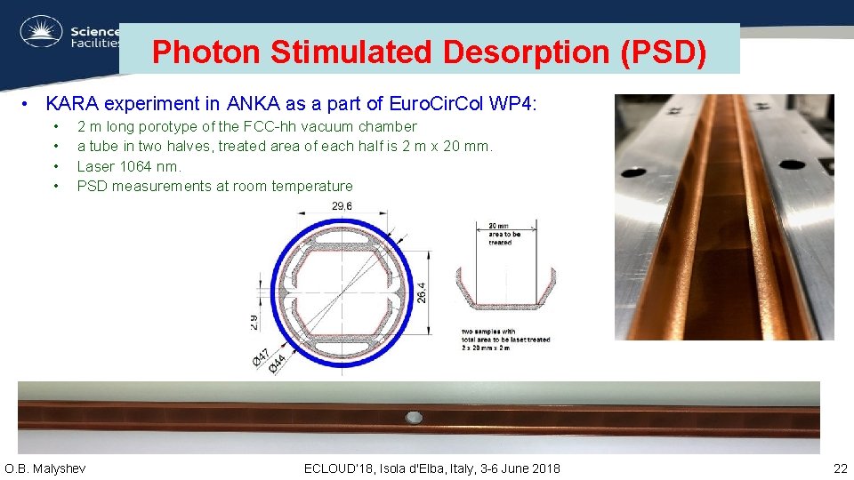
Photon Stimulated Desorption (PSD) • KARA experiment in ANKA as a part of Euro. Cir. Col WP 4: • • 2 m long porotype of the FCC-hh vacuum chamber a tube in two halves, treated area of each half is 2 m x 20 mm. Laser 1064 nm. PSD measurements at room temperature O. B. Malyshev ECLOUD’ 18, Isola d'Elba, Italy, 3 -6 June 2018 22

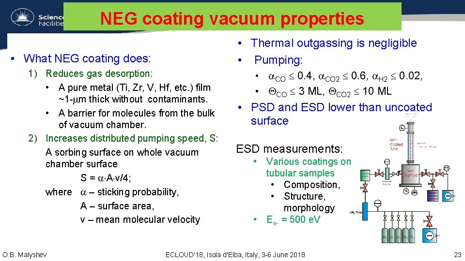
NEG coating vacuum properties • Thermal outgassing is negligible • Pumping: • What NEG coating does: 1) Reduces gas desorption: • A pure metal (Ti, Zr, V, Hf, etc. ) film ~1 - m thick without contaminants. • A barrier for molecules from the bulk of vacuum chamber. 2) Increases distributed pumping speed, S: A sorbing surface on whole vacuum chamber surface S = A v/4; where – sticking probability, A – surface area, v – mean molecular velocity O. B. Malyshev • CO 0. 4, CO 2 0. 6, H 2 0. 02, • CO 3 ML, CO 2 10 ML • PSD and ESD lower than uncoated surface ESD measurements: • Various coatings on tubular samples • Composition, • Structure, morphology • Ee- = 500 e. V ECLOUD’ 18, Isola d'Elba, Italy, 3 -6 June 2018 23

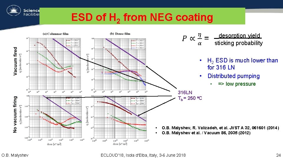
ESD of H 2 from NEG coating desorption yield sticking probability • H 2 ESD is much lower than for 316 LN • Distributed pumping • => low pressure 316 LN Tb = 250 C • • O. B. Malyshev, R. Valizadeh, et al. JVST A 32, 061601 (2014) O. B. Malyshev et al. / Vacuum 86, 2035 (2012) ECLOUD’ 18, Isola d'Elba, Italy, 3 -6 June 2018 24

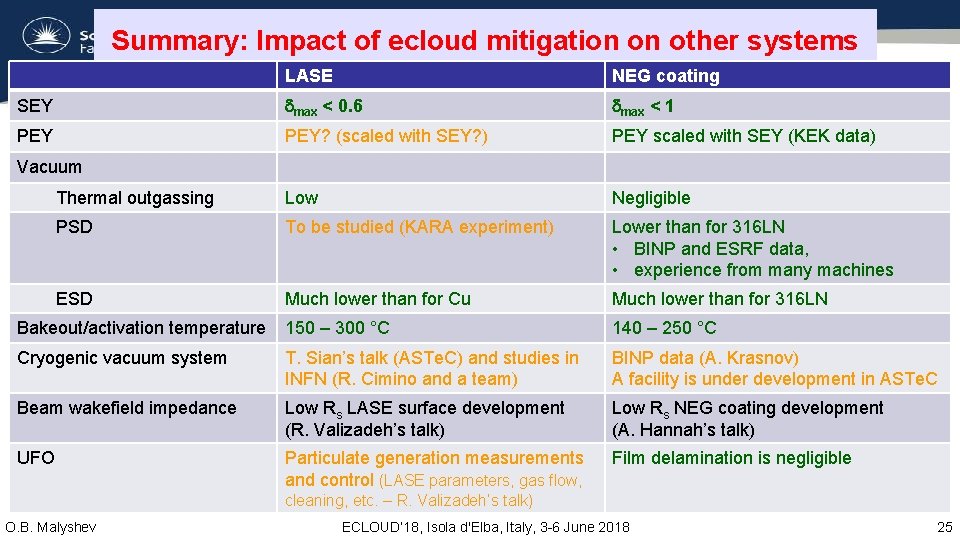
Summary: Impact of ecloud mitigation on other systems LASE NEG coating SEY max < 0. 6 max < 1 PEY? (scaled with SEY? ) PEY scaled with SEY (KEK data) Thermal outgassing Low Negligible PSD To be studied (KARA experiment) Lower than for 316 LN • BINP and ESRF data, • experience from many machines ESD Much lower than for Cu Much lower than for 316 LN Bakeout/activation temperature 150 – 300 °C 140 – 250 °C Cryogenic vacuum system T. Sian’s talk (ASTe. C) and studies in INFN (R. Cimino and a team) BINP data (A. Krasnov) A facility is under development in ASTe. C Beam wakefield impedance Low Rs LASE surface development (R. Valizadeh’s talk) Low Rs NEG coating development (A. Hannah’s talk) UFO Particulate generation measurements and control (LASE parameters, gas flow, Film delamination is negligible Vacuum cleaning, etc. – R. Valizadeh’s talk) O. B. Malyshev ECLOUD’ 18, Isola d'Elba, Italy, 3 -6 June 2018 25

Collaboration Team Dr Oleg Malyshev Dr Reza Valizadeh Adrian Hannah James Conlon Taaj Sian Ruta Sirvinskaite Dr Phillippe Goudket Dr Stuart Wilde Shrikant Pattlawar Ninad Pattlawar Dr Jonthan Smith (Tech X) Neil Sykes (Micronanics) Dr Greame Burt (Lancaster) Dr Vin Danak (Liverpool) Dr Karl Dawson (Liverpool) Dr Walter Perrie (Liverpool) Dr Mike Cropper (Loughborough) Dr David Whitehead (Manchester)