Integrated photonics to revolutionize the Data Center hardware


 Datacom (CXP, CPAK) Data center access")
 optical module to enable Terabit blades or line-cards The")


 @ 3 d. B bandwidth (GHz) 1550 nm")
 • Wavelength agnostic: works across all")


- Slides: 23
Integrated photonics to revolutionize the Data Center hardware Marco Romagnoli CNIT & Te. CIP - Scuola Superiore Sant’Anna
Zettabyte era • • • Disaggregation at system level Integration at chip level Optical interconnection at shorter reach Electronics-photonics convergence Cost, energy and bandwidth density Architecture, components, programming Make it happen or end the information age
Example of large volume applications • Active Optical Cable • Wireless communications • 100 GE Optical Interfaces (CFP, CXP, CPAK, QFSP, . . ) • Inter Chip and Board Level Interconnection
Optical Interfaces for Different Network Platforms Telecom (CFP) Datacom (CXP, CPAK) Data center access Data center aggregation Edge routing The Optical challenges: Bandwidth Density Consumption Cost Core routing
The CFP (C Form-Factor Pluggable) optical module to enable Terabit blades or line-cards The next-generation CFP modules - the CFP 2 and CFP 4 (10/40 km) multiplies the number of 100 Gb/s optical module interfaces on a blade. Using the CFP 4, up to 16, 100 Gbps modules will fit on a blade, a total line rate of 1. 6 Tb/s. With a goal of a 60 W total module power budget per blade, that equates to 27 Gb/s/W. In comparison, the power-efficient SFP+ achieves 10 Gbps/W.
Inter Chip and Board Level Interconnection Case study: «Optical PCIe 3. 0» working group within the Communication Technology Roadmap (CTR 4) of the Microphotonics Center Consortium (MPh. C) at MIT
Chip to Memory Interconnection through Si interposer
Technology • Photonic Electronic Integration • Silicon Optical Interposer • Si Photonics readiness • Laser Integration
Si Photonics - Advantage of full integration Cost: photonic-electronic chip (development, mask set, wafers, manufacturing). Save in packaging, wire bonding and traces/pin-out. Technology: low capacitance 3 D integration. Node scalability, low consumption and improved yield. Performances: trade off between consumption, size, IL and link/system specs Maturity of individual components: to be improved but not conceptually limited. 50 line Photonic chip 9
Photonic Electronic Layer - 3 D Integration 3 D integration of SOI technology for the photonic layers with Si CMOS circuit layers. Integration in a 65 nm node/12” fab based on wf/wf or wf/die bonding and low capacitance TSV technology. Bond Pads Si Logic Layer Si TSV Thermal Compression Bonding Mod PD BOX SOI Photonics Layer Si waveguide Substrate 10
Electrical Interconnect Limitations • • Bandwidth Limitations – Wires are not scalable i. e. bandwidth is limited by area Power Limitations - Total interconnect power is high ~50% of Total Chip Power Expected to rise to >80% (limit 200 W). • • • Signal Integrity and Latency (RC delay) will increase considerably with scaling, sheet Resistance and Capacitance increase as RC = Rsheet. Csheet/� 2 Xtalk between metal wires requires a minimum pitch that limitates interconnection density Repeaters in electrical lines increase delay Al/Oxide + Gates Cwire= 2 p. F/cm Rwire= 20 /cm Al/Oxide Sam Naftziger, AMD fellow 2011 VLSI Symposium Keynote Cu + Gate Cu Gate
Optical Interconnect and Switching • • Optical links are distance and power independent BW density can increase by wavelength multiplexing Latency is given by propagation distance (5 ps/mm) Optical switching Reconfigurable Optical Add Drop Multiplexer CNIT/Ericsson OFC 2014
Si Interposer and Si Optical Interposer Si Interposer Metal Pad / via 100 nm P + Si Optical Interposer Coupler Optical Fiber I/O Silica Waveguides 480 nm 220 nm P N Oxide N + N P MZI Modulato Si r Substrate Heat Sink Micro Bumps HMC P + BOX Interposer Package Redistribution layer Flip Chip Bumps BGA Balls Interpose / Photonics Layer TSV 1. 5 um Silicon Waveguides, resonators, detectors HMC ASIC PG + e N Silicon + Waveguide Ge Photodetect or Redistribution Layer
Si Photonics Modulators Parameter/device type MZI Microring MZI MOSCAP FK Ge EAM Hybrid In. P/Si MZI Bandwidth (nm) >20 0. 1 >100 20 100 Temp Sensitivity (GHz/K) NA 3 ÷ 10 NA NA ? Energy Cost (f. J/bit) 5 ÷ 30 x 103 7 ÷ 50 * 500** 50 ÷ 100 8000 (state switching) Footprint (µm 2) 200 ÷ 10000 20 ÷ 100 500 x 5 25 250 ÷ 500 Speed (GHz) 30 25 10*** 30 25 Insertion Loss (d. B) Extintion Ratio (d. B) 7 7 15 3 ÷ 4 4 1 @ 30 Gb/s 8 @ 16 Gb/s >10 4 ÷ 7. 5 10 @ 25 Gb/s, 18 static 6. 5 1 ÷ 2 1 4 1. 2 Phase adjustment 0. 2 nm/m. W (thermal) Phase adjustment Voltage Static Tuning * add 100 f. J/bit for thermal trimming ** 1 p. J/bit including driver *** progressing towards 40 Gb/s
Si Photonics: Accumulation Modulator
Si Photonics: Detector Integration Responsivity (A/W) @ 3 d. B bandwidth (GHz) 1550 nm Dark Current Device Density (μA) @ -1 V Design Max 1. 0@-3 V 0 bias - Max 4. 5@-3 V 0 bias - (m. A/cm 2) 0. 7* 2× 10 -4 1. 08 7. 2 6. 6 1. 3 x 103 * 1 1 0 25@-6 V - 6. 5 x 105 * 130 0. 89 31@-2 V 15. 7 51@2 V 0. 85 26 - 0. 65 - 18 Reference butt, p-i-n top, p-i-n butt, msm Liu 2006 Beals 2008 Ahn 2007 0. 17@-2 V bottom, p-i-n Yin 2007 - 3 bottom, p-i-n Masini 2008 - 125 0. 06 bottom p-i-n Wang 2008 1. 3 butt p-i-n butt, p-i-n bottom msm bottom, p-i-n bottom, JFET Feng 2009 1. 1 - 37@-3 V 17. 5 1. 6× 10⁴ 1@-4 V 0. 2 42@-4 V 12 60 0. 018 0. 42 0 40@-2. 5 V - - 90 0. 95 - 36 - 29 0. 0046 0. 64 - 8 - - 0. 5 Vivien 2007 Vivien 2009 Assefa 2010 Liao 2011 Wang 2011 J. Michel et al. , Nature Photonics, 4, 527 (2010) 16
ADN 3000 -06/11 Integrated Optical Receiver (Analog Devices) • Wavelength agnostic: works across all key optical wavelengths including 850 nm, 1310 nm and 1550 nm • No bonding wires • Single, fully-tested die solution reduces cost: No separate tests required for the TIA and PD • 65 -m. W power consumption: 50 percent powewr reduction compared to standard designs Differential Optical Pricing Each Data Rate Detector Size Output Modulation Per 1000 (Gbps) (um) Swing (m. V p Amplitude -p) (d. Bm) Power Dissipation (m. W) Product Sample Availability ADN 3000 -06 -50 Now $3. 95 6 50 240 -19 65 ADN 3000 -11 -35 Now $5. 95 11 35 240 -17 65 APPLICATIONS Optical receivers up to 10 Gbps 6 G CPRI, OBSAI, and 8 G short range and LTE receivers Receiver optical subassemblies (ROSA)
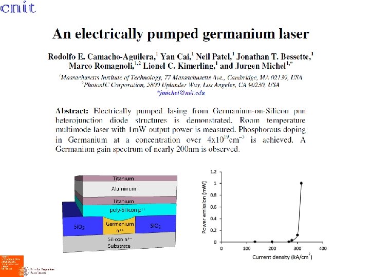
Si Photonics Full integration: Integrated Laser Source VCSEL: conventional solution for <100 m reach. Good for power consumption, temperature stability, packaging and cost. MM and SM version. High T operation. Hybrid mounting III-V Laser: conventional solution. It can be butt coupled or coupled through grating coupler. Coupling loss 1 ÷ 3 d. B, Packaging, assembly. Cost and large consumption. High T operation. Bonded III-V Laser: remarkable solution with a certain maturity. CMOS manufacturing to be demonstrated. High T operation. Quantum Dot Laser: It can be butt coupled or coupled through grating coupler. Coupling loss 1 ÷ 3 d. B, TEC, Packaging, assembly. Very high T operation. Ge Laser: early stage. Monolithic integration. Potential good performance (power and threshold). Large gain BW and wide tunability. Best at high T (80 ÷ 100°C). 18
Aurrion • Hybrid Silicon Platform bonds III/V wafer or die to silicon. 150 -mm wafer bonding and processing possible; • III/V processed in low-temperature backend process; • Mode couples to III/V optical gain, detection or modulation from III-V Material. Fujitsu • Hybrid III/V SOA mounted on Si Platforrm; • Mode butt couples to III/V optical gain Fujitsu
Quantum Dot Laser - In. As multi-stacked quantum dot active layers sandwitched by Ga. As/Al. Ga. As cladding layers on a 3 -inch Ga. As substrate - Leading-edge highly-uniform, and high-density quantum dots for high optical gain - Light emission wavelength of 1. 21 to 1. 29 μm at room temperature
Conclusion Assuming • Maturity of Si Photonics, good performance, component availability • Initial stage of photonics electronics integration Needs • Low consumption, uncooled operation laser integration evolution • Photonic Electronic convergence through Si optical interposer (3 D integration, TSV’s interconnections) Result • Huge energy saving • Latency control • Increased BW density • Miniaturization • Lower costs Zettabyte Era
thank you! email: marco. romagnoli@cnit. it