INEL 4207 DYNAMIC AND DOMINO LOGIC Dynamic Logic


- Slides: 14

INEL 4207 DYNAMIC AND DOMINO LOGIC

Dynamic Logic: Clocked Logic Design methodology in combinatory logic circuits, particularly those implemented in MOS technology. Temporary storage of information in stray and gate capacitances Two phases Precharge Evaluation Are faster than static logic and required less area, more difficult to design for

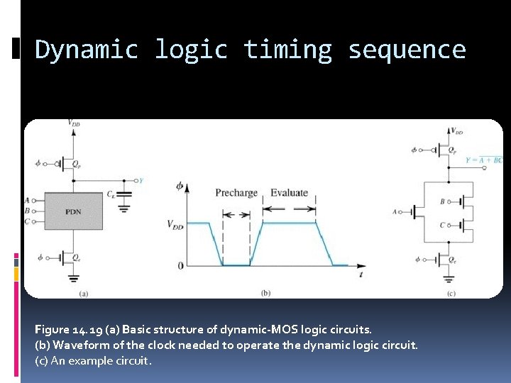
Dynamic logic timing sequence Figure 14. 19 (a) Basic structure of dynamic-MOS logic circuits. (b) Waveform of the clock needed to operate the dynamic logic circuit. (c) An example circuit.

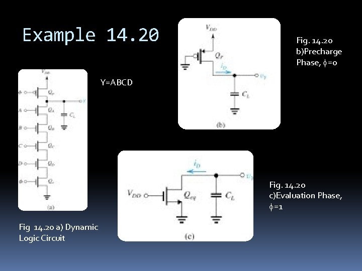
Example 14. 20 Fig. 14. 20 b)Precharge Phase, f=0 Y=ABCD Fig. 14. 20 c)Evaluation Phase, f=1 Fig 14. 20 a) Dynamic Logic Circuit

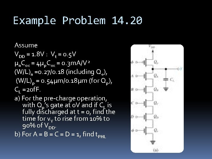
Example Problem 14. 20 Assume VDD = 1. 8 V : Vt = 0. 5 V μn. Cox = 4μp. Cox = 0. 3 m. A/V 2 (W/L)n =0. 27/0. 18 (including Qe), (W/L)p = 0. 54μm/0. 18μm (for Qp), CL =20 f. F. a) For the pre-charge operation, with Qp’s gate at 0 V and if CL is fully discharged at t = 0, find the time for v. Y to rise from 10% to 90% of VDD. b) For A = B = C = D = 1, find t. PHL

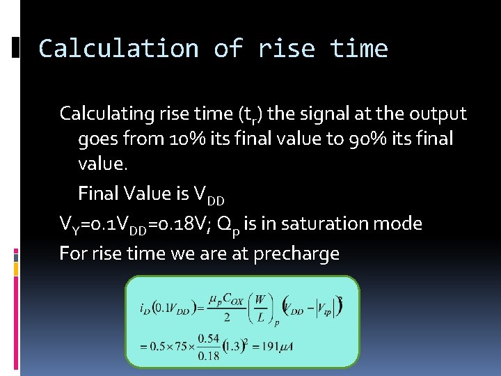
Calculation of rise time Calculating rise time (tr) the signal at the output goes from 10% its final value to 90% its final value. Final Value is VDD VY=0. 1 VDD=0. 18 V; Qp is in saturation mode For rise time we are at precharge

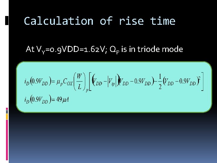
Calculation of rise time At VY=0. 9 VDD=1. 62 V; QP is in triode mode

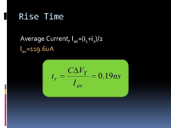
Rise Time Average Current, Iav=(i 1+i 2)/2 Iav=119. 6 u. A

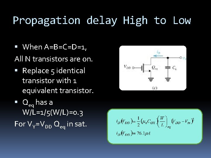
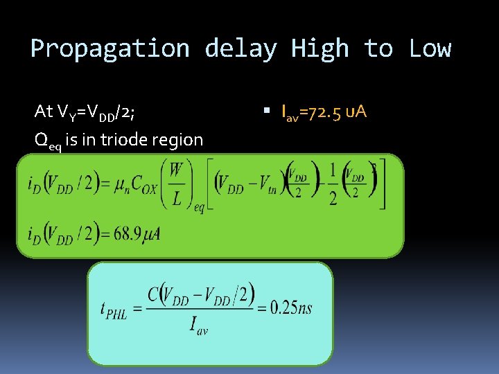
Propagation delay High to Low When A=B=C=D=1, All N transistors are on. Replace 5 identical transistor with 1 equivalent transistor. Qeq has a W/L=1/5(W/L)=0. 3 For VY=VDD Qeq in sat.

Propagation delay High to Low At VY=VDD/2; Qeq is in triode region Iav=72. 5 u. A

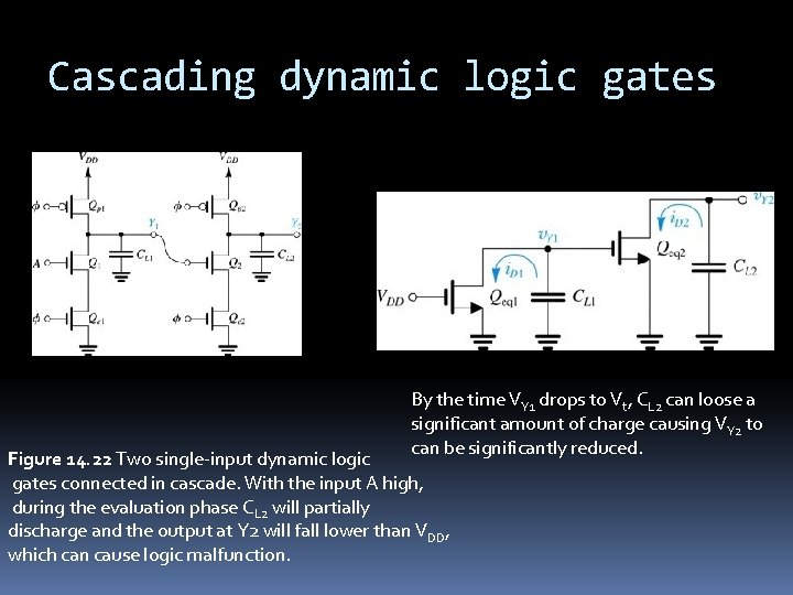
Cascading dynamic logic gates By the time VY 1 drops to Vt, CL 2 can loose a significant amount of charge causing VY 2 to can be significantly reduced. Figure 14. 22 Two single-input dynamic logic gates connected in cascade. With the input A high, during the evaluation phase CL 2 will partially discharge and the output at Y 2 will fall lower than VDD, which can cause logic malfunction.

Domino Logic A cascadable Dynamic Logic gate

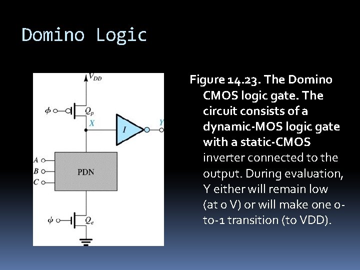
Domino Logic Figure 14. 23. The Domino CMOS logic gate. The circuit consists of a dynamic-MOS logic gate with a static-CMOS inverter connected to the output. During evaluation, Y either will remain low (at 0 V) or will make one 0 to-1 transition (to VDD).

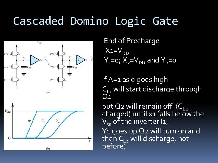
Cascaded Domino Logic Gate End of Precharge X 1=VDD Y 1=0; X 2=VDD and Y 2=0 If A=1 as f goes high CL 1 will start discharge through Q 1 but Q 2 will remain off (CL 2 charged) until x 1 falls below the Vtn of the inverter I 1, Y 1 goes up Q 2 will turn on and then CL 2 will discharge, not before)