High level modem development for Radio Link INF

- Slides: 17

High level modem development for Radio Link INF 3430/4431 H 2013 WORLD CLASS – through people, technology and dedication 1

Agenda § Project task § VHDL generation Tools § Overview of Radio Link and modem § Introduction to System Generator from Xilinx § Design § On-chip debug and verification § Experiences © KONGSBERG 26 August 2003 2

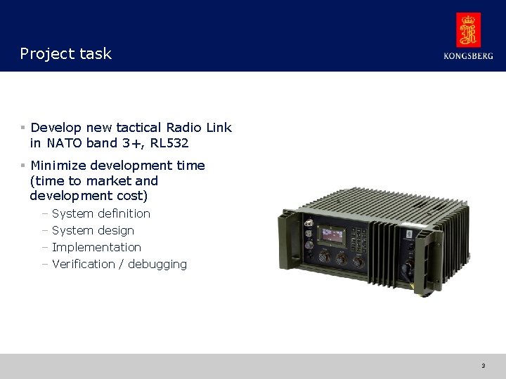
Project task § Develop new tactical Radio Link in NATO band 3+, RL 532 § Minimize development time (time to market and development cost) – System definition – System design – Implementation – Verification / debugging © KONGSBERG 26 August 2003 3

Why “High level” modem implementation § Motivation – Decrease development time relative to hand coded VHDL – Use DSP engineers for implementation (not only specification) § Earlier experiences with C based datapath implementation tools – DSP station DIRAC (MRR) – Art. Designer NOVA (LFR) © KONGSBERG 26 August 2003 4

Simulink based VHDL generators § Chip proprietary solutions Simulink based – System Generator, Xilinx - Accel DSP (m code), Xilinx – DSP Builder, Altera § Non proprietary solutions Simulink based – Simulink HDL coder, Matworks – Simplify DSP, Simplicity § Non proprietary solutions ANSI C++ code based – Catapult C, Mentor © KONGSBERG 26 August 2003 5

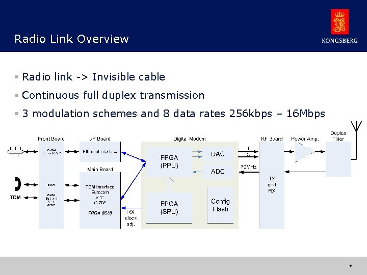
Radio Link Overview § Radio link -> Invisible cable § Continuous full duplex transmission § 3 modulation schemes and 8 data rates 256 kbps – 16 Mbps © KONGSBERG 26 August 2003 6

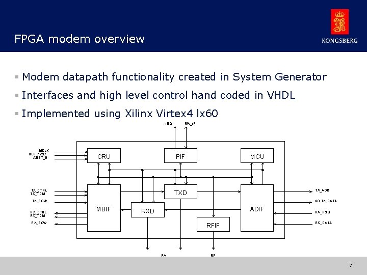
FPGA modem overview § Modem datapath functionality created in System Generator § Interfaces and high level control hand coded in VHDL § Implemented using Xilinx Virtex 4 lx 60 IRQ MCLK CLK_7 M 37 ARST_N CRU RW_IF PIF TX_CTRL TX_TDM MCU TX_AGC TXD TX_EOW RX_CTRL RX_TDM I/Q TX_DATA MBIF ADIF RXD RX_EOW RFIF PA © KONGSBERG 26 August 2003 RX_RSSI RX_DATA RF 7

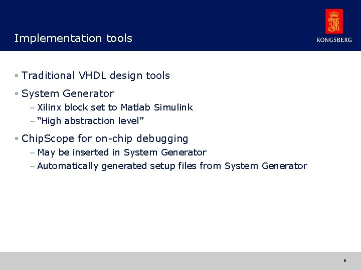
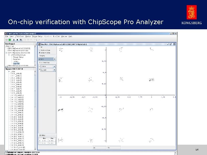
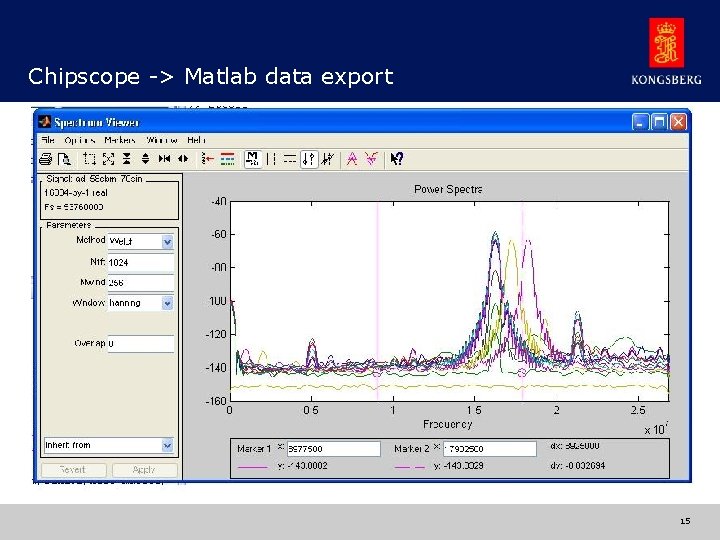
Implementation tools § Traditional VHDL design tools § System Generator – Xilinx block set to Matlab Simulink – “High abstraction level” § Chip. Scope for on-chip debugging – May be inserted in System Generator – Automatically generated setup files from System Generator © KONGSBERG 26 August 2003 8

© KONGSBERG 26 August 2003 9

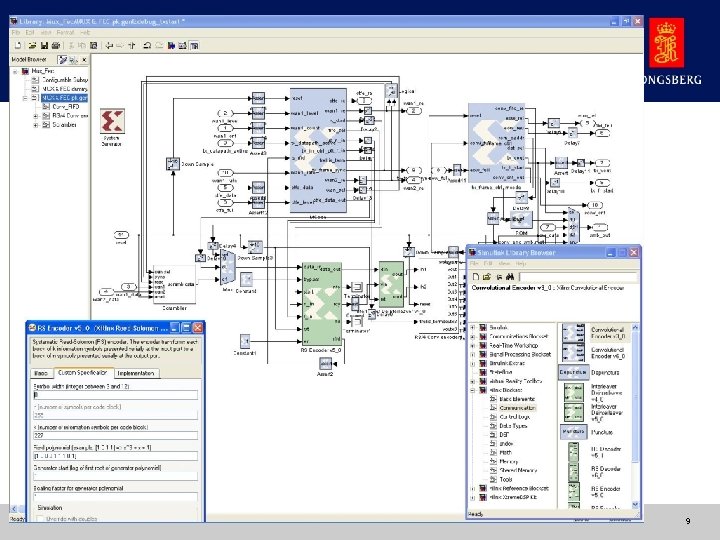
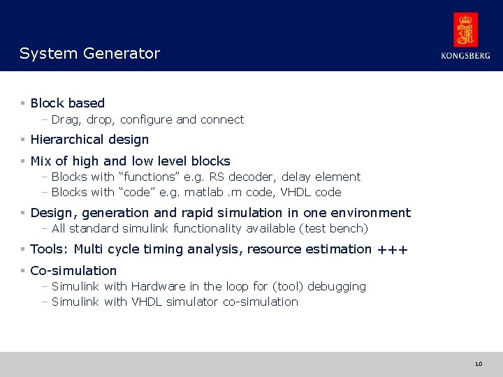
System Generator § Block based – Drag, drop, configure and connect § Hierarchical design § Mix of high and low level blocks – Blocks with “functions” e. g. RS decoder, delay element – Blocks with “code” e. g. matlab. m code, VHDL code § Design, generation and rapid simulation in one environment – All standard simulink functionality available (test bench) § Tools: Multi cycle timing analysis, resource estimation +++ § Co-simulation – Simulink with Hardware in the loop for (tool) debugging – Simulink with VHDL simulator co-simulation © KONGSBERG 26 August 2003 10

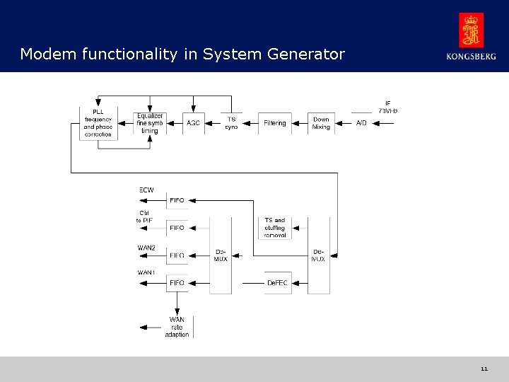
Modem functionality in System Generator © KONGSBERG 26 August 2003 11

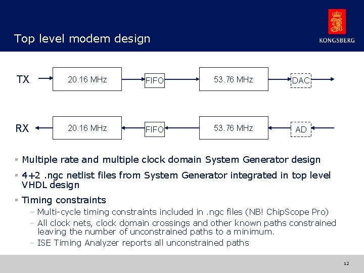
Top level modem design TX 20. 16 MHz FIFO 53. 76 MHz DAC RX 20. 16 MHz FIFO 53. 76 MHz AD § Multiple rate and multiple clock domain System Generator design § 4+2. ngc netlist files from System Generator integrated in top level VHDL design § Timing constraints – Multi-cycle timing constraints included in. ngc files (NB! Chip. Scope Pro) – All clock nets, clock domain crossings and other known paths constrained leaving the number of unconstrained paths to a minimum. – ISE Timing Analyzer reports all unconstrained paths © KONGSBERG 26 August 2003 12

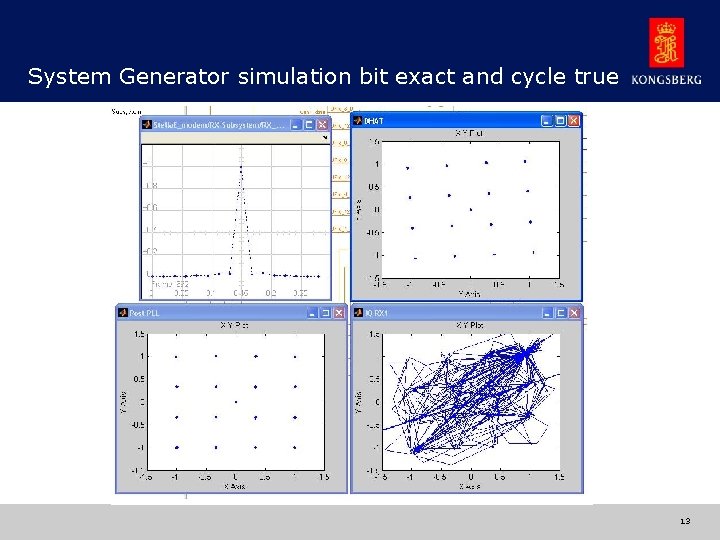
System Generator simulation bit exact and cycle true © KONGSBERG 26 August 2003 13

On-chip verification with Chip. Scope Pro Analyzer © KONGSBERG 26 August 2003 14

Chipscope -> Matlab data export © KONGSBERG 26 August 2003 15

Experiences § “System level” implementation with System Generator – High level / conceptual input specifications – High level rapid implementation by system/DSP engineers – Joint system design and implementation – System Generator also used by FPGA designers in modem design – Relatively high speed simulations -Simulink simulations used to verify data path implementation -VHDL simulation used to verify top level functionality -System Generator VHDL output used to verify datapath interfaces to top level design -NOT Used for performance simulations !!!! (m code modelsused) – Integrates well with top level VHDL design © KONGSBERG 26 August 2003 16

Experiences § Thank heaven for on-chip logic analyzers such as Chip. Scope – Highly integrated with System Generator § Tool quality acceptable – A few bugs related to simulation – A few bugs related to code generation – Debugged by using HW in the loop (highly integrated in System Generator) § => Time saved (development cost and time to market) © KONGSBERG 26 August 2003 17