High Efficiency Klystron Design and Simulations Chiara Marrelli

- Slides: 35

High Efficiency Klystron Design and Simulations Chiara Marrelli, Wednesday

Introduction Design of high efficiency power klystron to meet the large power needs of CLIC: Goal efficiency above 70% (state of the art is around 65%) The design is based on some basic ideas: 1. Go to extremely low perveance; 2. Use of high harmonic cavities (2 nd and 3 rd) 3. Optimization of the output cavity; 4. Single beam device (low power – possible use of more devices in parallel).

Outline Part 1: � Simulations and optimization with AJDisk, a dedicated 1 -D klystron code from SLAC; � Idler cavities RF design (SUPERFISH, HFSS); � Input cavity (and coupler) RF design (HFSS); � Gdfid. L PIC simulations. Part 2: � Traveling Wave Output cavity design and issues.

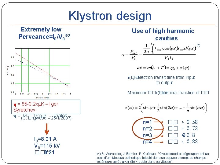
Klystron design Extremely low Perveance=I 0/V 03/2 Use of high harmonic cavities (*) τ(�� )=electron transit time from input to output Maximum ��τ(�� for ) periodic function of �� η = 85 -0. 2 x K – Igor Syratchev η = (C. 78 -0. 16 x K - Thales Lingwood – 25/1/2007) I 0=8. 21 A V 0=115 k. V ��P= 0. 21 n=2 n=3 n=4 �� �� ≈ 0. 58 ≈ 0. 73 ≈0 0. 8 ≈ 0. 83 (*) R. Warnecke, J. Bernier, P. Guénard, “Groupement et dégroupement au sein d’un faisceau cathodique injecté dens un espace exempt de champs extérieurs après avoir été modulé dans sa vitesse”.

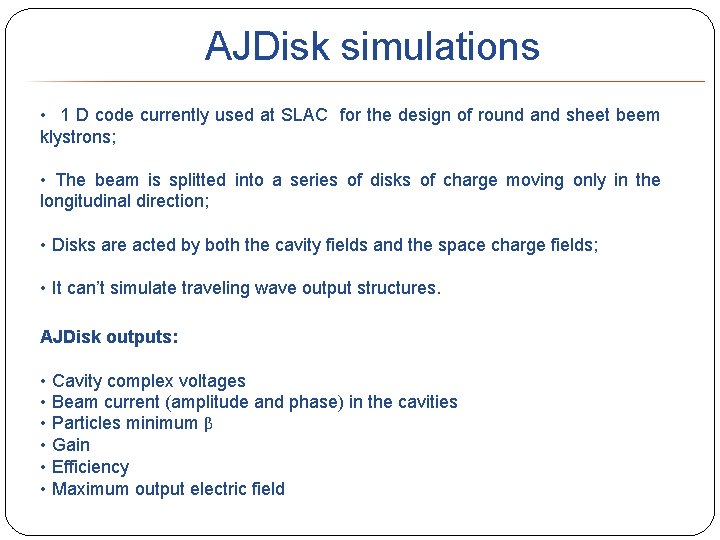
AJDisk simulations • 1 D code currently used at SLAC for the design of round and sheet beem klystrons; • The beam is splitted into a series of disks of charge moving only in the longitudinal direction; • Disks are acted by both the cavity fields and the space charge fields; • It can’t simulate traveling wave output structures. AJDisk outputs: • Cavity complex voltages • Beam current (amplitude and phase) in the cavities • Particles minimum β • Gain • Efficiency • Maximum output electric field

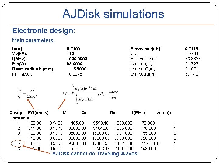
AJDisk simulations Electronic design: Main parameters: Io(A): Vo(k. V): f(MHz): Pin(W): Beam radius b (mm): Fill Factor: Cavity RQ(ohms) M Harmonic 1 180. 00 0. 9400 2 211. 00 0. 9378 3 120. 00 0. 9310 4 118. 00 0. 8850 5 84. 60 0. 9358 6 185. 00 0. 9400 8. 2100 115 1000. 0000 93. 0000 5. 5000 0. 6875 Qe 485. 00 95000. 00 50. 00 Perveance(u. K): v/c: Beta. E(rad/m): Lambda(m): Lambda. P(m): Lambda. Q(m): Qo 9593. 48 9464. 26 15300. 00 12300. 00 17407. 90 9593. 48 f(MHz) 1000. 000 1005. 000 1981. 000 2983. 000 1011. 000 1000. 000 AJDisk cannot do Traveling Waves! 0. 2118 0. 5764 36. 3363 0. 1729 0. 4671 5. 1443 z(mm)) 70. 000 170. 000 455. 000 720. 000 1290. 000 1580. 000 1 1 2 3 1 1

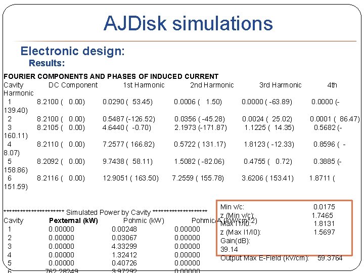
AJDisk simulations Electronic design: Results: FOURIER COMPONENTS AND PHASES OF INDUCED CURRENT Cavity DC Component 1 st Harmonic 2 nd Harmonic 1 8. 2100 ( 0. 00) 0. 0290 ( 53. 45) 0. 0006 ( 1. 50) 139. 40) 2 8. 2100 ( 0. 00) 0. 5487 (-126. 52) 0. 0356 ( -45. 28) 3 8. 2105 ( 0. 00) 4. 6440 ( -0. 70) 2. 1973 (-171. 87) 160. 11) 4 8. 2110 ( 0. 00) 7. 2577 ( 166. 82) 0. 5722 ( 131. 17) 8. 07) 5 8. 2092 ( 0. 00) 9. 7438 ( 58. 11) 1. 5082 ( -82. 06) 158. 86) 6 8. 2116 ( 0. 00) 12. 9051 ( 163. 50) 7. 2559 ( 155. 78) 151. 59) 3 rd Harmonic 4 th 0. 0000 ( -63. 89) 0. 0000 (- 0. 0024 ( 25. 02) 1. 1225 ( 14. 35) 0. 0001 ( 86. 47) 0. 5682 (- 1. 8123 ( -12. 33) 0. 8596 ( - 0. 4755 ( 0. 72) 0. 3885 (- 3. 6206 ( 153. 41) 1. 8711 ( Min v/c: 0. 0175 *********** Simulated Power by Cavity ********** z (Min v/c): 1. 7465 Cavity Pexternal (k. W) Pohmic/AMax (k. W/cm^2) I 1/I 0: 1. 8131 1 0. 00000 0. 00248 0. 00000 z (Max I 1/I 0): 1. 5697 2 0. 00000 0. 03067 0. 00000 Gain(d. B): 3 0. 00000 4. 33299 0. 00000 39. 14 4 0. 00000 1. 32412 0. 00000 Output Max E-Field (k. V/cm): 59. 3764 5 0. 00000 0. 40726 0. 00000

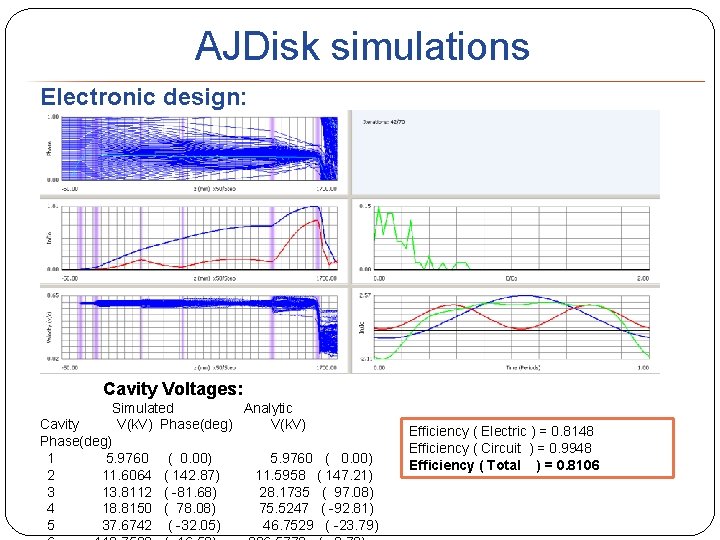
AJDisk simulations Electronic design: Cavity Voltages: Simulated Analytic Cavity V(k. V) Phase(deg) 1 5. 9760 ( 0. 00) 2 11. 6064 ( 142. 87) 11. 5958 ( 147. 21) 3 13. 8112 ( -81. 68) 28. 1735 ( 97. 08) 4 18. 8150 ( 78. 08) 75. 5247 ( -92. 81) 5 37. 6742 ( -32. 05) 46. 7529 ( -23. 79) Efficiency ( Electric ) = 0. 8148 Efficiency ( Circuit ) = 0. 9948 Efficiency ( Total ) = 0. 8106

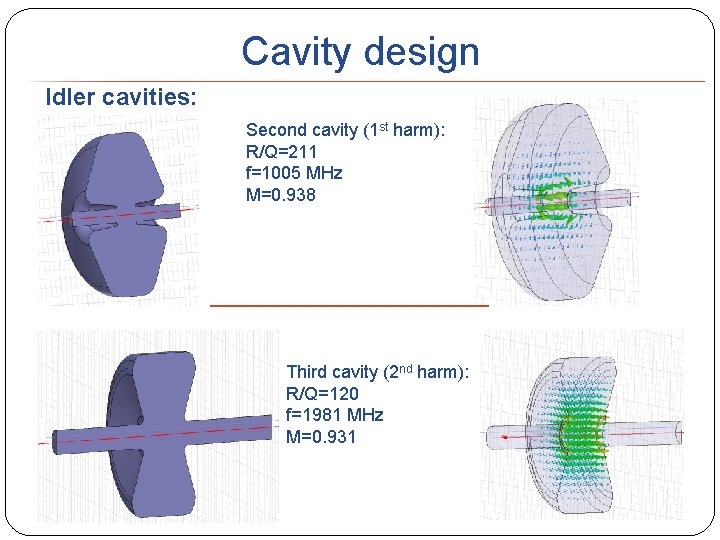
Cavity design Idler cavities: Second cavity (1 st harm): R/Q=211 f=1005 MHz M=0. 938 Third cavity (2 nd harm): R/Q=120 f=1981 MHz M=0. 931

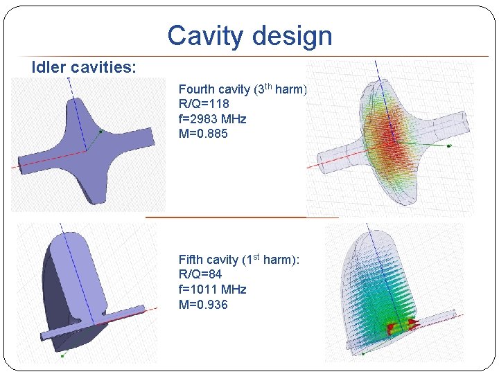
Cavity design Idler cavities: Fourth cavity (3 th harm): R/Q=118 f=2983 MHz M=0. 885 Fifth cavity (1 st harm): R/Q=84 f=1011 MHz M=0. 936

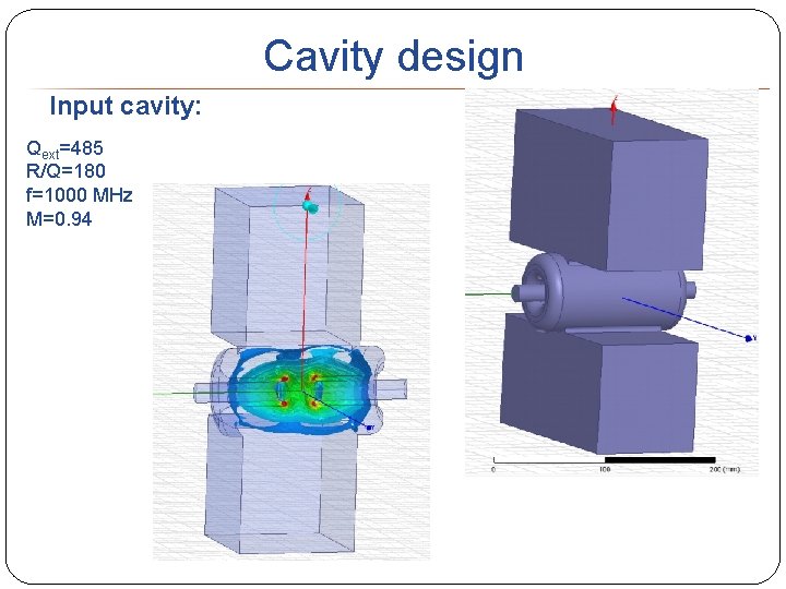
Cavity design Input cavity: Qext=485 R/Q=180 f=1000 MHz M=0. 94

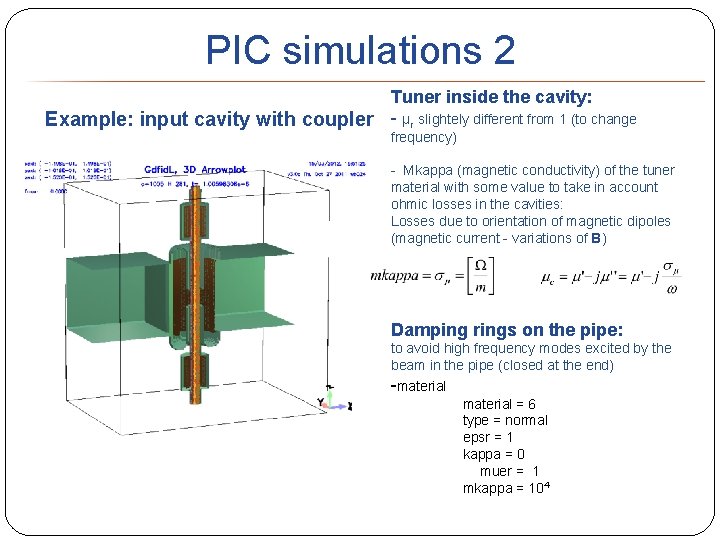
PIC simulations 1 First round of simulations with Gdfid. L: simulation of first three cavities (before optimization): • running on one single machine (8 cores) • large mesh (2 mm – beam radius is 5. 5 mm) • simulation time ~ 1 week (for t=10 μs) For the PIC simulation with Gdfid. L we have to take in account that: 1. Gdfid. L cannot simulate losses in copper; we need to introduce some loss mechanism in cavities (easy) and pipes (to avoid high frequency modes excited by the beam); 2. Since we are using a very large mesh (to reduce simulation time), if we keep the same geometry as in HFSS for cavities we are off in frequency: this is why we have to introduce tuners, and if it is not enough, we also have to change a bit the geometry; 3. To calculate the external Q for the input cavity we need to simulate the input cavity also in time domain.

PIC simulations 2 Tuner inside the cavity: Example: input cavity with coupler - μr slightely different from 1 (to change frequency) - Mkappa (magnetic conductivity) of the tuner material with some value to take in account ohmic losses in the cavities: Losses due to orientation of magnetic dipoles (magnetic current - variations of B) Damping rings on the pipe: to avoid high frequency modes excited by the beam in the pipe (closed at the end) -material = 6 type = normal epsr = 1 kappa = 0 muer = 1 mkappa = 104

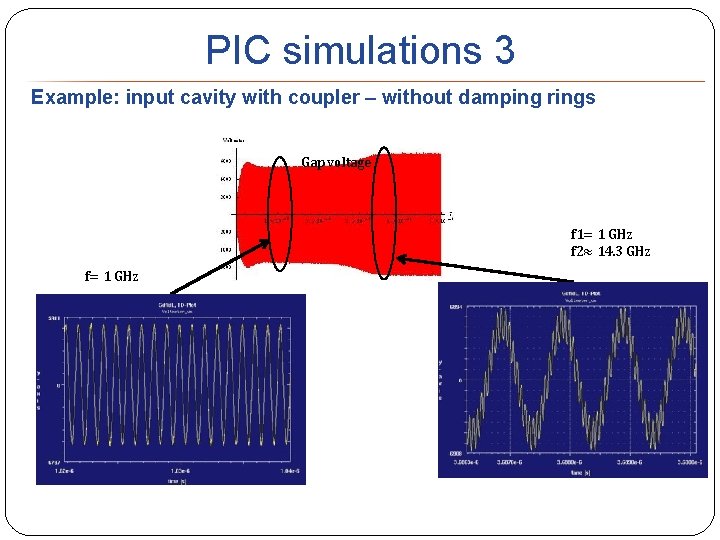
PIC simulations 3 Example: input cavity with coupler – without damping rings Gap voltage f 1= 1 GHz f 2≈ 14. 3 GHz f= 1 GHz

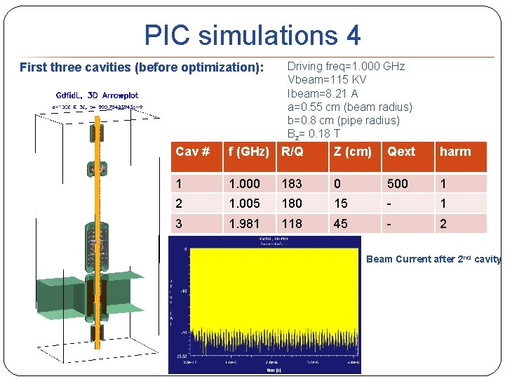
PIC simulations 4 First three cavities (before optimization): Driving freq=1. 000 GHz Vbeam=115 KV Ibeam=8. 21 A a=0. 55 cm (beam radius) b=0. 8 cm (pipe radius) Bz= 0. 18 T Cav # f (GHz) R/Q Z (cm) Qext harm 1 1. 000 183 0 500 1 2 1. 005 180 15 - 1 3 1. 981 118 45 - 2 Beam Current after 2 nd cavity

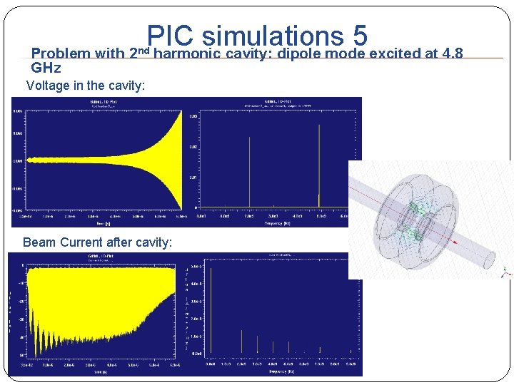
Problem with GHz PIC simulations 5 harmonic cavity: dipole mode excited at 4. 8 2 nd Voltage in the cavity: Beam Current after cavity:

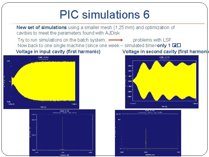
PIC simulations 6 New set of simulations using a smaller mesh (1. 25 mm) and optimization of cavities to meet the parameters found with AJDisk Try to run simulations on the batch system. . . problems with LSF Now back to one single machine (since one week – simulated time=only 1 �� s): Voltage in input cavity (first harmonic) Voltage in second cavity (first harmonic

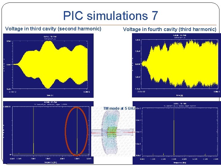
PIC simulations 7 Voltage in third cavity (second harmonic) Voltage in fourth cavity (third harmonic) TM mode at 5 GHz

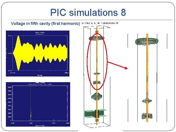
PIC simulations 8 Voltage in fifth cavity (first harmonic)

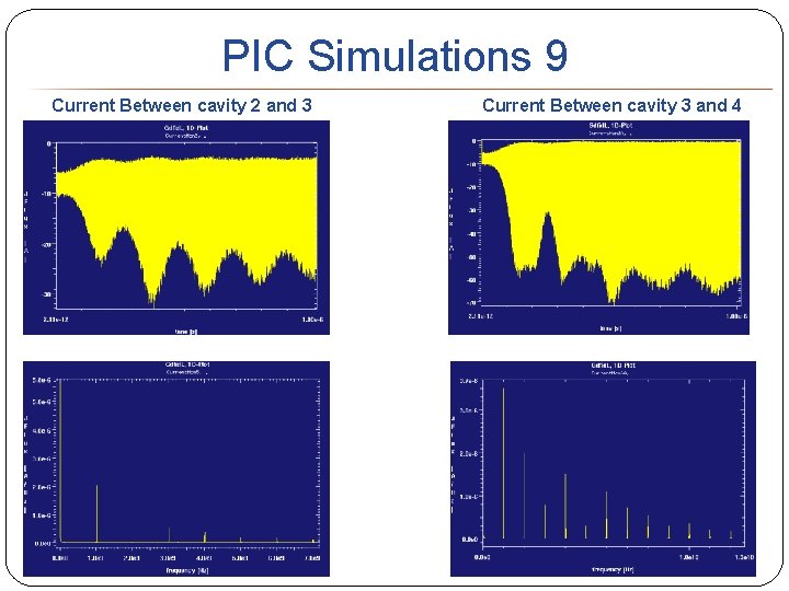
PIC Simulations 9 Current Between cavity 2 and 3 Current Between cavity 3 and 4

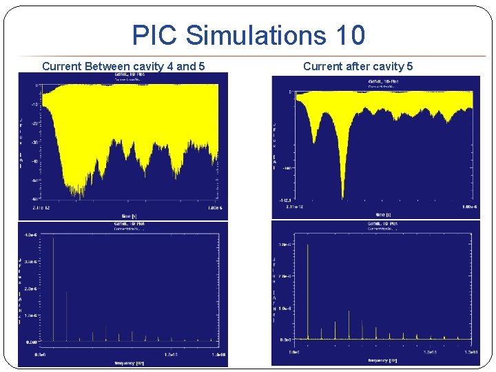
PIC Simulations 10 Current Between cavity 4 and 5 Current after cavity 5

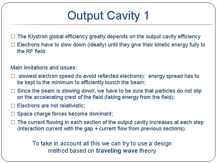
Output Cavity 1 � The Klystron global efficiency greatly depends on the output cavity efficiency � Electrons have to slow down (ideally) until they give their kinetic energy fully to the RF field Main limitations and issues: � slowest electron speed (to avoid reflected electrons): energy spread has to be kept to the minimum to efficiently bunch the beam; � Since the beam is slowing down, we have to be sure that particles do not slip on the accelerating crest of the field (taking energy from the field); � Electrons are not relativistic; � Space charge forces become dominant; � The current flowing in each section of the output cavity increases at each step (interaction current with the gap + current flow from previous sections). To take in account all this we can try to use a design method based on traveling wave theory

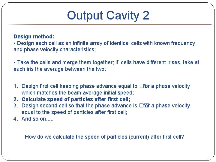
Output Cavity 2 Design method: • Design each cell as an infinite array of identical cells with known frequency and phase velocity characteristics; • Take the cells and merge them together; if cells have different irises, take at each iris the average between the two; 1. Design first cell keeping phase advance equal to �� for a phase velocity which matches the beam average initial speed; 2. Calculate speed of particles after first cell; 3. Design second cell so that the phase advance is �� for a phase velocity equal to the speed of particles after first cell; 4. And so on. . . How do we calculate the speed of particles (current) after first cell?

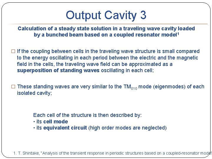
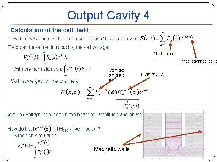
Output Cavity 3 Calculation of a steady state solution in a traveling wave cavity loaded by a bunched beam based on a coupled resonator model 1 � If the coupling between cells in the traveling wave structure is small compared to the energy oscillating in each period between the electric and the magnetic field in the cells, the traveling wave field can be approximated as a superposition of standing waves oscillating in each cell; � These standing waves are very similar to the TM 010 mode (eigenmodes) of each isolated cavity; Each cell of the structure is then described by: • its cell mode • its equivalent circuit (high order modes are neglected) 1. T. Shintake, “Analysis of the transient response in periodic structures based on a coupled-resonator model”

Output Cavity 4 Calculation of the cell field: Traveling wave field is then represented as (1 D approximation): Field can be written introducing the cell voltage: Mode of cell n With the normalization: Complex amplitud e So that we get, for the total field: Field profile Complex voltage depends on the beam for amplitude and phase. How do I get (TM 010 - like mode) ? Superfish simulation: Magnetic walls Phase advance per c

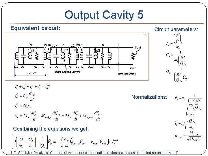
Output Cavity 5 Equivalent circuit: Circuit parameters: 1 Normalizations: Combining the equations we get: 1. T. Shintake, “Analysis of the transient response in periodic structures based on a coupled-resonator model”

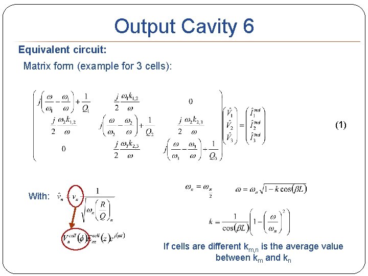
Output Cavity 6 Equivalent circuit: Matrix form (example for 3 cells): (1) With: If cells are different km, n is the average value between km and kn

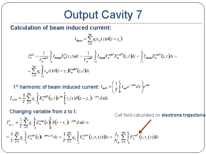
Output Cavity 7 Calculation of beam induced current: 1 st harmonic of beam induced current: Changing variable from z to t: Cell field calculated on electrons trajectories

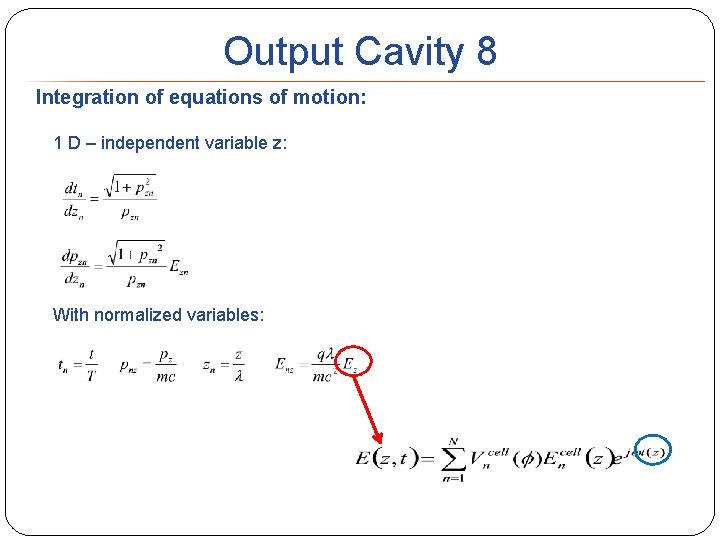
Output Cavity 8 Integration of equations of motion: 1 D – independent variable z: With normalized variables:

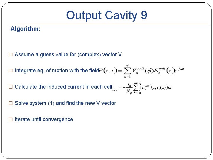
Output Cavity 9 Algorithm: � Assume a guess value for (complex) vector V � Integrate eq. of motion with the field � Calculate the induced current in each cell � Solve system (1) and find the new V vector � Iterate until convergence

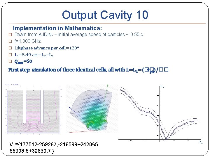
Output Cavity 10 Implementation in Mathematica: � Beam from AJDisk – initial average speed of particles ~ 0. 55 c � f=1. 000 GHz � �� =phase advance per cell=120° � L 1=5. 49 cm=L 2=L 3 � Qext 3=50 First step: simulation of three identical cells, all with L=L 1=(�� vph)/�� pn V 1={177512 -259263, -216599+242065 , 55308. 5+32690. 7 } zn

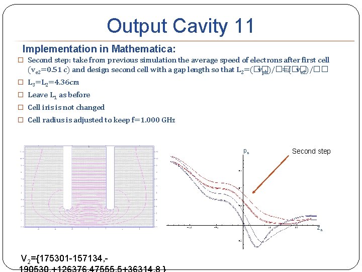
Output Cavity 11 Implementation in Mathematica: � Second step: take from previous simulation the average speed of electrons after first cell (ve 2=0. 51 c) and design second cell with a gap length so that L 2=(�� vph)/�� =(�� ve 2)/�� � L 3=L 2=4. 36 cm � Leave L 1 as before � Cell iris is not changed � Cell radius is adjusted to keep f=1. 000 GHz pn Second step zn V 2={175301 -157134, -

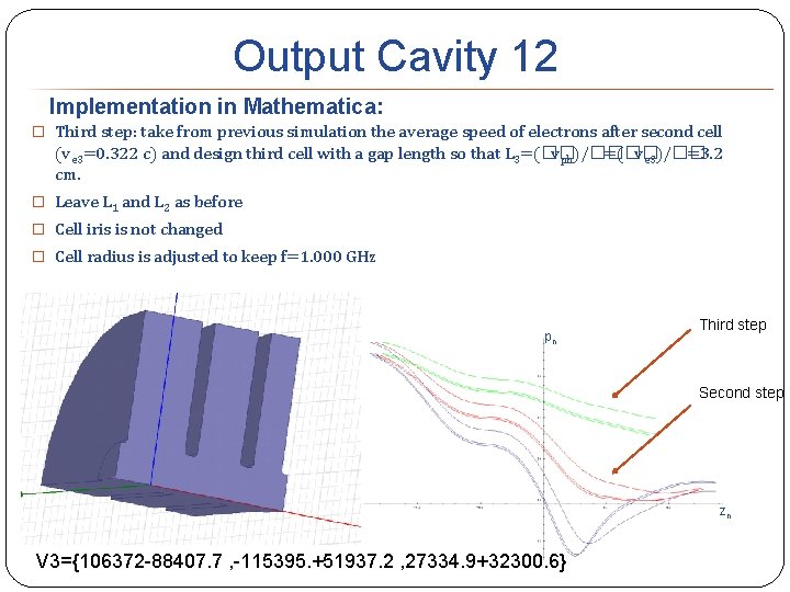
Output Cavity 12 Implementation in Mathematica: � Third step: take from previous simulation the average speed of electrons after second cell (ve 3=0. 322 c) and design third cell with a gap length so that L 3=(�� vph)/�� =(�� ve 3)/�� =3. 2 cm. � Leave L 1 and L 2 as before � Cell iris is not changed � Cell radius is adjusted to keep f=1. 000 GHz pn Third step Second step zn V 3={106372 -88407. 7 , -115395. +51937. 2 , 27334. 9+32300. 6}

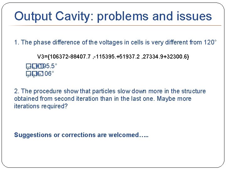
Output Cavity: problems and issues 1. The phase difference of the voltages in cells is very different from 120° V 3={106372 -88407. 7 , -115395. +51937. 2 , 27334. 9+32300. 6} �� 2 -�� 1=195. 5° �� 3 -�� 2=-106° 2. The procedure show that particles slow down more in the structure obtained from second iteration than in the last one. Maybe more iterations required? Suggestions or corrections are welcomed…. .

Thank you for your attention! And thanx to A. D’Elia and R. Wegner for their help!