EMT 352 ADVANCED DEVICES Assignment I Examination Question

 Atalla and Dawon Kahng at")
 Symbols and basic construction for both configurations of MOSFETs")
 Sketch the basic structure of CMOS and label all element")
 Give two application of MOSFETs and two basic properties of MOSFETs Applications v.")
 By referring to the NMOS structure view shown in Figure 1. 0. Discuss")
 Cutoff Region (Vgs = 0 V) v. When the gate is at a")
 Linear Region (Vgs > Vth and Vds < Vgs – Vth) v When")
 Saturation Region (Vgs > Vth and Vds ≥ Vgs – Vth) v. Vds")
 An n. MOS transistor has a width to length ratio (W/L) that is")


- Slides: 15
EMT 352 ADVANCED DEVICES Assignment I -Examination Question and the Answer. NAME MATRIC NO MOHD SHAHRUL NIZAM BIN MOHD SIDEK 151010510 MUHAMMAD AZAMUDDIN BIN ADNAN 151010512 NUR AZIZAN BIN ANUAR 151010529 MUHAMMAD FIRDAUS BIN AZMAN 151013292 MOHAMMAD HASHAMUDDIN BIN JACHO 151010508 MUHAMAD FAISAL BIN SAMSUDIN 151010511 MOHAMMAD SHAFIQ YADI BIN MOHAMMAD 151010512 MALACK
Answer All The Question In 1959 M. M. (John) Atalla and Dawon Kahng at Bell Labs achieved the first successful insulated-gate field-effect transistor (FET), which had been long anticipated by Lilienfeld, Heil, Shockley and others (1926 Milestone) by overcoming the "surface states" that blocked electric fields from penetrating into the semiconductor material.
i) Symbols and basic construction for both configurations of MOSFETs
ii) Sketch the basic structure of CMOS and label all element
iii) Give two application of MOSFETs and two basic properties of MOSFETs Applications v. Microprocessors v. Memories v. Power Devices Basic Properties v. Unipolar device v. Very high input impedance v. Capable of power gain v 3/4 terminal device, G, S, D, B v. Two possible device types: enhancement mode; depletion mode v. Two possible channel types: n-channel; p-channel
(B) By referring to the NMOS structure view shown in Figure 1. 0. Discuss the n-mos operation at the condition. I) Cutoff Region (3 Marks) II) Linear Region (3 Marks) III) Saturation Region (3 Marks) Figure 1. 0: NMOS Structure View
i) Cutoff Region (Vgs = 0 V) v. When the gate is at a low voltage v. P-type body is at low voltage v. Source-body and drain-body diodes are in reverse bias thus, not allowing vcurrent to flow between Drain and Source. No current flows, transistor is OFF
II) Linear Region (Vgs > Vth and Vds < Vgs – Vth) v When the gate is at a high voltage v Positive charge on gate of MOS capacitor v Negative charge attracted to body v Inverts a channel under gate to n-type v Now current can flow through n-type silicon from source through channel to drain, transistor is ON
III) Saturation Region (Vgs > Vth and Vds ≥ Vgs – Vth) v. Vds increases, the voltage at the drain side of the channel is increases v. Depletion region at the drain will increases as compared to the source (the bulk-drain diode is more reverse biased) v. At one point the depletion region become so big until it push the channel to the surface increasing Vds will result in a tapered (narrowing) channel v. The Ids-Vds curve does not continue as a straight line.
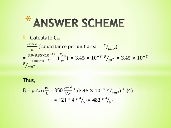
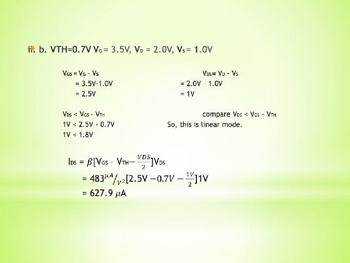
(C) An n. MOS transistor has a width to length ratio (W/L) that is equal to 4. The gate oxide thickness for the device is 100 Å, the mobility of electron is 350 cm 2/Vs. Determine the operation mode and calculated the IDS based on VGS value for the given following voltage. (Assume VTH = 0. 7 V) i. Calculate C and β = µ C ii. Determine the operation region and calculate the ox n ox Ids based on Vgs values at: a. V b. V c. V G = 1. 5 V, VD = 2. 0 V, VS = 0. 3 V G = 3. 5 V, VD = 2. 0 V, VS = 1. 0 V G = 0. 8 V, VD = 1. 0 V, VS = 0. 5 V
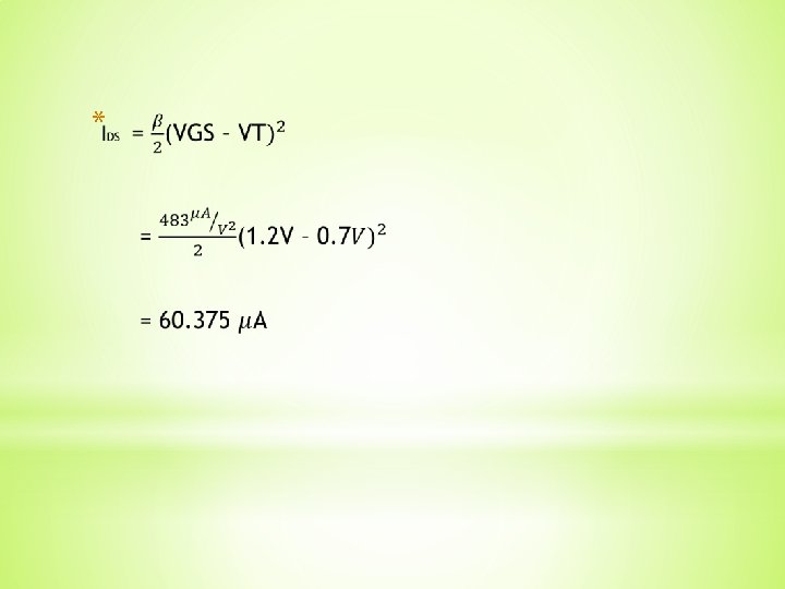
ii. a. VTH = 0. 7 V VG = 1. 5 V, VD = 2. 0 V, VS = 0. 3 V VGS = VG - VS = 1. 5 V- 0. 3 V = 1. 2 V VDS ≥ VGS-VTH VDS= VD - VS = 2. 0 V – 0. 3 V = 1. 7 V compare VDS ≥ VGS – VTH 1. 7 V ≥ 1. 2 V-0. 7 V So, this is saturation mode. 1. 7 V ≥ 0. 5 V
iii. c. VTH = 0. 7 V V G = 0. 8 V, VD = 1. 0 V, VS = 0. 5 V VGS = VG - VS = 0. 8 V - 0. 5 V = 0. 3 V VGS ≤ VTH 0. 3 V ≤ 0. 7 V IDS = 0 VDS= VD - VS = 1. 0 V – 0. 5 V = 0. 5 V compare VDS ≤ VGS So, this is cutoff mode.