EE 580 Solar Cells Todd J Kaiser Lecture
- Slides: 49

EE 580 – Solar Cells Todd J. Kaiser • Lecture 06 • Solar Cell Materials & Structures Montana State University: Solar Cells Lecture 6: Solar Cells 1

Solar Cell Technologies • A) Crystalline Silicon • B) Thin Film • C) Group III-IV Cells Montana State University: Solar Cells Lecture 6: Solar Cells 2

A) Crystalline Silicon • Most common for commercial applications • Advantages – Well known standard processing – Silicon is very abundant • Disadvantages – Requires expensive highly pure silicon – Competes for silicon with electronics industry Montana State University: Solar Cells Lecture 6: Solar Cells 3

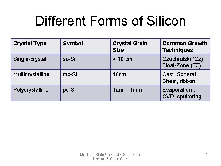
Types of Crystalline Silicon • Carefully made Silicon forms crystals. Different levels of crystal structure may exist ranging from single crystal to totally non-crystalline – Single crystal silicon – Multi-crystal silicon – Polycrystalline – Ribbon silicon – Amorphous silicon • The main difference between each is the crystal grain size and their growth technique Montana State University: Solar Cells Lecture 6: Solar Cells 4

Different Forms of Silicon Crystal Type Symbol Crystal Grain Size Common Growth Techniques Single-crystal sc-Si > 10 cm Czochralski (Cz), Float-Zone (FZ) Multicrystalline mc-Si 10 cm Cast, Spheral, Sheet, ribbon Polycrystalline pc-Si 1 mm – 1 mm Evaporation , CVD, sputtering Montana State University: Solar Cells Lecture 6: Solar Cells 5

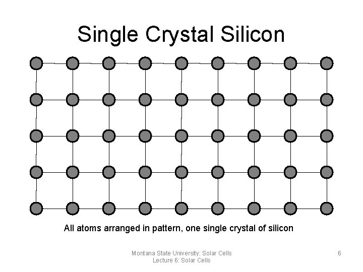
Single Crystal Silicon All atoms arranged in pattern, one single crystal of silicon Montana State University: Solar Cells Lecture 6: Solar Cells 6

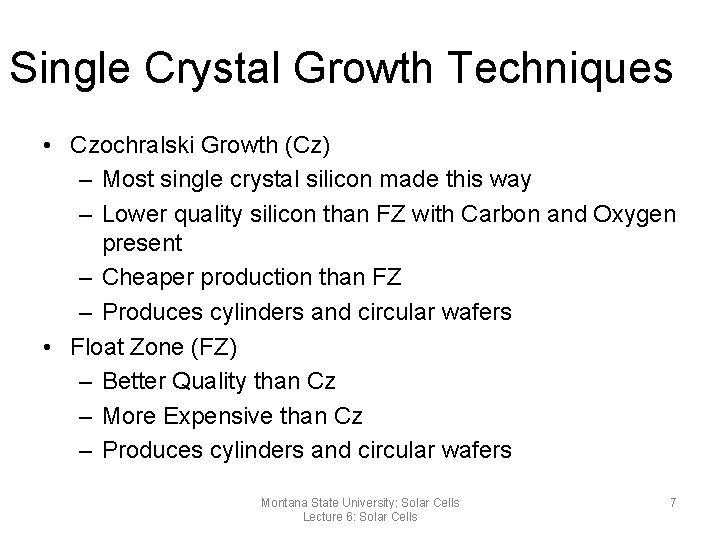
Single Crystal Growth Techniques • Czochralski Growth (Cz) – Most single crystal silicon made this way – Lower quality silicon than FZ with Carbon and Oxygen present – Cheaper production than FZ – Produces cylinders and circular wafers • Float Zone (FZ) – Better Quality than Cz – More Expensive than Cz – Produces cylinders and circular wafers Montana State University: Solar Cells Lecture 6: Solar Cells 7

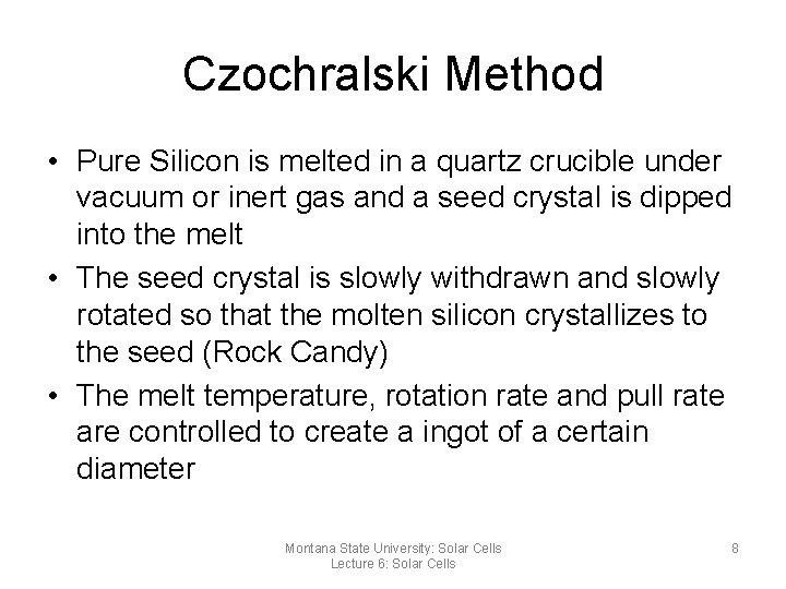
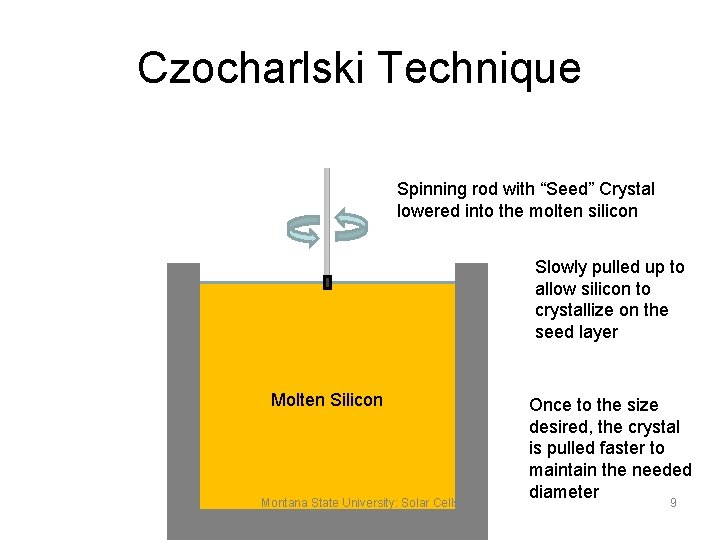
Czochralski Method • Pure Silicon is melted in a quartz crucible under vacuum or inert gas and a seed crystal is dipped into the melt • The seed crystal is slowly withdrawn and slowly rotated so that the molten silicon crystallizes to the seed (Rock Candy) • The melt temperature, rotation rate and pull rate are controlled to create a ingot of a certain diameter Montana State University: Solar Cells Lecture 6: Solar Cells 8

Czocharlski Technique Spinning rod with “Seed” Crystal lowered into the molten silicon Slowly pulled up to allow silicon to crystallize on the seed layer Molten Silicon Montana State University: Solar Cells Lecture 6: Solar Cells Once to the size desired, the crystal is pulled faster to maintain the needed diameter 9

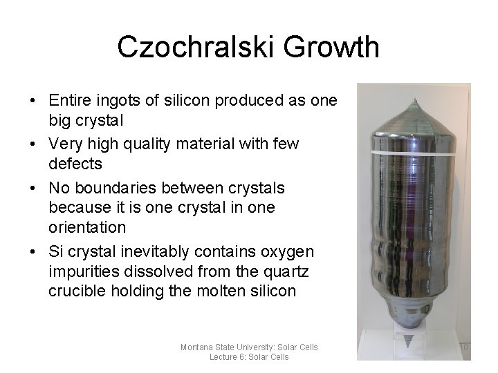
Czochralski Growth • Entire ingots of silicon produced as one big crystal • Very high quality material with few defects • No boundaries between crystals because it is one crystal in one orientation • Si crystal inevitably contains oxygen impurities dissolved from the quartz crucible holding the molten silicon Montana State University: Solar Cells Lecture 6: Solar Cells 10

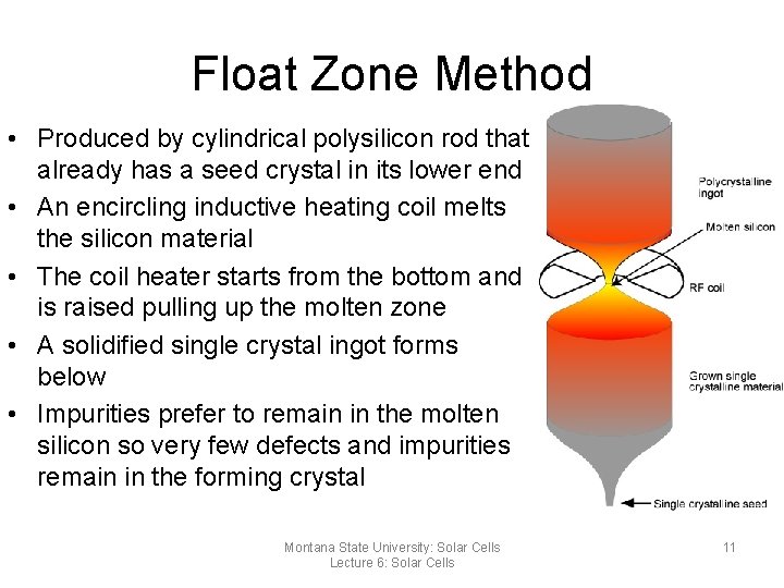
Float Zone Method • Produced by cylindrical polysilicon rod that already has a seed crystal in its lower end • An encircling inductive heating coil melts the silicon material • The coil heater starts from the bottom and is raised pulling up the molten zone • A solidified single crystal ingot forms below • Impurities prefer to remain in the molten silicon so very few defects and impurities remain in the forming crystal Montana State University: Solar Cells Lecture 6: Solar Cells 11

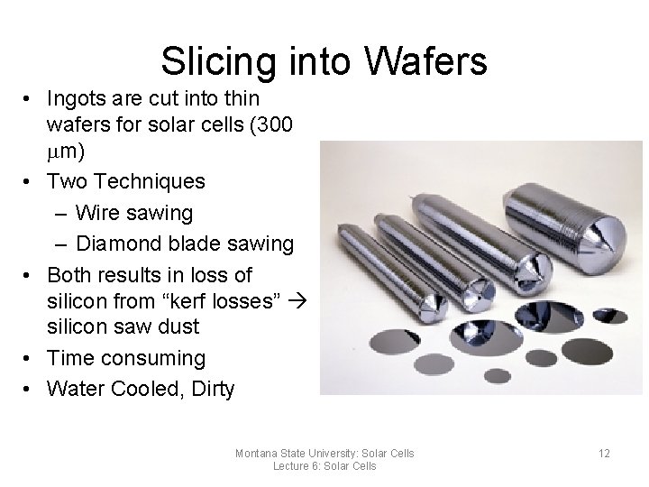
Slicing into Wafers • Ingots are cut into thin wafers for solar cells (300 mm) • Two Techniques – Wire sawing – Diamond blade sawing • Both results in loss of silicon from “kerf losses” silicon saw dust • Time consuming • Water Cooled, Dirty Montana State University: Solar Cells Lecture 6: Solar Cells 12

Single Crystal Silicon • What we are using • Currently supplies a significant but declining solar cell market share • Advantages – Produced for electronics industry – Allows for higher efficiency solar cells • Disadvantages – Requires higher quality of feed stock – More expensive and slower to produce – Circular shape leads to lower packing density in panels or larger waste of silicon Montana State University: Solar Cells Lecture 6: Solar Cells 13

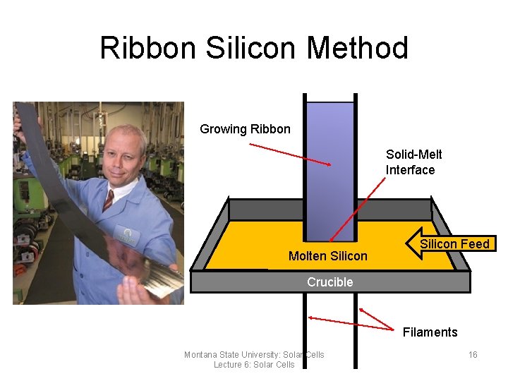
Ribbon Silicon • Ribbon silicon is a technique used to grow multicrystalline silicon • Two graphite filaments are placed in a crucible of molten silicon • The molten silicon is grown horizontally through capillary action along the filaments • Produces a ribbon-like sheet of multi-crystalline silicon which is already a long wafer no kerf losses Montana State University: Solar Cells Lecture 6: Solar Cells 14

Ribbon Silicon (+/-) • Advantages – Thickness can be varied by the filament width & the pull speed – Cheaper - less wasted silicon due to sawing wafers • Disadvantages – Lower Solar Cell Efficiencies due to more defects – Irregular surface characteristics leading to poorer cell performance Montana State University: Solar Cells Lecture 6: Solar Cells 15

Ribbon Silicon Method Growing Ribbon Solid-Melt Interface Molten Silicon Feed Crucible Filaments Montana State University: Solar Cells Lecture 6: Solar Cells 16

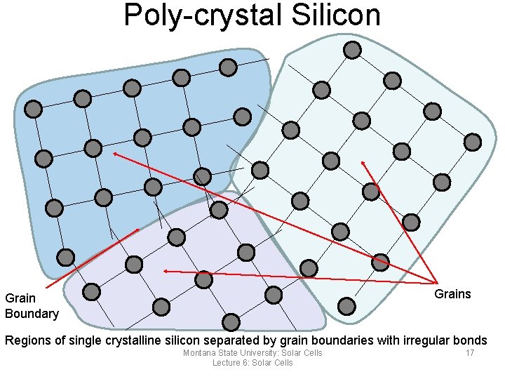
Poly-crystal Silicon Grains Grain Boundary Regions of single crystalline silicon separated by grain boundaries with irregular bonds Montana State University: Solar Cells Lecture 6: Solar Cells 17

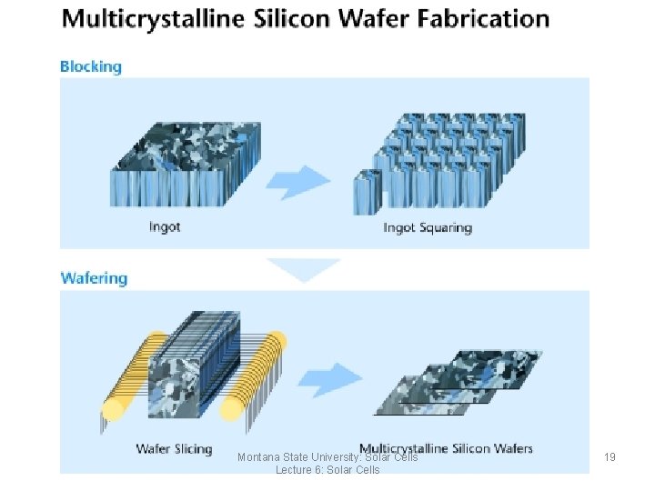
Poly& Multi-Silicon Method • Produced by melting silicon source material in a large rectangular crucible • The material is slowly directionally cooled • Impurities drift to the edges which cool last • These edges are sawn or acid etched off • These blocks are sawn into smaller blocks and then sawn into thin wafers Montana State University: Solar Cells Lecture 6: Solar Cells 18

Multicrystalline Silicon Wafer Fabrication Montana State University: Solar Cells Lecture 6: Solar Cells 19

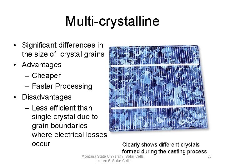
Multi-crystalline • Significant differences in the size of crystal grains • Advantages – Cheaper – Faster Processing • Disadvantages – Less efficient than single crystal due to grain boundaries where electrical losses occur Clearly shows different crystals formed during the casting process Montana State University: Solar Cells Lecture 6: Solar Cells 20

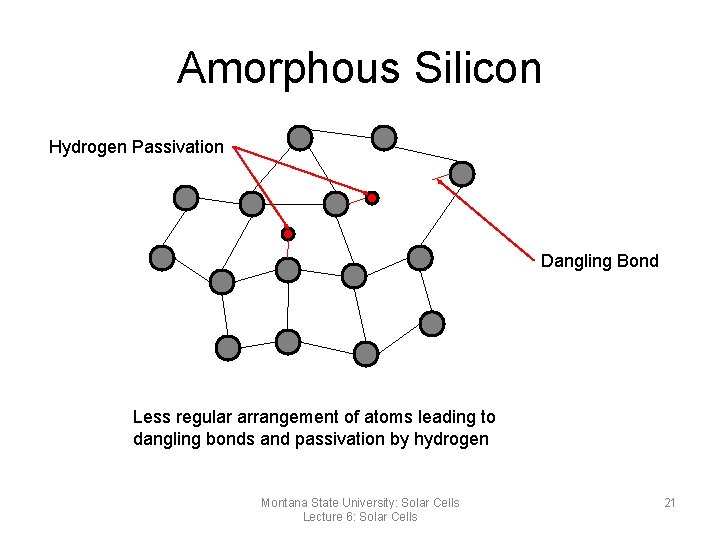
Amorphous Silicon Hydrogen Passivation Dangling Bond Less regular arrangement of atoms leading to dangling bonds and passivation by hydrogen Montana State University: Solar Cells Lecture 6: Solar Cells 21

B) Thin Film • Thin film of semiconductor 1 -10 microns compared to 200 -300 microns • Created by depositing a thin expensive semiconductor on a cheaper glass substrate • Advantages – Requires little semiconductor material – Cheaper to produce: • glass is cheap • semiconductor expensive • Disadvantages – Difficult to manufacture good films – Lower efficiencies Montana State University: Solar Cells Lecture 6: Solar Cells 22

Three Main Thin Films • Amorphous Silicon (a-Si) • Cadmium Telluride (Cd. Te) • Copper Indium Gallium Diselenide (CIGS) Montana State University: Solar Cells Lecture 6: Solar Cells 23

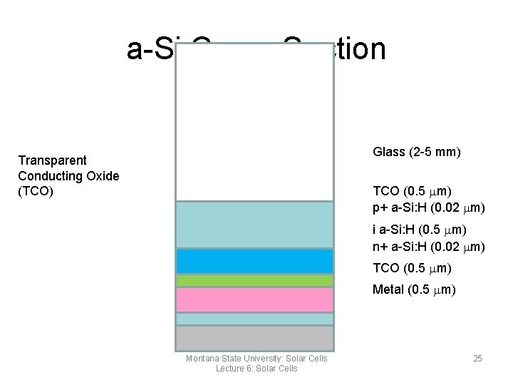
Amorphous Silicon (a-Si) • • Made by evaporating silicon onto a glass base More random orientation than crystalline More electrons not bound to SI atoms Unbounded electrons attract impurities and degrade the electrical performance of the cell • Hydrogen is often added to the material to deactivate the dangling bonds Montana State University: Solar Cells Lecture 6: Solar Cells 24

a-Si Cross-Section Glass (2 -5 mm) Transparent Conducting Oxide (TCO) TCO (0. 5 mm) p+ a-Si: H (0. 02 mm) i a-Si: H (0. 5 mm) n+ a-Si: H (0. 02 mm) TCO (0. 5 mm) Metal (0. 5 mm) Montana State University: Solar Cells Lecture 6: Solar Cells 25

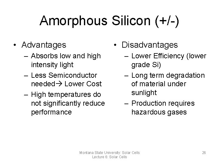
Amorphous Silicon (+/-) • Advantages • Disadvantages – Absorbs low and high intensity light – Less Semiconductor needed Lower Cost – High temperatures do not significantly reduce performance – Lower Efficiency (lower grade Si) – Long term degradation of material under sunlight – Production requires hazardous gases Montana State University: Solar Cells Lecture 6: Solar Cells 26

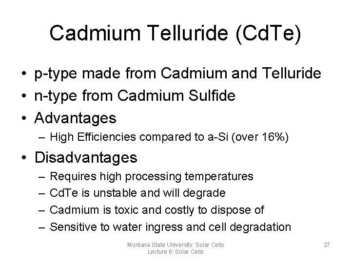
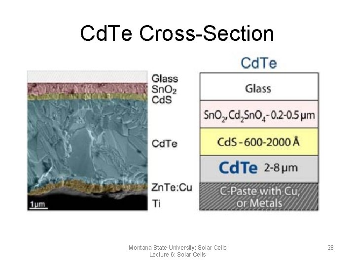
Cadmium Telluride (Cd. Te) • p-type made from Cadmium and Telluride • n-type from Cadmium Sulfide • Advantages – High Efficiencies compared to a-Si (over 16%) • Disadvantages – – Requires high processing temperatures Cd. Te is unstable and will degrade Cadmium is toxic and costly to dispose of Sensitive to water ingress and cell degradation Montana State University: Solar Cells Lecture 6: Solar Cells 27

Cd. Te Cross-Section Montana State University: Solar Cells Lecture 6: Solar Cells 28

Copper Indium Gallium Diselenide (CIGS) • Extremely good light absorption (99% of light absorbed in the first micron) – an optimal and effective PV material • The addition of gallium boosts its light absorption band gap for the solar spectrum • No performance degradation over time • Much higher efficiencies than other thin films (19%) Montana State University: Solar Cells Lecture 6: Solar Cells 29

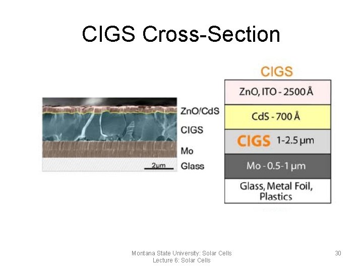
CIGS Cross-Section Montana State University: Solar Cells Lecture 6: Solar Cells 30

CIGS (+/-) • Advantages • Disadvantages – Highest efficiency for thin film cells – Clear pathways to improve performance and efficiencies – Gallium and Indium are scarce materials – Requires expensive vacuum processing Montana State University: Solar Cells Lecture 6: Solar Cells 31

C) Group III-V • Compounds of Group III and V on periodic table • Compound is a material that combines multiple elements in a single structure (not just a mixture) • Used extensively in the electronics and optoelectronics industries as well as space satellites • Makes excellent but very expensive solar cells • Can create multi-junction cells for higher efficiency Montana State University: Solar Cells Lecture 6: Solar Cells 32

Single Junction III-V Cells • Made from combination of two materials – Gallium Arsenide (Ga. As) – Indium Phosphide (In. P) • Best efficiency is at 27. 6% – 1000 W/m 2 of sunlight produces 276 Watts of usable power Montana State University: Solar Cells Lecture 6: Solar Cells 33

Single Junction III-V Cells (+/-) • Advantages • Disadvantages – Very high efficiencies – Low weight – Resistant to damage from cosmic radiation – Expensive – Required materials are not abundant Montana State University: Solar Cells Lecture 6: Solar Cells 34

Multi-Junction III-V Cells • Stacked p-n junctions on top of each other • Each junction has a different band gap energy so each will respond to a different part of the solar spectrum • Very high efficiencies, but more expensive • Each junction absorbs what it can and lets the remaining light pass onto the next junction • Widely used for space applications because they are very expensive • Overall record for electrical efficiency is 35. 2% Montana State University: Solar Cells 35 Lecture 6: Solar Cells

Solar Cell Features Montana State University: Solar Cells Lecture 6: Solar Cells 36

Top Surface Features • Light striking the surface – Absorbed - Converted into electricity (GOOD) – Reflected – Optical loss (BAD) – Transmitted – Optical loss if escapes • Bare silicon is highly reflective • Top of PV cell is designed to improve the light trapping (reduce reflection & confine transmitted) – Texturing – Anti-Reflection Coating (AR coating) Montana State University: Solar Cells Lecture 6: Solar Cells 37

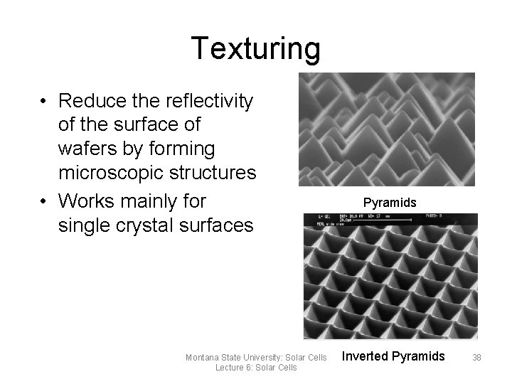
Texturing • Reduce the reflectivity of the surface of wafers by forming microscopic structures • Works mainly for single crystal surfaces Montana State University: Solar Cells Lecture 6: Solar Cells Pyramids Inverted Pyramids 38

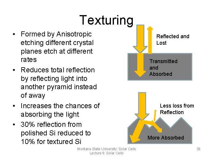
Texturing • Formed by Anisotropic etching different crystal planes etch at different rates • Reduces total reflection by reflecting light into another pyramid instead of away • Increases the chances of absorbing the light • 30% reflection from polished Si reduced to 10% for textured Si Montana State University: Solar Cells Lecture 6: Solar Cells Reflected and Lost Transmitted and Absorbed Less loss from Reflection More Absorbed 39

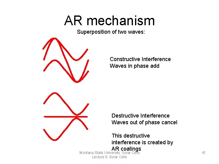
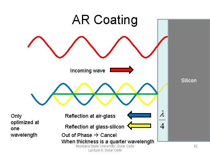
Anti-reflection (AR) Coatings • Finished PV cell is coated with a material to reduce the amount of reflected light (just like eye glasses) • Usually used on cells unsuitable for texturing • Can reduce reflection to 5% • AR Coating Materials – Silicon nitride – Silicon dioxide – Zinc oxide Montana State University: Solar Cells Lecture 6: Solar Cells 40

AR mechanism Superposition of two waves: Constructive Interference Waves in phase add Destructive Interference Waves out of phase cancel This destructive interference is created by AR coatings Montana State University: Solar Cells Lecture 6: Solar Cells 41

AR Coating Incoming wave Silicon Only optimized at one wavelength Reflection at air-glass Reflection at glass-silicon Out of Phase Cancel When thickness is a quarter wavelength Montana State University: Solar Cells Lecture 6: Solar Cells 42

Front Metal Contacts • Grid of metal contacts are used to collect the current from the p-n junction (blocks sunlight to silicon) • Silver is mainly used: Highest conductivity but very expensive (we use aluminum…cheaper) • High conductivity reduces the resistance the traveling electrons experience so they lose less energy as they move • There will be some additional resistance provide by the alloying of the metal and silicon (contact resistance) • A well formed bond minimizes this resistance by allowing electrons to flow between the materials with out any edge effects, barriers or opposing voltages Montana State University: Solar Cells Lecture 6: Solar Cells 43

Front Metal Contacts Process • The main process used by industry is silk-screening because it is quick and cheap – Silver paste is squeezed through a mesh with a pattern onto the cell’s top surface • Other Processes – Evaporation (our method) – Laser Grooving and Electroplating • Slower and more expensive but gives good efficient cells – Inkjet Printing • Fast and cheap in theory • Yet to achieve improved performance Montana State University: Solar Cells Lecture 6: Solar Cells 44

Rear Metal Contacts • Does not need to let sunlight through usually covers the entire back surface • This reduces the back surface contact resistance • Aluminum is usually used for the rear metal contact because a lot is used • Aluminum is a good conductor (not as good as silver) but much less expensive • Made thicker to compensate for lower conductivity Montana State University: Solar Cells Lecture 6: Solar Cells 45

Encapsulation • Solar cells are thin & brittle and need to be exposed to outdoor conditions for 25 -30 years • A physical casing (encapsulation) protects the PV cells and provide structural strength • Accomplishes – Electrically isolate cells and make contacts – Protect from water and oxygen ingress – Withstand heavy winds, hail & installation – Maintain protection for decades – Allow modules to attach to each other Montana State University: Solar Cells Lecture 6: Solar Cells 46

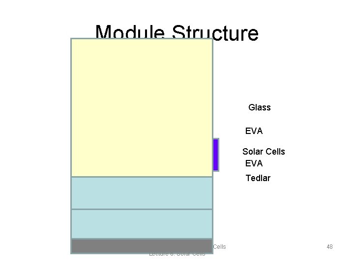
Materials • Glass(low Iron): – Used for the transparent top surface. – Needs to be highly transparent, scratch-resistant & rain, wind, hail, human… proof. • Tedlar – Typical back layer because it is strong material – Gives structural support – Removes excess heat that reduces efficiency • Ethylene Vinyl Acetate (EVA) – Transparent encapsulant – Fills all the spaces between the front, rear edges and between layers Montana State University: Solar Cells Lecture 6: Solar Cells 47

Module Structure Glass EVA Solar Cells EVA Tedlar Montana State University: Solar Cells Lecture 6: Solar Cells 48

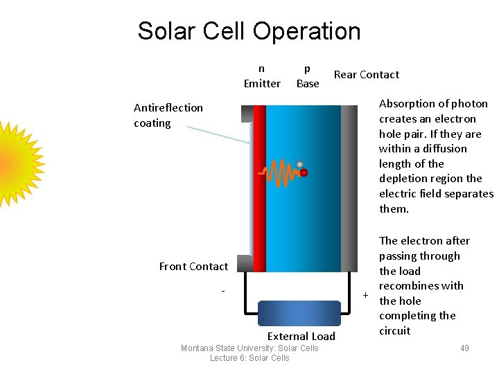
Solar Cell Operation n Emitter p Base Rear Contact Absorption of photon creates an electron hole pair. If they are within a diffusion length of the depletion region the electric field separates them. Antireflection coating Front Contact External Load Montana State University: Solar Cells Lecture 6: Solar Cells The electron after passing through the load recombines with + the hole completing the circuit 49