ECE 3620 Introduction to Microcomputers Wayne State University
- Slides: 49

ECE 3620 Introduction to Microcomputers Wayne State University Electrical and Computer Engineering © 2016, Macam S Dattathreya, Ph. D 1

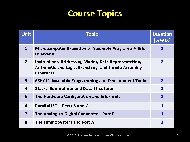
Course Topics Unit Topic Duration (weeks) 1 Microcomputer Execution of Assembly Programs: A Brief Overview 1 2 Instructions, Addressing Modes, Data Representation, Arithmetic and Logic, Branching, and Simple Assembly Programs 2 3 68 HC 11 Assembly Programming and Development Tools 2 4 Stacks, Subroutines and Data Structures 1 5 The Hardware Configuration and Interrupts 1 6 Parallel I/O – Ports B and C 1 7 The Analog-to-Digital Converter – Port E 1 8 The Timing System and Port A 2 © 2016, Macam, Introduction to Microcomputers 2

Unit#7 Table of Contents • • • Port E A/D converter pins (EVBPlus 2 board) A/D converter resolution Configure the A/D system A/D conversion using the 68 HC 11 © 2016, Macam, Introduction to Microcomputers 3

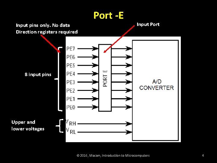
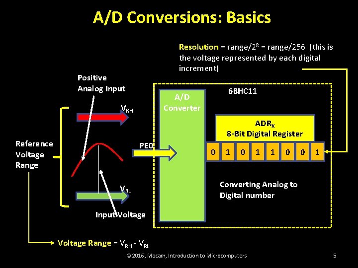
Port -E Input pins only. No data Direction registers required Input Port 8 input pins Upper and lower voltages © 2016, Macam, Introduction to Microcomputers 4

A/D Conversions: Basics Resolution = range/28 = range/256 (this is the voltage represented by each digital increment) Positive Analog Input 68 HC 11 A/D Converter VRH ADRX 8 -Bit Digital Register Reference Voltage Range PE 0 VRL 0 1 1 0 0 1 Converting Analog to Digital number Input Voltage Range = VRH - VRL © 2016, Macam, Introduction to Microcomputers 5

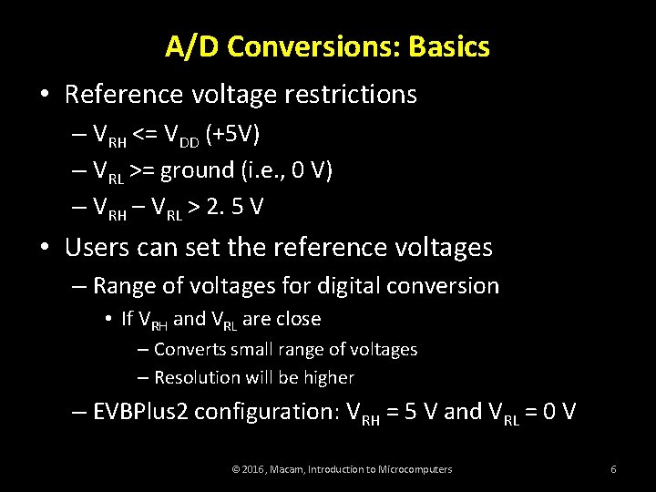
A/D Conversions: Basics • Reference voltage restrictions – VRH <= VDD (+5 V) – VRL >= ground (i. e. , 0 V) – VRH – VRL > 2. 5 V • Users can set the reference voltages – Range of voltages for digital conversion • If VRH and VRL are close – Converts small range of voltages – Resolution will be higher – EVBPlus 2 configuration: VRH = 5 V and VRL = 0 V © 2016, Macam, Introduction to Microcomputers 6

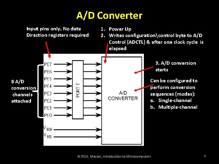
A/D Converter Input pins only. No data Direction registers required 1. Power Up 2. Writes configurationcontrol byte to A/D Control (ADCTL) & after one clock cycle is elapsed 3. A/D conversion starts 8 A/D conversion channels attached Can be configured to perform conversion sequences (modes): a. Single-channel b. Multiple-channel © 2016, Macam, Introduction to Microcomputers 7

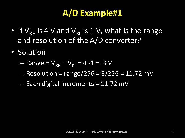
A/D Example#1 • If VRH is 4 V and VRL is 1 V, what is the range and resolution of the A/D converter? • Solution – Range = VRH – VRL = 4 -1 = 3 V – Resolution = range/256 = 3/256 = 11. 72 m. V – Each digital increments = 11. 72 m. V © 2016, Macam, Introduction to Microcomputers 8

A/D Example#2 • An analog input it applied to the A/D converter of the previous example and the digital register reads $49. What is the analog voltage? • Solution – Hex $49 = 7310 • 73 increments of 11. 72 m. V = 0. 85556 V • Add this to VRL or 1 V (to get correct analog voltage) 1. 856 V © 2016, Macam, Introduction to Microcomputers 9

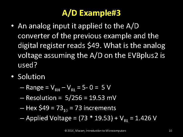
A/D Example#3 • An analog input it applied to the A/D converter of the previous example and the digital register reads $49. What is the analog voltage assuming the A/D on the EVBplus 2 is used? • Solution – Range = VRH – VRL = 5 - 0 = 5 V – Resolution = 5/256 = 19. 53 m. V – Hex $49 = 7310 = 73 increments – Applied Voltage = (73 * 19. 53) + VRL = 1. 426 V © 2016, Macam, Introduction to Microcomputers 10

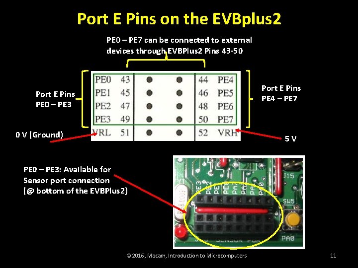
Port E Pins on the EVBplus 2 PE 0 – PE 7 can be connected to external devices through EVBPlus 2 Pins 43 -50 Port E Pins PE 4 – PE 7 Port E Pins PE 0 – PE 3 0 V (Ground) 5 V PE 0 – PE 3: Available for Sensor port connection (@ bottom of the EVBPlus 2) © 2016, Macam, Introduction to Microcomputers 11

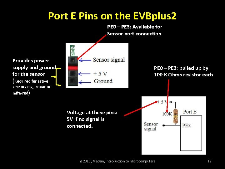
Port E Pins on the EVBplus 2 PE 0 – PE 3: Available for Sensor port connection Provides power supply and ground for the sensor (Required for active PE 0 – PE 3: pulled up by 100 K Ohms resistor each sensors e. g. , sonar or infra-red) Voltage at these pins: 5 V if no signal is connected. © 2016, Macam, Introduction to Microcomputers 12

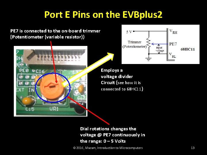
Port E Pins on the EVBplus 2 PE 7 is connected to the on-board trimmer (Potentiometer (variable resistor)) Employs a voltage divider Circuit (see how it is connected to 68 HC 11) Dial rotations changes the voltage @ PE 7 continuously in the range: 0 – 5 Volts © 2016, Macam, Introduction to Microcomputers 13

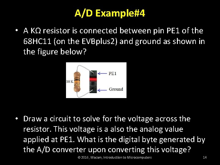
A/D Example#4 • A KΩ resistor is connected between pin PE 1 of the 68 HC 11 (on the EVBplus 2) and ground as shown in the figure below? • Draw a circuit to solve for the voltage across the resistor. This voltage is a also the analog value applied at PE 1. What is the digital byte generated by the A/D converter upon converting this voltage? © 2016, Macam, Introduction to Microcomputers 14

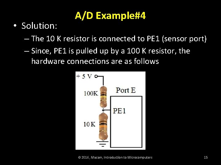
• Solution: A/D Example#4 – The 10 K resistor is connected to PE 1 (sensor port) – Since, PE 1 is pulled up by a 100 K resistor, the hardware connections are as follows © 2016, Macam, Introduction to Microcomputers 15

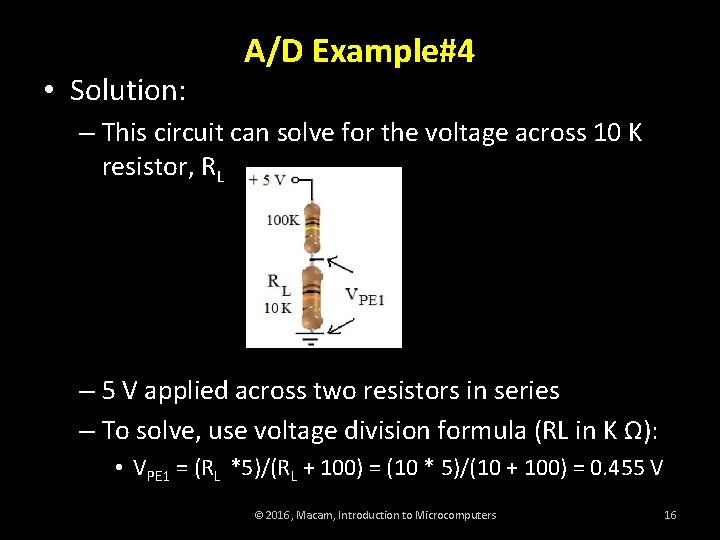
• Solution: A/D Example#4 – This circuit can solve for the voltage across 10 K resistor, RL – 5 V applied across two resistors in series – To solve, use voltage division formula (RL in K Ω): • VPE 1 = (RL *5)/(RL + 100) = (10 * 5)/(10 + 100) = 0. 455 V © 2016, Macam, Introduction to Microcomputers 16

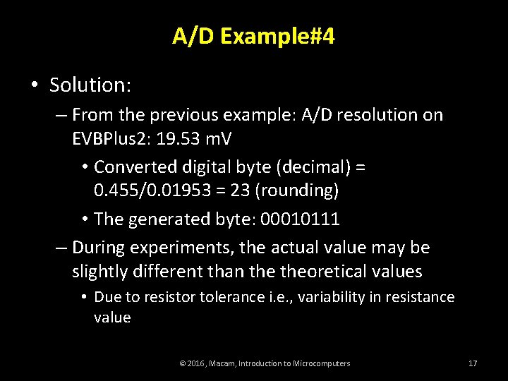
A/D Example#4 • Solution: – From the previous example: A/D resolution on EVBPlus 2: 19. 53 m. V • Converted digital byte (decimal) = 0. 455/0. 01953 = 23 (rounding) • The generated byte: 00010111 – During experiments, the actual value may be slightly different than theoretical values • Due to resistor tolerance i. e. , variability in resistance value © 2016, Macam, Introduction to Microcomputers 17

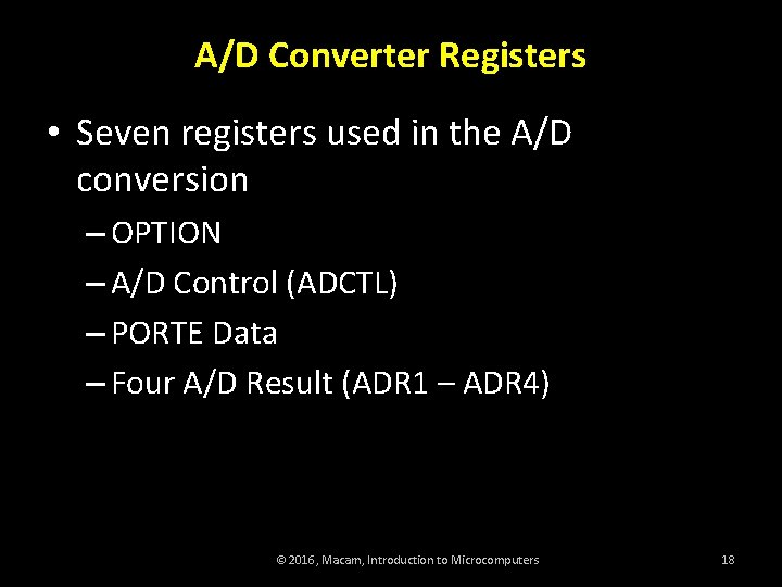
A/D Converter Registers • Seven registers used in the A/D conversion – OPTION – A/D Control (ADCTL) – PORTE Data – Four A/D Result (ADR 1 – ADR 4) © 2016, Macam, Introduction to Microcomputers 18

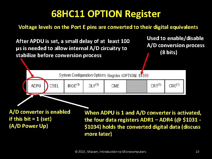
68 HC 11 OPTION Register Voltage levels on the Port E pins are converted to their digital equivalents After APDU is set, a small delay of at least 100 µs is needed to allow internal A/D circuitry to stabilize before conversion process A/D converter is enabled if this bit = 1 (set) (A/D Power Up) Used to enable/disable A/D conversion process (8 bits) When ADPU is 1 and A/D converter is activated, the four data registers ADR 1 – ADR 4 (@ $1031 $1034) holds the converted digital data (discuss more later) © 2016, Macam, Introduction to Microcomputers 19

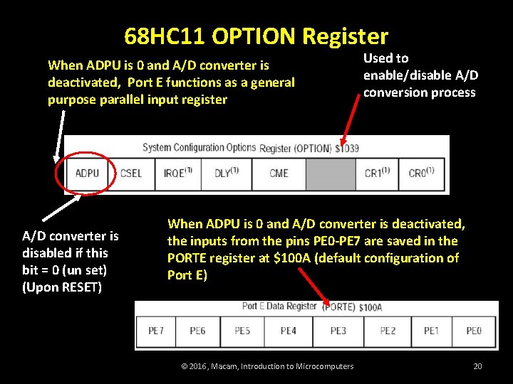
68 HC 11 OPTION Register When ADPU is 0 and A/D converter is deactivated, Port E functions as a general purpose parallel input register A/D converter is disabled if this bit = 0 (un set) (Upon RESET) Used to enable/disable A/D conversion process When ADPU is 0 and A/D converter is deactivated, the inputs from the pins PE 0 -PE 7 are saved in the PORTE register at $100 A (default configuration of Port E) © 2016, Macam, Introduction to Microcomputers 20

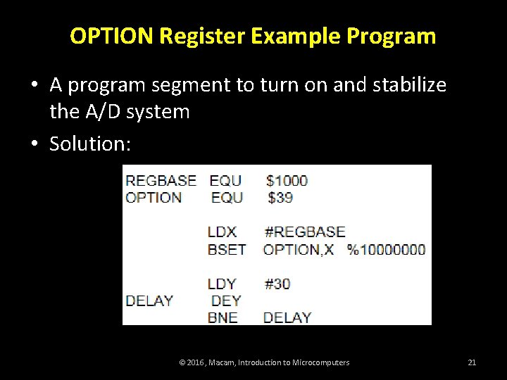
OPTION Register Example Program • A program segment to turn on and stabilize the A/D system • Solution: © 2016, Macam, Introduction to Microcomputers 21

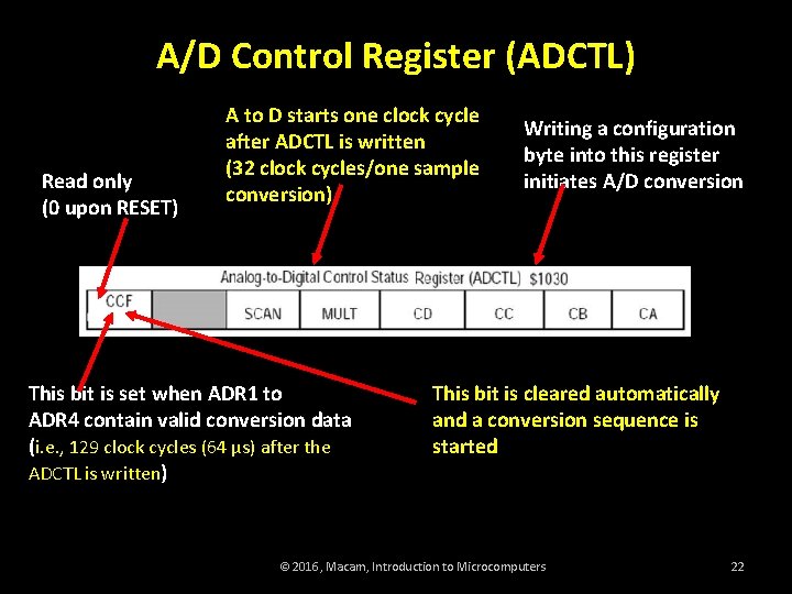
A/D Control Register (ADCTL) Read only (0 upon RESET) A to D starts one clock cycle after ADCTL is written (32 clock cycles/one sample conversion) This bit is set when ADR 1 to ADR 4 contain valid conversion data (i. e. , 129 clock cycles (64 µs) after the ADCTL is written) Writing a configuration byte into this register initiates A/D conversion This bit is cleared automatically and a conversion sequence is started © 2016, Macam, Introduction to Microcomputers 22

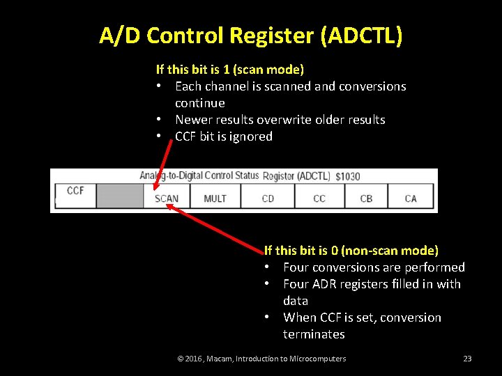
A/D Control Register (ADCTL) If this bit is 1 (scan mode) • Each channel is scanned and conversions continue • Newer results overwrite older results • CCF bit is ignored If this bit is 0 (non-scan mode) • Four conversions are performed • Four ADR registers filled in with data • When CCF is set, conversion terminates © 2016, Macam, Introduction to Microcomputers 23

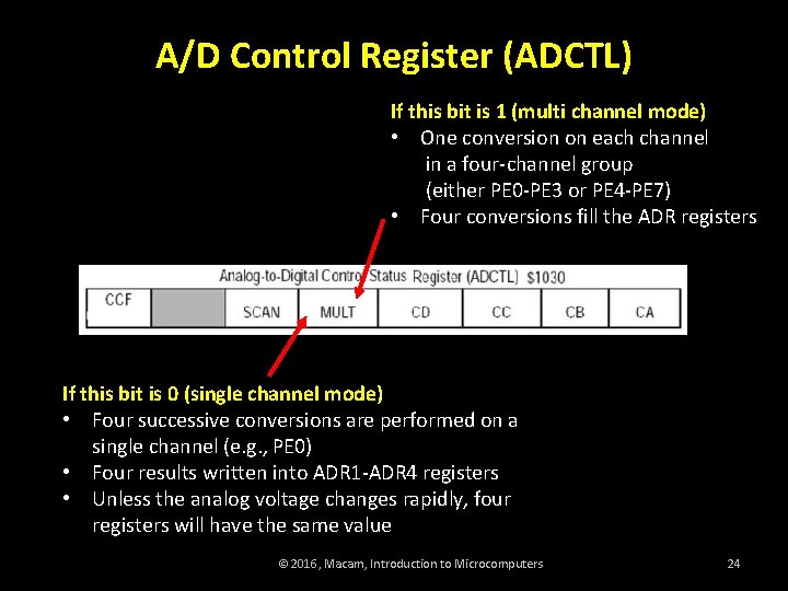
A/D Control Register (ADCTL) If this bit is 1 (multi channel mode) • One conversion on each channel in a four-channel group (either PE 0 -PE 3 or PE 4 -PE 7) • Four conversions fill the ADR registers If this bit is 0 (single channel mode) • Four successive conversions are performed on a single channel (e. g. , PE 0) • Four results written into ADR 1 -ADR 4 registers • Unless the analog voltage changes rapidly, four registers will have the same value © 2016, Macam, Introduction to Microcomputers 24

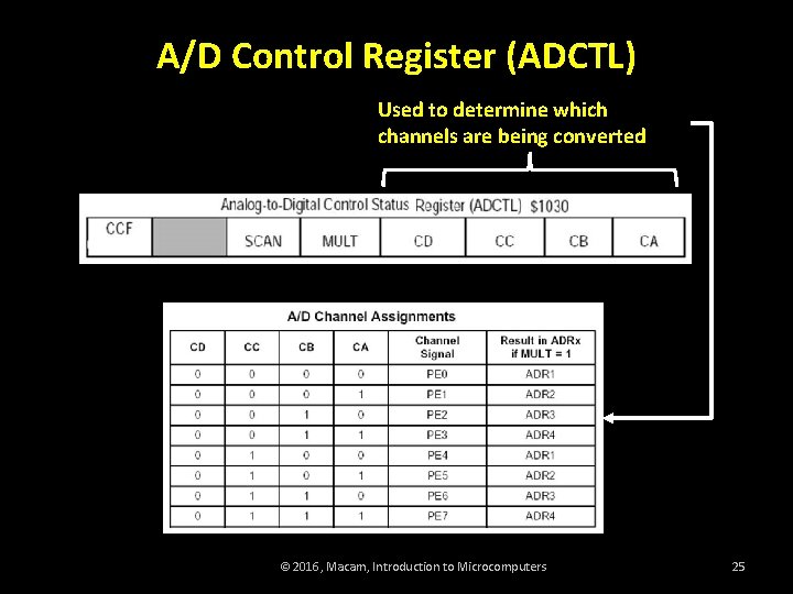
A/D Control Register (ADCTL) Used to determine which channels are being converted © 2016, Macam, Introduction to Microcomputers 25

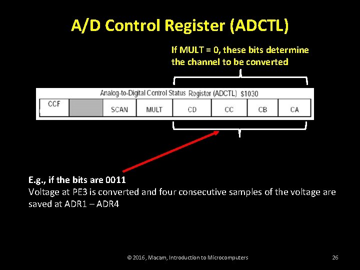
A/D Control Register (ADCTL) If MULT = 0, these bits determine the channel to be converted E. g. , if the bits are 0011 Voltage at PE 3 is converted and four consecutive samples of the voltage are saved at ADR 1 – ADR 4 © 2016, Macam, Introduction to Microcomputers 26

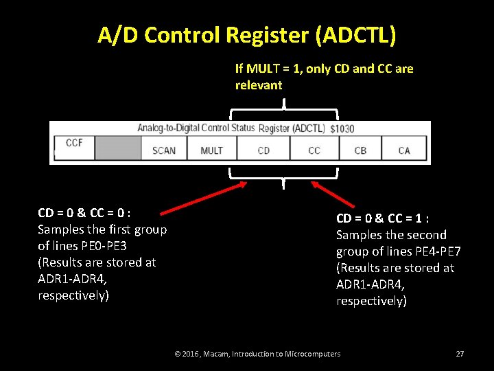
A/D Control Register (ADCTL) If MULT = 1, only CD and CC are relevant CD = 0 & CC = 0 : Samples the first group of lines PE 0 -PE 3 (Results are stored at ADR 1 -ADR 4, respectively) CD = 0 & CC = 1 : Samples the second group of lines PE 4 -PE 7 (Results are stored at ADR 1 -ADR 4, respectively) © 2016, Macam, Introduction to Microcomputers 27

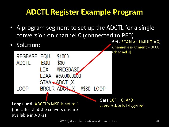
ADCTL Register Example Program • A program segment to set up the ADCTL for a single conversion on channel 0 (connected to PE 0) Sets SCAN and MULT = 0; • Solution: Channel assignment = 0000 (channel 0) Loops until ADCTL’s MSB is set to 1 (indicates that the conversions are available in ADRs) Sets CCF = 0; A/D conversion is triggered © 2016, Macam, Introduction to Microcomputers 28

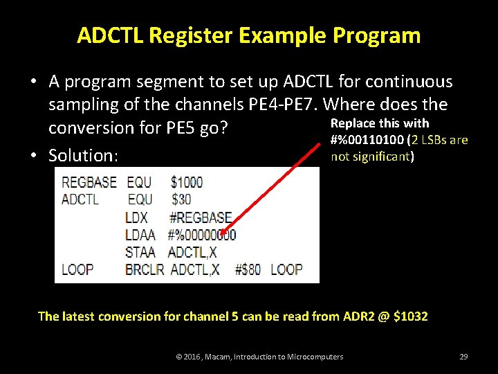
ADCTL Register Example Program • A program segment to set up ADCTL for continuous sampling of the channels PE 4 -PE 7. Where does the Replace this with conversion for PE 5 go? #%00110100 (2 LSBs are not significant) • Solution: The latest conversion for channel 5 can be read from ADR 2 @ $1032 © 2016, Macam, Introduction to Microcomputers 29

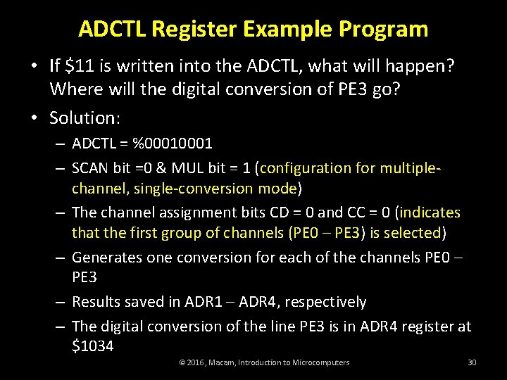
ADCTL Register Example Program • If $11 is written into the ADCTL, what will happen? Where will the digital conversion of PE 3 go? • Solution: – ADCTL = %0001 – SCAN bit =0 & MUL bit = 1 (configuration for multiplechannel, single-conversion mode) – The channel assignment bits CD = 0 and CC = 0 (indicates that the first group of channels (PE 0 – PE 3) is selected) – Generates one conversion for each of the channels PE 0 – PE 3 – Results saved in ADR 1 – ADR 4, respectively – The digital conversion of the line PE 3 is in ADR 4 register at $1034 © 2016, Macam, Introduction to Microcomputers 30

ADCTL Register Programing Example 1 • A program segment to set up the ADCTL for a single conversion on channel 5 (connected to PE 5). Send the converted result to PORTB. Make sure you include code to activate the A/D converter • Solution: © 2016, Macam, Introduction to Microcomputers 31

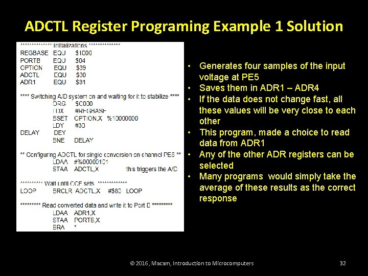
ADCTL Register Programing Example 1 Solution • Generates four samples of the input voltage at PE 5 • Saves them in ADR 1 – ADR 4 • If the data does not change fast, all these values will be very close to each other • This program, made a choice to read data from ADR 1 • Any of the other ADR registers can be selected • Many programs would simply take the average of these results as the correct response © 2016, Macam, Introduction to Microcomputers 32

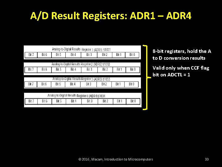
A/D Result Registers: ADR 1 – ADR 4 8 -bit registers, hold the A to D conversion results Valid only when CCF flag bit on ADCTL = 1 © 2016, Macam, Introduction to Microcomputers 33

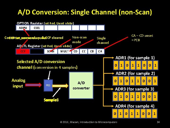
A/D Conversion: Single Channel (non-Scan) OPTION Register (set Red, Unset white) ADPU CSEL Converter upover & CCF cleared CCF set, powered conversion ADCTL Register (set Red, Unset white) CCF SCAN MULT Non-scan mode CD CC Selected A/D conversion channel (conversion in 4 samples) CA – CD unset = PE 0 Single channel CB CA ADR 1 (for sample 1) 0 1 1 0 0 1 ADR 2 (for sample 2) Analog input PE 0 Sample 4 Sample 2 Sample 1 Sample 3 A/D converter 0 1 1 0 0 1 ADR 3 (for sample 3) 0 1 1 0 0 1 ADR 4 (for sample 4) 0 1 1 0 0 1 © 2016, Macam, Introduction to Microcomputers 34

A/D Conversion: Single Channel (non-Scan) • Single-channel mode (on selected channel): – Can be configured to perform conversion sequences four times – Non-scan and scan-modes • Non-scan: Four consecutive samples from the single selected channel and converted • First result stored in ADR 1, second in ADR 2, etc. • After fourth conversion is completed, conversion halts • Conversion command written to ADCTL © 2016, Macam, Introduction to Microcomputers 35

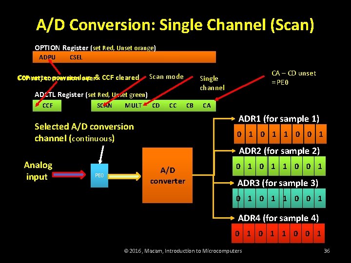
A/D Conversion: Single Channel (Scan) OPTION Register (set Red, Unset orange) ADPU CSEL Converter powered over up & CCF cleared CCF set, conversion Scan mode ADCTL Register (set Red, Unset green) CCF SCAN MULT CD CC CA – CD unset = PE 0 Single channel CB CA ADR 1 (for sample 1) Selected A/D conversion channel (continuous) 0 1 1 0 0 1 ADR 2 (for sample 2) Analog input PE 0 A/D converter 0 1 1 0 0 1 ADR 3 (for sample 3) 0 1 1 0 0 1 ADR 4 (for sample 4) 0 1 1 0 0 1 © 2016, Macam, Introduction to Microcomputers 36

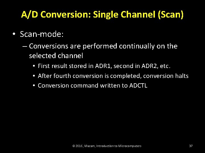
A/D Conversion: Single Channel (Scan) • Scan-mode: – Conversions are performed continually on the selected channel • First result stored in ADR 1, second in ADR 2, etc. • After fourth conversion is completed, conversion halts • Conversion command written to ADCTL © 2016, Macam, Introduction to Microcomputers 37

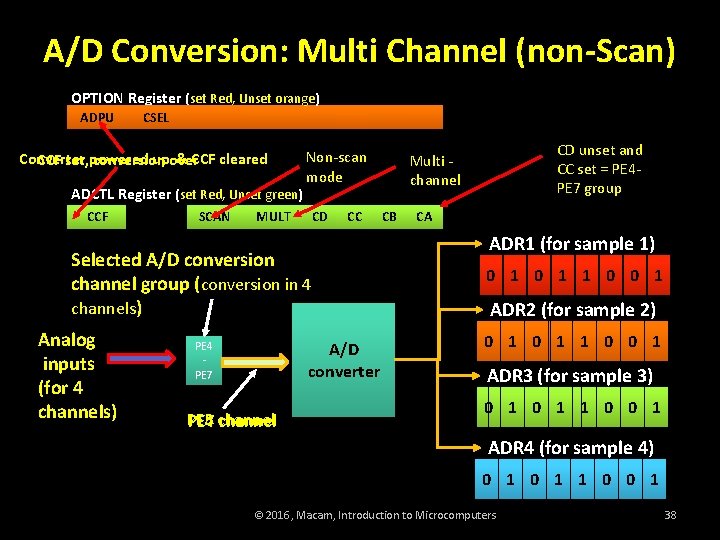
A/D Conversion: Multi Channel (non-Scan) OPTION Register (set Red, Unset orange) ADPU CSEL Converter upover & CCF cleared CCF set, powered conversion ADCTL Register (set Red, Unset green) CCF MULT SCAN Non-scan mode MULT CD CC Selected A/D conversion channel group (conversion in 4 channels) Analog inputs (for 4 channels) A/D converter PE 4 PE 7 PE 5 PE 6 PE 7 channel PE 4 CD unset and CC set = PE 4 PE 7 group Multi channel CB CA ADR 1 (for sample 1) 0 1 1 0 0 1 ADR 2 (for sample 2) 0 1 1 0 0 1 ADR 3 (for sample 3) 0 1 1 0 0 1 ADR 4 (for sample 4) 0 1 1 0 0 1 © 2016, Macam, Introduction to Microcomputers 38

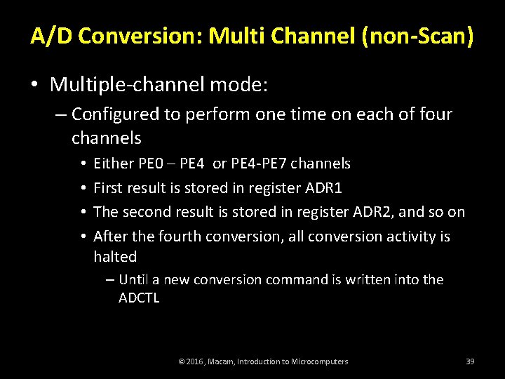
A/D Conversion: Multi Channel (non-Scan) • Multiple-channel mode: – Configured to perform one time on each of four channels • • Either PE 0 – PE 4 or PE 4 -PE 7 channels First result is stored in register ADR 1 The second result is stored in register ADR 2, and so on After the fourth conversion, all conversion activity is halted – Until a new conversion command is written into the ADCTL © 2016, Macam, Introduction to Microcomputers 39

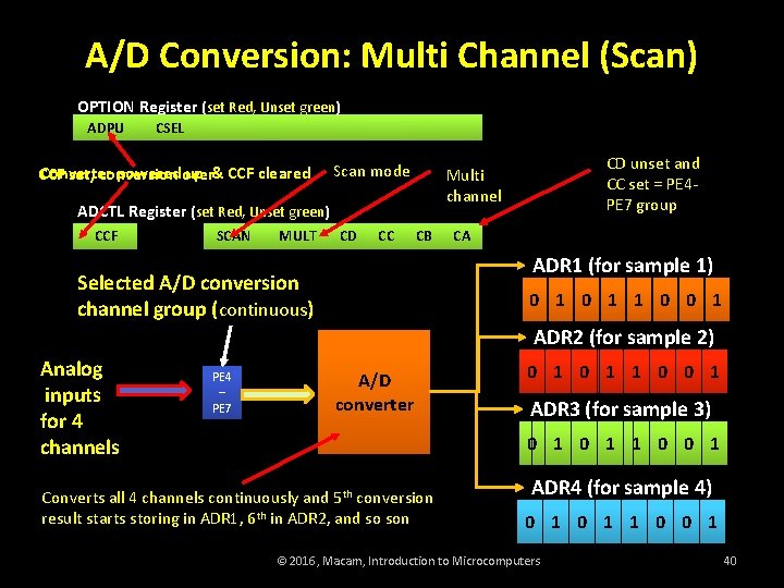
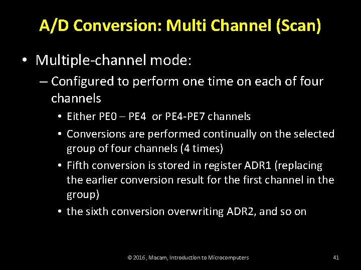
A/D Conversion: Multi Channel (Scan) OPTION Register (set Red, Unset green) ADPU CSEL Converter powered over up & CCF cleared CCF set, conversion Scan mode ADCTL Register (set Red, Unset green) CCF MULT SCAN MULT CD CC CD unset and CC set = PE 4 PE 7 group Multi channel CB CA ADR 1 (for sample 1) Selected A/D conversion channel group (continuous) 0 1 1 0 0 1 ADR 2 (for sample 2) Analog inputs for 4 channels PE 4 – PE 7 A/D converter 0 1 1 0 0 1 ADR 3 (for sample 3) 0 1 1 0 0 1 Converts all 4 channels continuously and 5 th conversion result starts storing in ADR 1, 6 th in ADR 2, and so son ADR 4 (for sample 4) 0 1 1 0 0 1 © 2016, Macam, Introduction to Microcomputers 40

A/D Conversion: Multi Channel (Scan) • Multiple-channel mode: – Configured to perform one time on each of four channels • Either PE 0 – PE 4 or PE 4 -PE 7 channels • Conversions are performed continually on the selected group of four channels (4 times) • Fifth conversion is stored in register ADR 1 (replacing the earlier conversion result for the first channel in the group) • the sixth conversion overwriting ADR 2, and so on © 2016, Macam, Introduction to Microcomputers 41

Procedure for Using A/D System • Step 1: – Connect the hardware properly – Input analog voltage range between VRH - VRL – Else, must scale the input signal and bias it to the proper range. If EVBplus 2: range = 0 to 5 V • Step 2: – Set the ADPU bit of the OPTION register to enable the A/D system © 2016, Macam, Introduction to Microcomputers 42

Procedure for Using A/D System • Step 3: – Wait for the A/D system to stabilize – The user can use a program loop to create a delay of at least 100 ms • Step 4: – Select the appropriate channel(s) and operation modes by programming the ADCTL register © 2016, Macam, Introduction to Microcomputers 43

Procedure for Using A/D System • Step 5: – Non-scan mode: • Wait until the CCF bit (ADCTL) is set • Then collect the A/D conversion results and use them in your program • When CCF bit is 1, the ADCTL value becomes negative, user to decide if the conversion is completed • While CCF = 1, no further conversions are performed • When CCF = 0, A new conversion is automatically performed – Scan-Mode: • Conversions are continuous, no waiting for CCF bit set © 2016, Macam, Introduction to Microcomputers 44

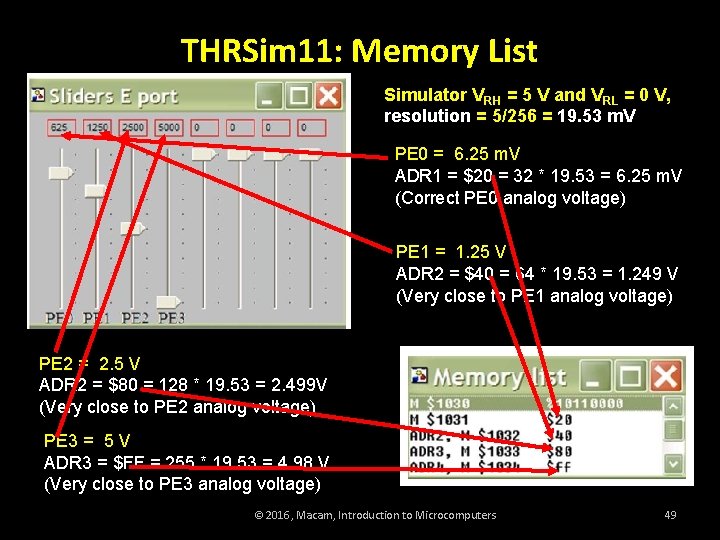
ADCTL Register Programing Example 2 • Write a program to set up the ADCTL for continuous conversion of channels PE 0 -PE 3. Run the program on the THRSim 11. Employ the “Slider E port” tool to provides the following input voltages: 625 m. V on PE 0, 1. 25 V on PE 1, 2. 5 V on PE 2 and 5 V on PE 3. Run the program and verify the contents of the ADCTL register ($1030) and the ADR 1 – ADR 4 registers ($1031 - $1034). • Solution: © 2016, Macam, Introduction to Microcomputers 45

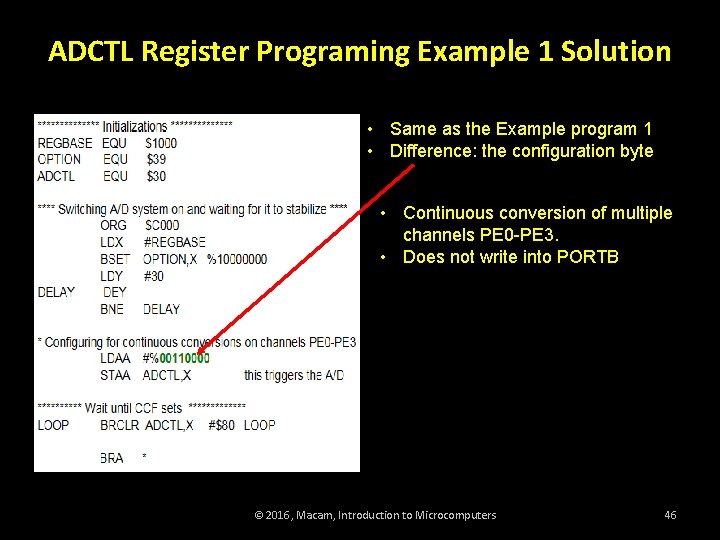
ADCTL Register Programing Example 1 Solution • Same as the Example program 1 • Difference: the configuration byte • Continuous conversion of multiple channels PE 0 -PE 3. • Does not write into PORTB © 2016, Macam, Introduction to Microcomputers 46

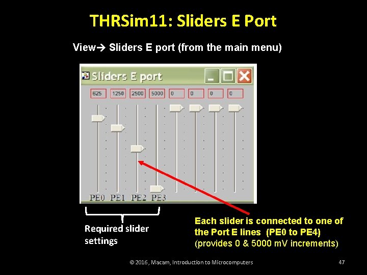
THRSim 11: Sliders E Port View Sliders E port (from the main menu) Required slider settings Each slider is connected to one of the Port E lines (PE 0 to PE 4) (provides 0 & 5000 m. V increments) © 2016, Macam, Introduction to Microcomputers 47

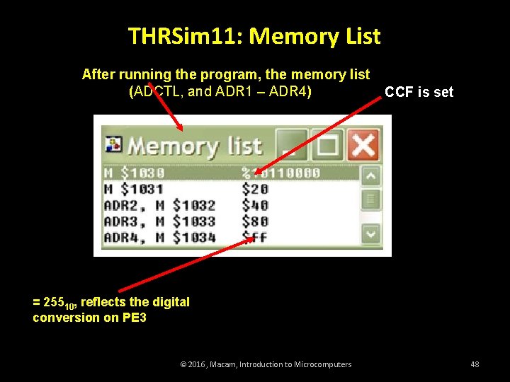
THRSim 11: Memory List After running the program, the memory list (ADCTL, and ADR 1 – ADR 4) CCF is set = 25510, reflects the digital conversion on PE 3 © 2016, Macam, Introduction to Microcomputers 48

THRSim 11: Memory List Simulator VRH = 5 V and VRL = 0 V, resolution = 5/256 = 19. 53 m. V PE 0 = 6. 25 m. V ADR 1 = $20 = 32 * 19. 53 = 6. 25 m. V (Correct PE 0 analog voltage) PE 1 = 1. 25 V ADR 2 = $40 = 64 * 19. 53 = 1. 249 V (Very close to PE 1 analog voltage) PE 2 = 2. 5 V ADR 2 = $80 = 128 * 19. 53 = 2. 499 V (Very close to PE 2 analog voltage) PE 3 = 5 V ADR 3 = $FF = 255 * 19. 53 = 4. 98 V (Very close to PE 3 analog voltage) © 2016, Macam, Introduction to Microcomputers 49