ECE 353 Introduction to Microprocessor Systems Week 8



![001 D C 7 07 1234 mov [bx], 1234 h 001 D C 7 07 1234 mov [bx], 1234 h](https://slidetodoc.com/presentation_image_h2/09408a8fe2b030cb53cd69aced84bd32/image-24.jpg)
![0021 8 A 07 mov al, [bx] 0021 8 A 07 mov al, [bx]](https://slidetodoc.com/presentation_image_h2/09408a8fe2b030cb53cd69aced84bd32/image-25.jpg)
- Slides: 28

ECE 353 Introduction to Microprocessor Systems Week 8 Michael G. Morrow, P. E.

Intel Information Session Wednesday, October 24 th 4: 00 PM – 5: 30 PM Memorial Union, Refer to ‘TITU’ for Location Engineering students are invited to attend and learn about exciting full-time and intern opportunities at Intel. Refreshments will be provided. Intel now accepts resumes online at: www. intel. com/jobs/resume Casual attire is appropriate for all our campus events! We offer internships and full time positions in Washington, Oregon, New Mexico, Arizona, Massachusetts, Colorado, and Northern and Southern California.

Intel Open Forum Mike Splinter, Intel Executive VP Director of Sales and Marketing Friday, October 26 th 11: 30 AM – 1: 00 PM Union South, Refer to ‘TITU’ for Location All Students invited to come and hear about Intel’s current direction and future strategies from a top leader within the company. Questions are encouraged! Biography: Mike is a graduate of the University of Wisconsin, earning both bachelor and master degrees in Electrical Engineering in 1972 and 1974, respectively. Mike joined Intel in 1984 as a Fabrication Manager. He has held various management positions within the company, most notable as Assistant General Manager of the Technology Manufacturing Group and as Executive Vice President and General Manager of the Technology and Manufacturing Group. He was promoted to Senior Vice President in January 1999. He holds two Rockwell patents: one for the quarter micron transistor process, and the other for microwave annealing of implanted junctions.

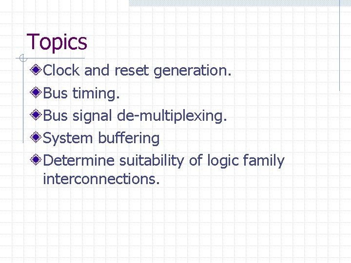
Topics Clock and reset generation. Bus timing. Bus signal de-multiplexing. System buffering Determine suitability of logic family interconnections.

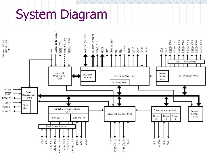
System Diagram

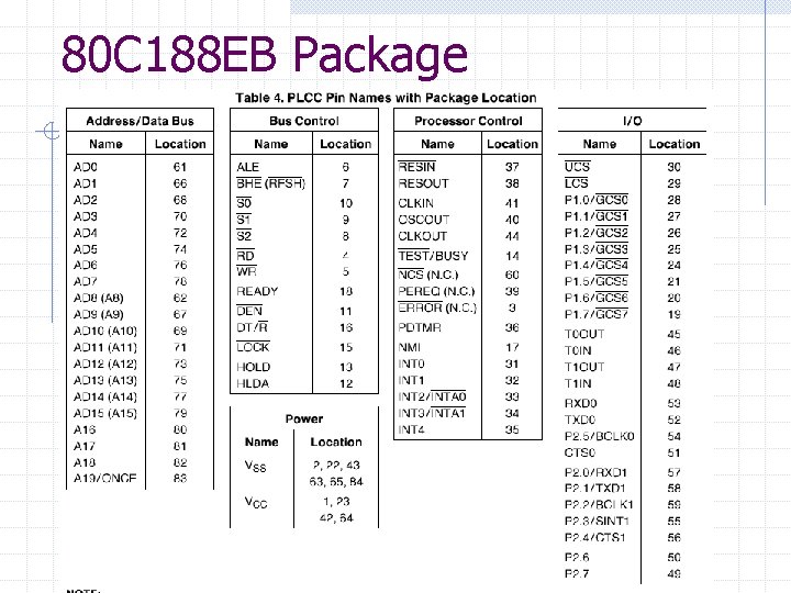
80 C 188 EB Package

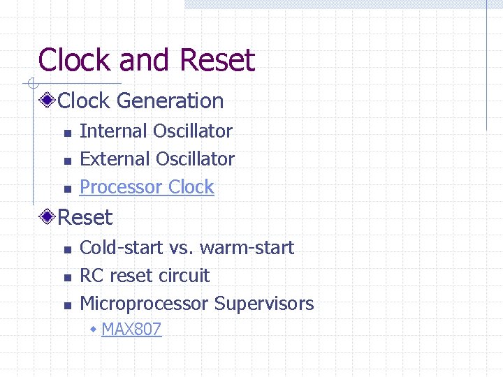
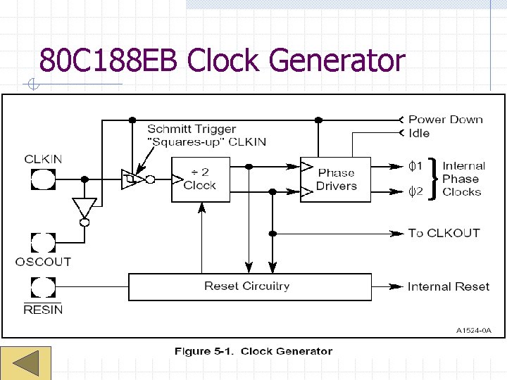
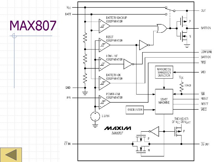
Clock and Reset Clock Generation n Internal Oscillator External Oscillator Processor Clock Reset n n n Cold-start vs. warm-start RC reset circuit Microprocessor Supervisors w MAX 807

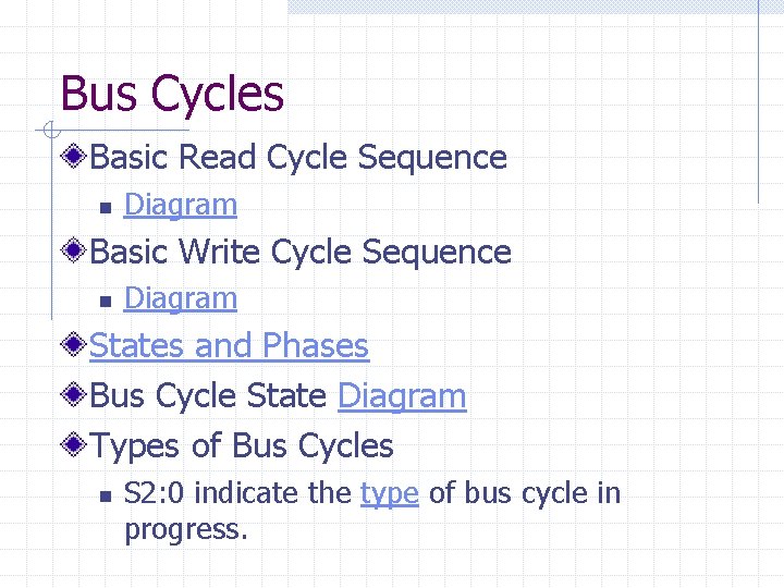
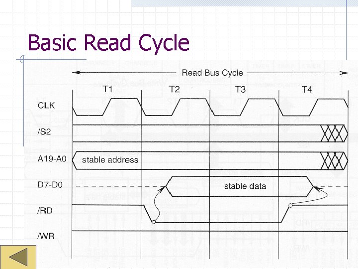
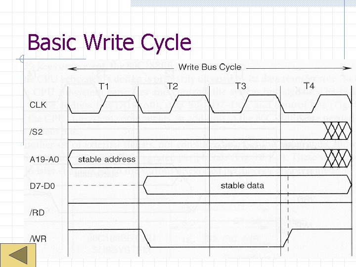
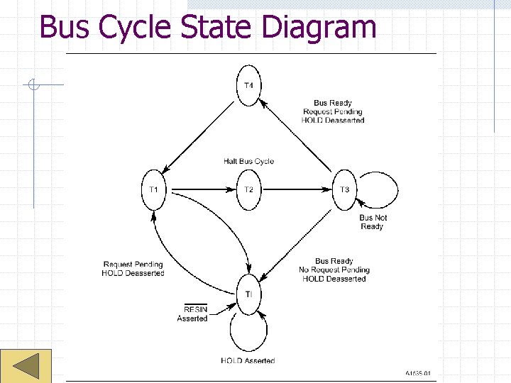
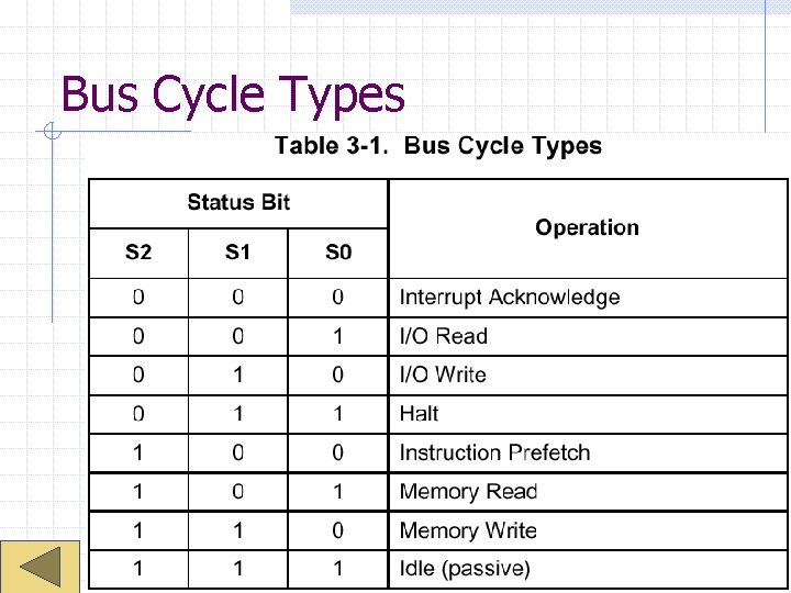
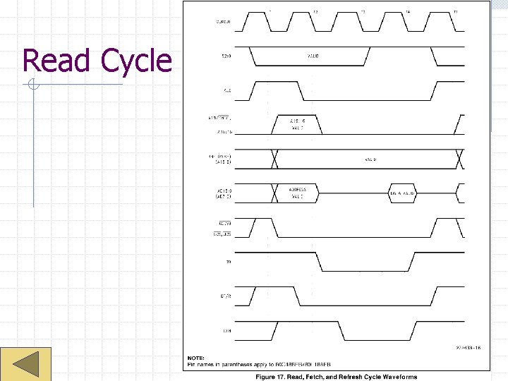
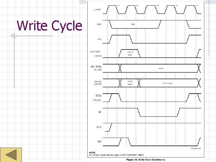
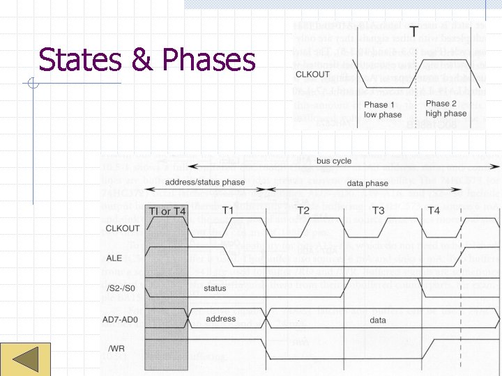
Bus Cycles Basic Read Cycle Sequence n Diagram Basic Write Cycle Sequence n Diagram States and Phases Bus Cycle State Diagram Types of Bus Cycles n S 2: 0 indicate the type of bus cycle in progress.

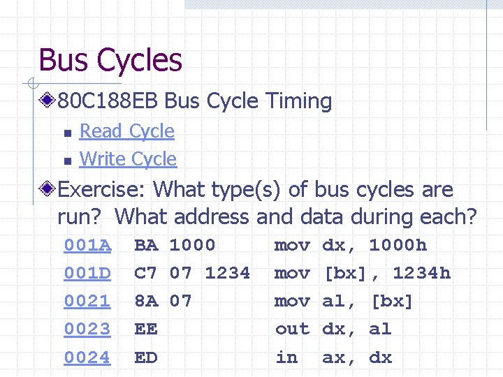
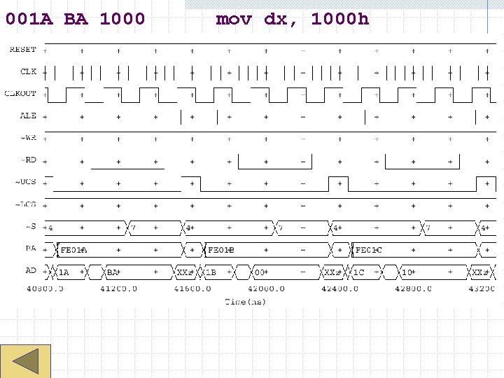
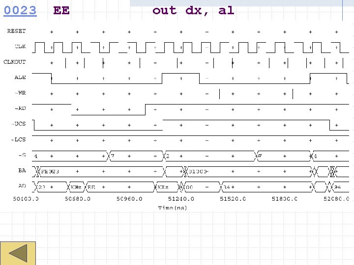
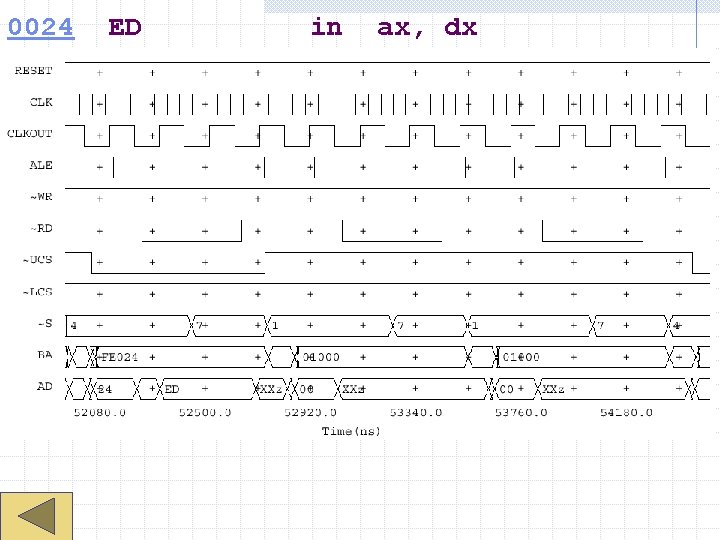
Bus Cycles 80 C 188 EB Bus Cycle Timing n n Read Cycle Write Cycle Exercise: What type(s) of bus cycles are run? What address and data during each? 001 A 001 D 0021 0023 0024 BA 1000 C 7 07 1234 8 A 07 EE ED mov mov out in dx, 1000 h [bx], 1234 h al, [bx] dx, al ax, dx

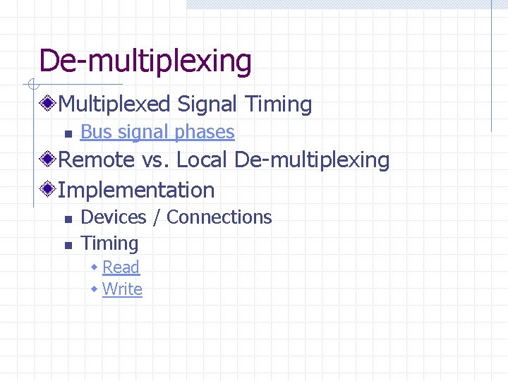
De-multiplexing Multiplexed Signal Timing n Bus signal phases Remote vs. Local De-multiplexing Implementation n n Devices / Connections Timing w Read w Write

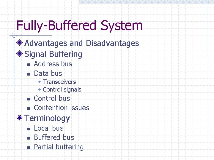
Fully-Buffered System Advantages and Disadvantages Signal Buffering n n Address bus Data bus w Transceivers w Control signals n n Control bus Contention issues Terminology n n n Local bus Buffered bus Partial buffering

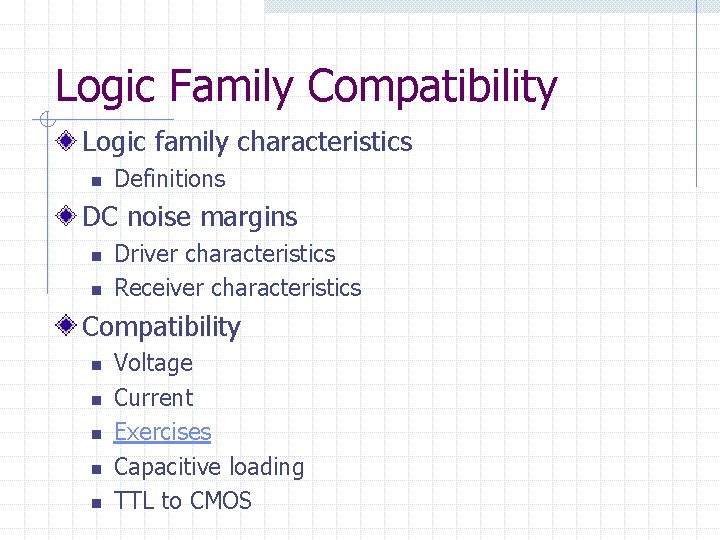
Logic Family Compatibility Logic family characteristics n Definitions DC noise margins n n Driver characteristics Receiver characteristics Compatibility n n n Voltage Current Exercises Capacitive loading TTL to CMOS

Wrapping Up Homework #4 due Friday, 10/26/2001

80 C 188 EB Clock Generator

MAX 807

Basic Read Cycle

Basic Write Cycle

Bus Cycle State Diagram

Bus Cycle Types

Read Cycle

Write Cycle

States & Phases

001 A BA 1000 mov dx, 1000 h
![001 D C 7 07 1234 mov bx 1234 h 001 D C 7 07 1234 mov [bx], 1234 h](https://slidetodoc.com/presentation_image_h2/09408a8fe2b030cb53cd69aced84bd32/image-24.jpg)
001 D C 7 07 1234 mov [bx], 1234 h
![0021 8 A 07 mov al bx 0021 8 A 07 mov al, [bx]](https://slidetodoc.com/presentation_image_h2/09408a8fe2b030cb53cd69aced84bd32/image-25.jpg)
0021 8 A 07 mov al, [bx]

0023 EE out dx, al

0024 ED in ax, dx

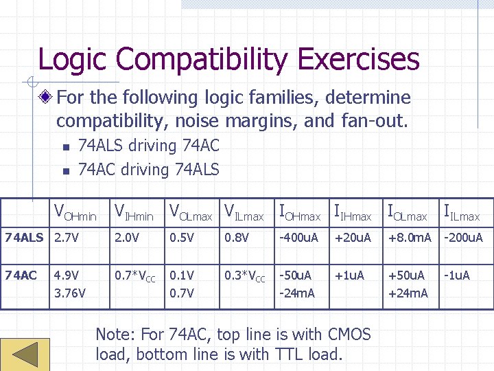
Logic Compatibility Exercises For the following logic families, determine compatibility, noise margins, and fan-out. n n 74 ALS driving 74 AC driving 74 ALS VOHmin VIHmin VOLmax VILmax IOHmax IIHmax IOLmax IILmax 74 ALS 2. 7 V 2. 0 V 0. 5 V 0. 8 V -400 u. A +20 u. A +8. 0 m. A -200 u. A 74 AC 0. 7*VCC 0. 1 V 0. 7 V 0. 3*VCC -50 u. A -24 m. A +1 u. A +50 u. A +24 m. A 4. 9 V 3. 76 V Note: For 74 AC, top line is with CMOS load, bottom line is with TTL load. -1 u. A