ECE 353 Introduction to Microprocessor Systems Week 10

- Slides: 39

ECE 353 Introduction to Microprocessor Systems Week 10 Michael G. Morrow, P. E.

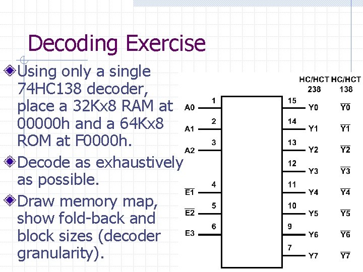
Decoding Exercise Using only a single 74 HC 138 decoder, place a 32 Kx 8 RAM at 00000 h and a 64 Kx 8 ROM at F 0000 h. Decode as exhaustively as possible. Draw memory map, show fold-back and block sizes (decoder granularity).

Topics I/O port basics I/O ports with MSI devices P compatible devices Address decoding for isolated and memory-mapped I/O Conditional I/O 80 C 188 EB integrated I/O unit 82 C 55 A PPI

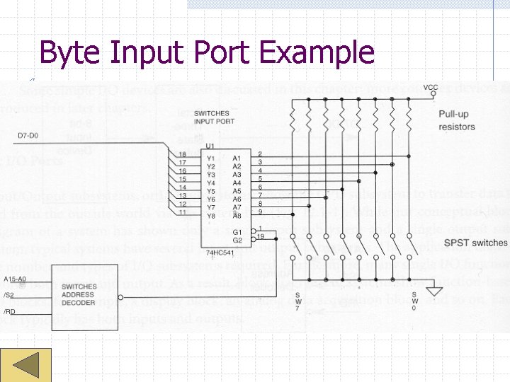
I/O Port Basics I/O subsystems allow CPU to interact with the outside world Input, output, and combined I/O blocks Input ports n n Byte Word Output ports n Byte Unconditional I/O

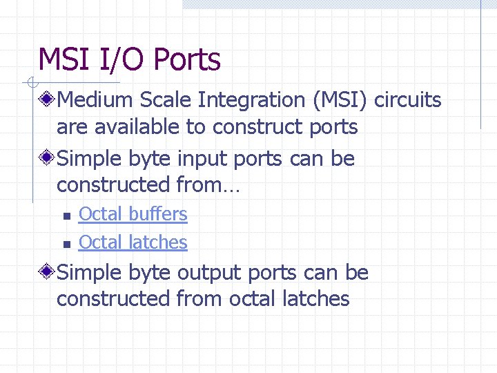
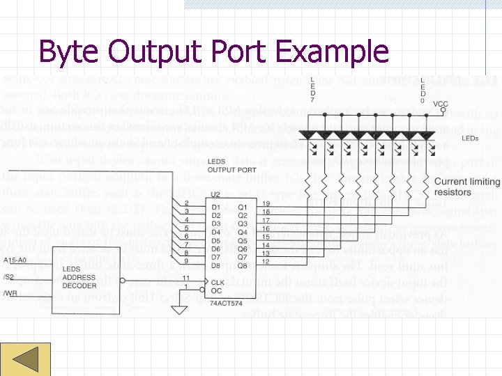
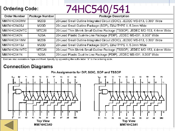
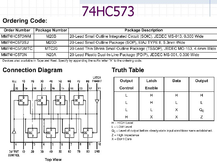
MSI I/O Ports Medium Scale Integration (MSI) circuits are available to construct ports Simple byte input ports can be constructed from… n n Octal buffers Octal latches Simple byte output ports can be constructed from octal latches

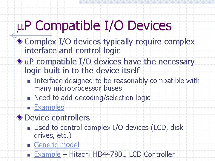
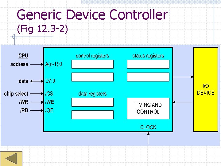
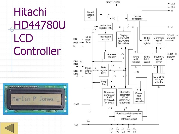
P Compatible I/O Devices Complex I/O devices typically require complex interface and control logic P compatible I/O devices have the necessary logic built in to the device itself n n n Interface designed to be reasonably compatible with many microprocessor buses Need to add decoding/selection logic Examples Device controllers n n n Used to control complex I/O devices (LCD, disk drives, etc. ) Generic model Example – Hitachi HD 44780 U LCD Controller

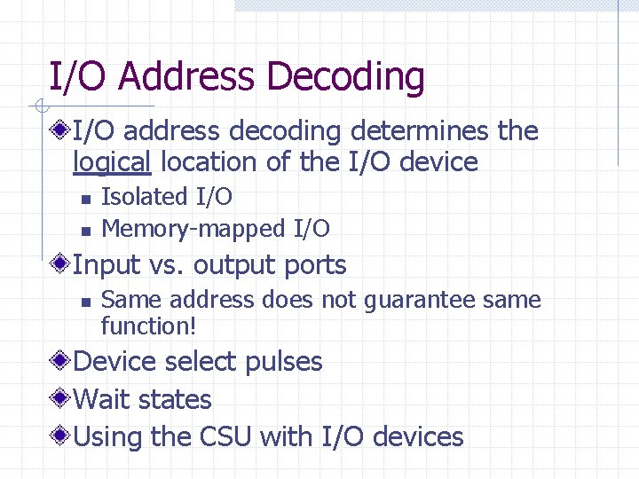
I/O Address Decoding I/O address decoding determines the logical location of the I/O device n n Isolated I/O Memory-mapped I/O Input vs. output ports n Same address does not guarantee same function! Device select pulses Wait states Using the CSU with I/O devices

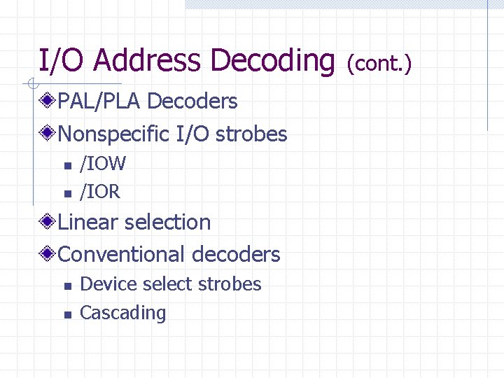
I/O Address Decoding PAL/PLA Decoders Nonspecific I/O strobes n n /IOW /IOR Linear selection Conventional decoders n n Device select strobes Cascading (cont. )

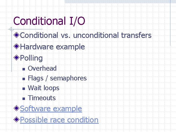
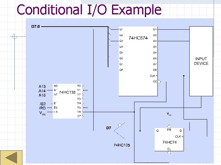
Conditional I/O Conditional vs. unconditional transfers Hardware example Polling n n Overhead Flags / semaphores Wait loops Timeouts Software example Possible race condition

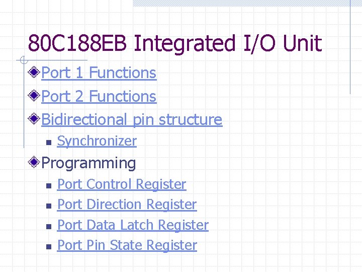
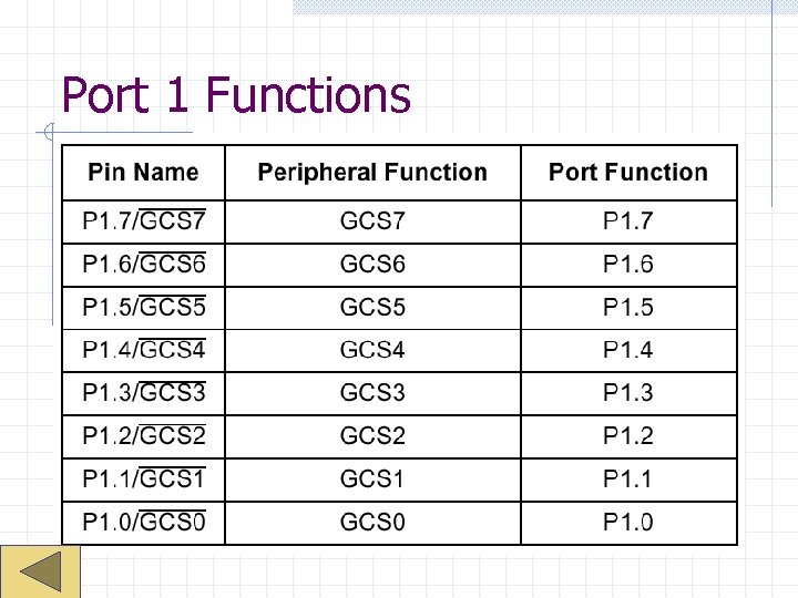
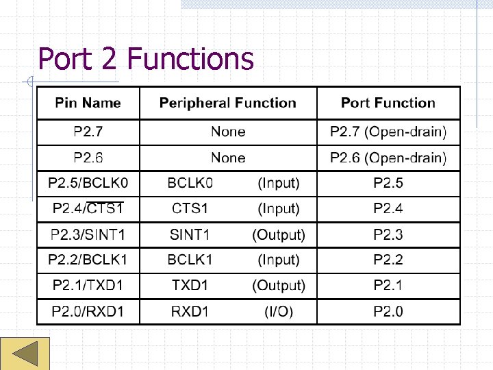
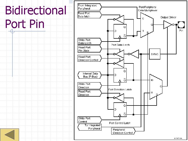
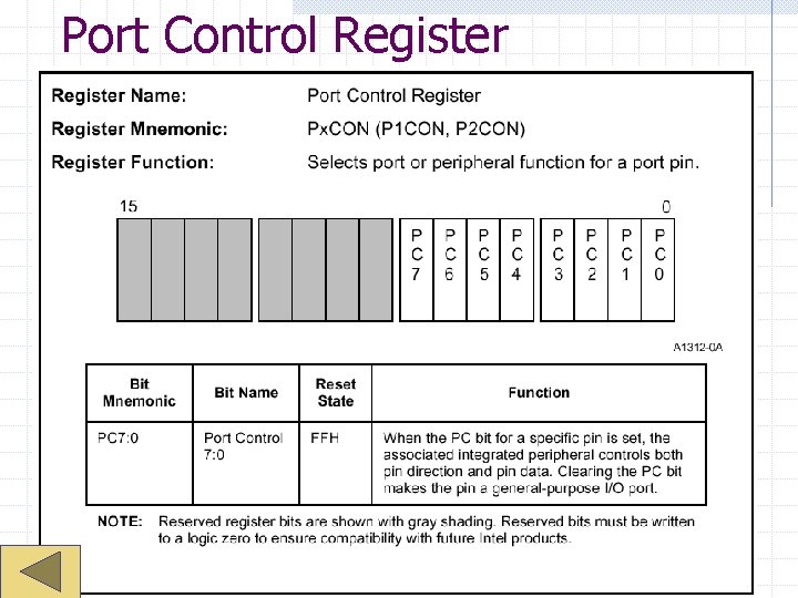
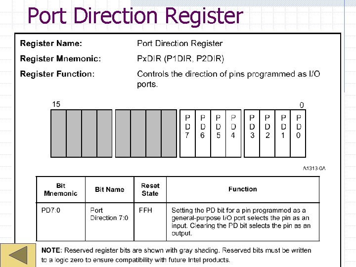
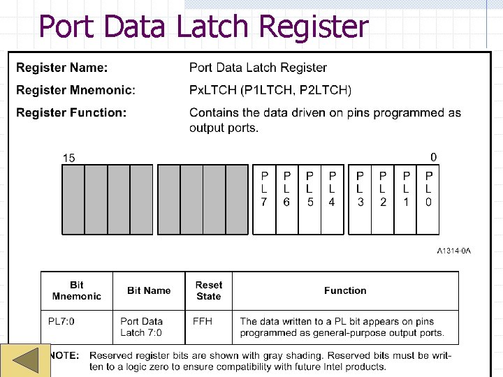
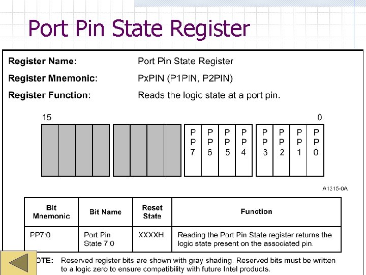
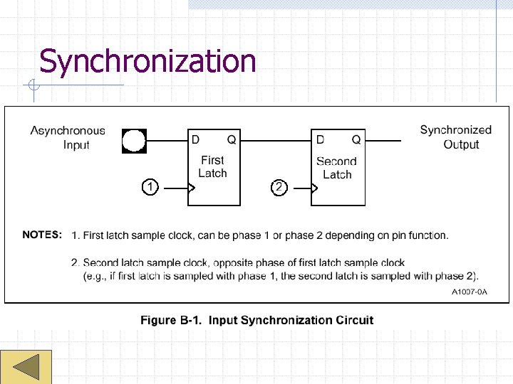
80 C 188 EB Integrated I/O Unit Port 1 Functions Port 2 Functions Bidirectional pin structure n Synchronizer Programming n n Port Control Register Direction Register Data Latch Register Pin State Register

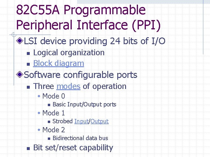
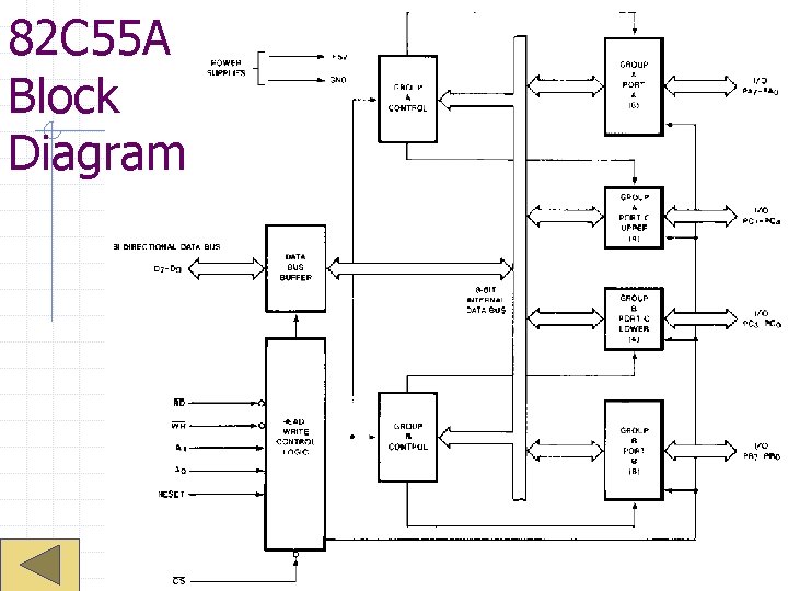
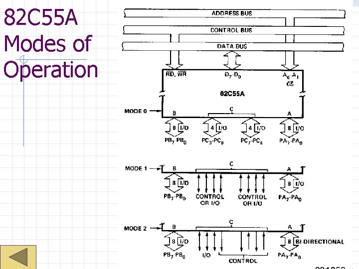
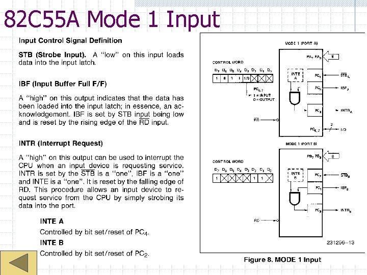
82 C 55 A Programmable Peripheral Interface (PPI) LSI device providing 24 bits of I/O n n Logical organization Block diagram Software configurable ports n Three modes of operation w Mode 0 n Basic Input/Output ports w Mode 1 n Strobed Input/Output w Mode 2 n n Bidirectional data bus Bit set/reset capability

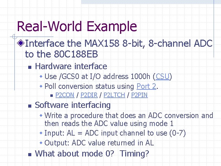
Real-World Example Interface the MAX 158 8 -bit, 8 -channel ADC to the 80 C 188 EB n Hardware interface w Use /GCS 0 at I/O address 1000 h (CSU) w Poll conversion status using Port 2. n n P 2 CON / P 2 DIR / P 2 LTCH / P 2 PIN Software interfacing w Write a procedure that does an ADC conversion and then reads the ADC value using mode 1 w Input: AL = ADC input channel to use (0 -7) w Output: ADC value returned in AL n What about mode 0? Timing?

Wrapping Up Homework #5 due Friday, 11/9/2001

Byte Input Port Example

Byte Output Port Example

74 HC 540/541

74 HC 573

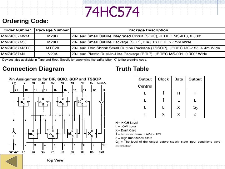
74 HC 574

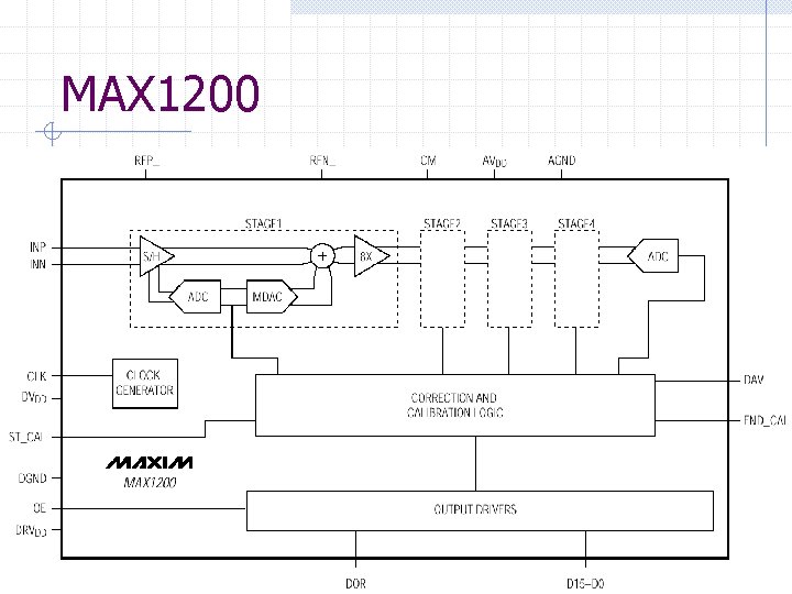
MAX 1200

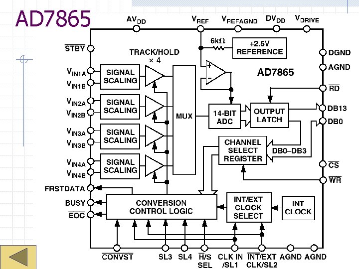
AD 7865

Generic Device Controller (Fig 12. 3 -2)

Hitachi HD 44780 U LCD Controller

Port 1 Functions

Port 2 Functions

Bidirectional Port Pin

Port Control Register

Port Direction Register

Port Data Latch Register

Port Pin State Register

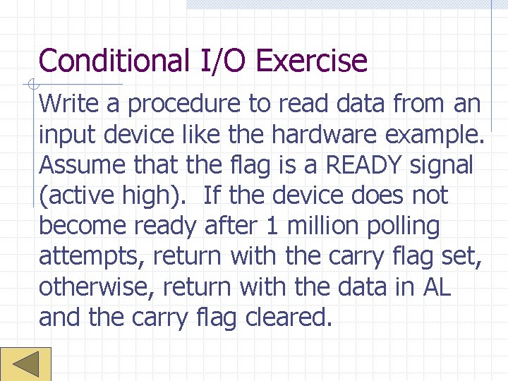
Conditional I/O Exercise Write a procedure to read data from an input device like the hardware example. Assume that the flag is a READY signal (active high). If the device does not become ready after 1 million polling attempts, return with the carry flag set, otherwise, return with the data in AL and the carry flag cleared.

82 C 55 A Block Diagram

82 C 55 A Modes of Operation

82 C 55 A Mode 1 Input

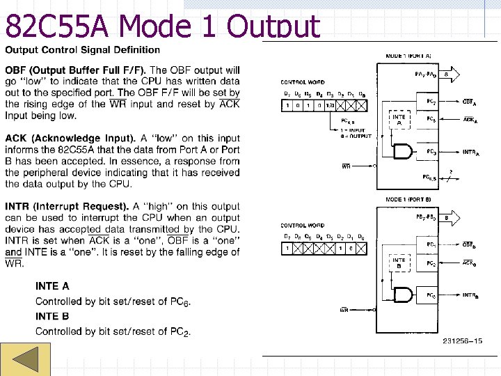
82 C 55 A Mode 1 Output

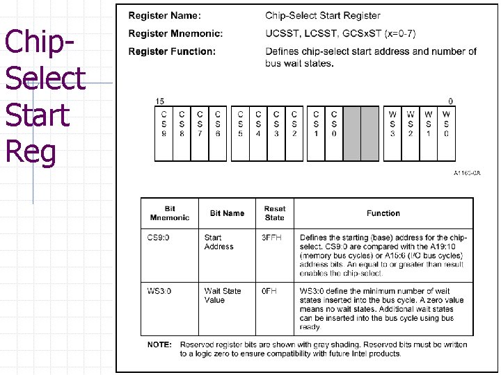
Chip. Select Start Reg

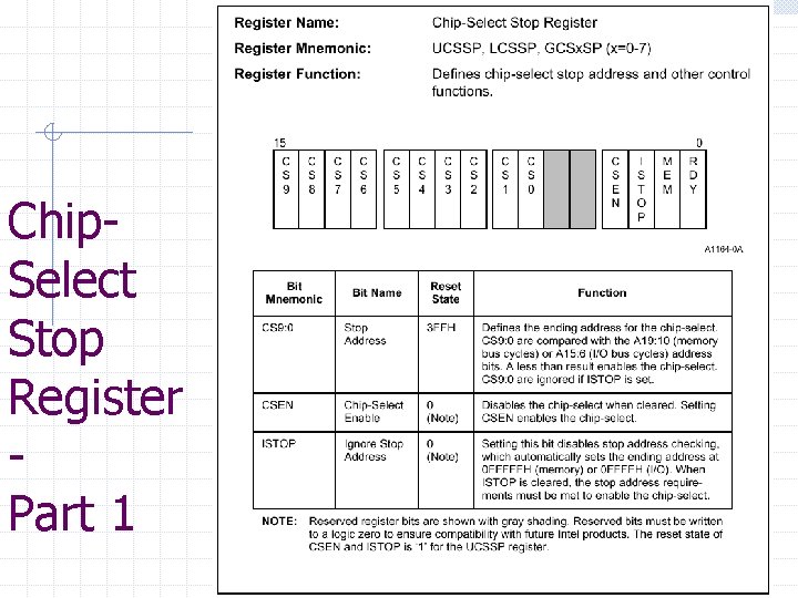
Chip. Select Stop Register Part 1

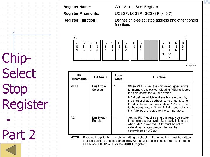
Chip. Select Stop Register Part 2

Conditional I/O Example

Synchronization