Development of Superconducting Tunnel JunctionSTJ Photon Detector on
![1. SOIFET can be operated below 800 m. K ? -Ids [A] gm [S] 1. SOIFET can be operated below 800 m. K ? -Ids [A] gm [S]](https://slidetodoc.com/presentation_image_h2/f586c14f96b27b91597119c1f084fc9a/image-10.jpg)

- Slides: 22

Development of Superconducting Tunnel Junction(STJ) Photon Detector on SOI Preamplifier Board to Search for Radiative Decays of Cosmic Neutrino Background International Conference on Technology and Instrumentation in Particle Physics ‘ 14 2 nd-6 th June 2014 in Amsterdam, the Netherlands. University of Tsukuba. A, KEKB, JAXAC, RIKEND, Okayama University. E, University of Fukui. F, Kindai University. G, Fermilab. H ◯Kota KASAHARAA, S. H. KIMA, Y. TAKEUCHIA, R. SENZAKIA, K. NAGATAA, T. OKUDAIRAA, M. KANAMARUA, T. ICHIMURAA, K. MORIUCHIA, K. KIUCHIA, Y. ARAIB, M. HAZUMIB, T. WADAC, S. MATSUURAC, S. MIMAD, H. ISHINOE, Y. KATOF, T. YOSHIDAG, E. RAMBERGH, M. KOZLOVSKYH, P. RUVINOVH, D. SEGRATSKOVH June. 6 th 2014 TIPP ‘ 14 1

Outline p. Motivation(Search for Neutrino Radiative Decay) p. Introduction of Superconducting Tunnel Junction(STJ) p. STJ on Silicon-on-Insulator Preamplifier-board(SOI-STJ) p. Current Status on Development of SOI-STJ p. Future Plan p. Summary June. 6 th 2014 TIPP ‘ 14 2

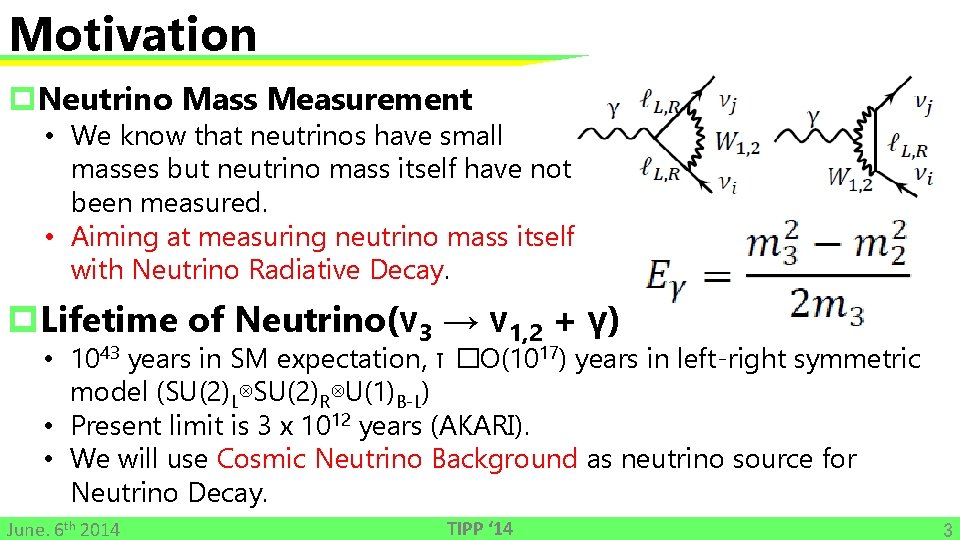
Motivation p. Neutrino Mass Measurement • We know that neutrinos have small masses but neutrino mass itself have not been measured. • Aiming at measuring neutrino mass itself with Neutrino Radiative Decay. p. Lifetime of Neutrino(ν 3 → ν 1, 2 + γ) • 1043 years in SM expectation, τ �O(1017) years in left-right symmetric model (SU(2)L⊗SU(2)R⊗U(1)B-L) • Present limit is 3 x 10¹² years (AKARI). • We will use Cosmic Neutrino Background as neutrino source for Neutrino Decay. June. 6 th 2014 TIPP ‘ 14 3

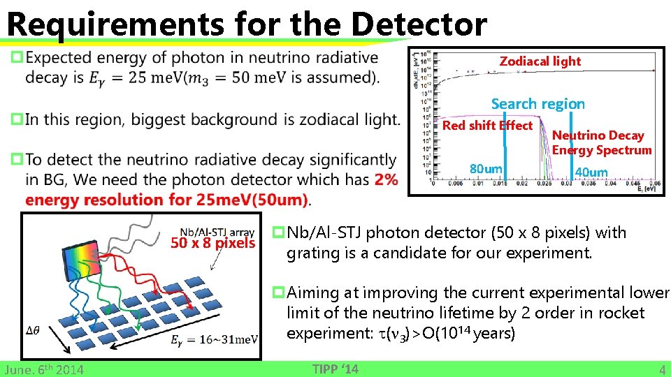
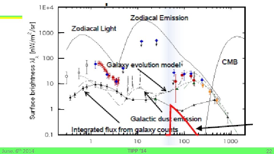
Requirements for the Detector Zodiacal light Search region Red shift Effect 80 um 50 x 8 pixels Neutrino Decay Energy Spectrum 40 um p. Nb/Al-STJ photon detector (50 x 8 pixels) with grating is a candidate for our experiment. p. Aiming at improving the current experimental lower limit of the neutrino lifetime by 2 order in rocket experiment: ( 3)>O(1014 years) June. 6 th 2014 TIPP ‘ 14 4

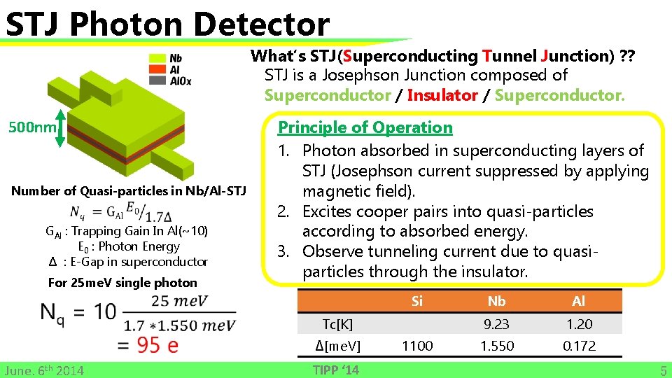
STJ Photon Detector What’s STJ(Superconducting Tunnel Junction) ? ? STJ is a Josephson Junction composed of Superconductor / Insulator / Superconductor. 500 nm Number of Quasi-particles in Nb/Al-STJ GAl : Trapping Gain In Al(~10) E 0 : Photon Energy Δ : E-Gap in superconductor For 25 me. V single photon Principle of Operation 1. Photon absorbed in superconducting layers of STJ (Josephson current suppressed by applying magnetic field). 2. Excites cooper pairs into quasi-particles according to absorbed energy. 3. Observe tunneling current due to quasiparticles through the insulator. Si Tc[K] Δ[me. V] June. 6 th 2014 TIPP ‘ 14 1100 Nb Al 9. 23 1. 20 1. 550 0. 172 5

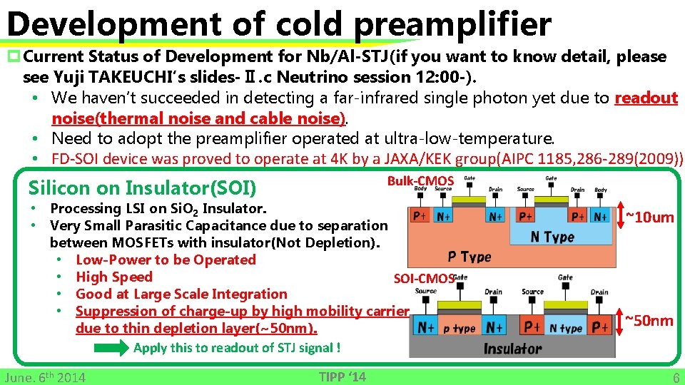
Development of cold preamplifier p. Current Status of Development for Nb/Al-STJ(if you want to know detail, please see Yuji TAKEUCHI’s slides-Ⅱ. c Neutrino session 12: 00 -). • We haven’t succeeded in detecting a far-infrared single photon yet due to readout noise(thermal noise and cable noise). • Need to adopt the preamplifier operated at ultra-low-temperature. • FD-SOI device was proved to operate at 4 K by a JAXA/KEK group(AIPC 1185, 286 -289(2009)). Bulk-CMOS Silicon on Insulator(SOI) • Processing LSI on Si. O 2 Insulator. • Very Small Parasitic Capacitance due to separation between MOSFETs with insulator(Not Depletion). • Low-Power to be Operated • High Speed SOI-CMOS • Good at Large Scale Integration • Suppression of charge-up by high mobility carrier due to thin depletion layer(~50 nm). Apply this to readout of STJ signal ! June. 6 th 2014 TIPP ‘ 14 ~10 um ~50 nm 6

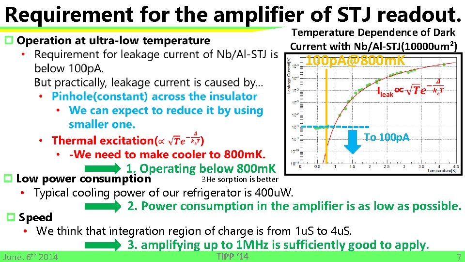
Requirement for the amplifier of STJ readout. Temperature Dependence of Dark Current with Nb/Al-STJ(10000 um 2) 100 p. A@800 m. K To 100 p. A 1. Operating below 800 m. K 3 He sorption is better p Low power consumption • Typical cooling power of our refrigerator is 400 u. W. 2. Power consumption in the amplifier is as low as possible. p Speed • We think that integration region of charge is from 1 u. S to 4 u. S. June. 6 th 2014 3. amplifying up to 1 MHz is sufficiently good to apply. TIPP ‘ 14 7

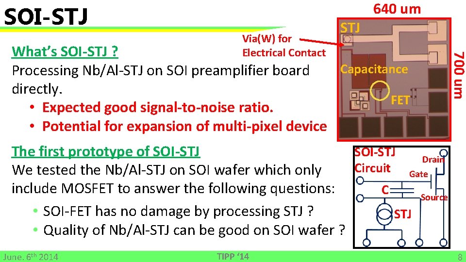
SOI-STJ What’s SOI-STJ ? Capacitance Processing Nb/Al-STJ on SOI preamplifier board directly. FET • Expected good signal-to-noise ratio. • Potential for expansion of multi-pixel device 700 um Via(W) for Electrical Contact STJ 640 um SOI-STJ The first prototype of SOI-STJ Drain Circuit Gate We tested the Nb/Al-STJ on SOI wafer which only include MOSFET to answer the following questions: C Source • SOI-FET has no damage by processing STJ ? STJ • Quality of Nb/Al-STJ can be good on SOI wafer ? June. 6 th 2014 TIPP ‘ 14 8

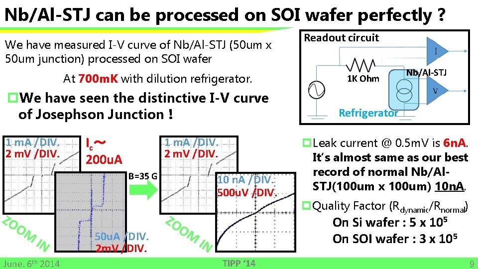
Nb/Al-STJ can be processed on SOI wafer perfectly ? We have measured I-V curve of Nb/Al-STJ (50 um x 50 um junction) processed on SOI wafer At 700 m. K with dilution refrigerator. p. We have seen the distinctive I-V curve of Josephson Junction ! 1 m. A /DIV. 2 m. V /DIV. I c~ 200 u. A 1 m. A /DIV. 2 m. V /DIV. B=35 G ZO OM IN June. 6 th 2014 50 u. A /DIV. 2 m. V /DIV. 10 n. A /DIV. 500 u. V /DIV. ZO OM Readout circuit 1 K Ohm Nb/Al-STJ Refrigerator p. Leak current @ 0. 5 m. V is 6 n. A. It’s almost same as our best record of normal Nb/Al. STJ(100 um x 100 um) 10 n. A. p. Quality Factor (Rdynamic/Rnormal) On Si wafer : 5 x 10⁵ On SOI wafer : 3 x 10⁵ IN TIPP ‘ 14 9
![1 SOIFET can be operated below 800 m K Ids A gm S 1. SOIFET can be operated below 800 m. K ? -Ids [A] gm [S]](https://slidetodoc.com/presentation_image_h2/f586c14f96b27b91597119c1f084fc9a/image-10.jpg)
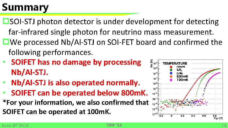
1. SOIFET can be operated below 800 m. K ? -Ids [A] gm [S] NMOS(690 -750 m. K) Ids [A] Width = 1000 um Length = 1 um I-V curve of SOIFETs after processing Nb/Al-STJ. • Both of NMOS and PMOS could be operated below 800 m. K. • Trans-conductance “gm” was not varied drastically for each temperature at operation voltage(0. 2 V). We can use these as Preamplifier for STJ signal at ultra-low temperature. PMOS(750 m. K) Vgs[V] Width = 1000 um Length = 1 um Vgs[V] PMOS gm [S] NMOS June. 6 th 2014 Vds[V] TIPP ‘ 14 Excellent performance !! 10

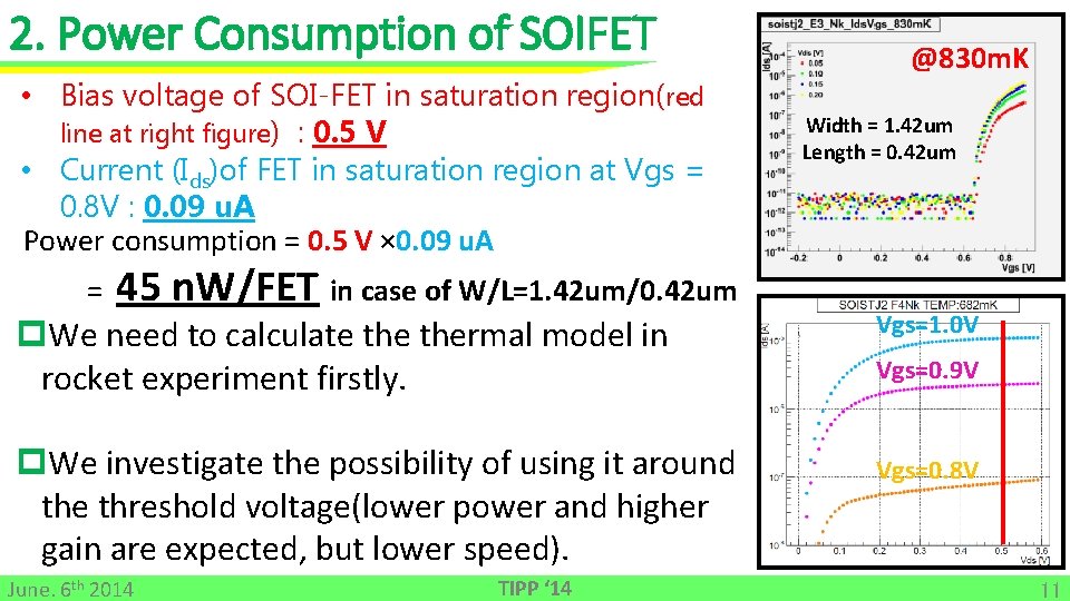
2. Power Consumption of SOIFET • Bias voltage of SOI-FET in saturation region(red line at right figure) : 0. 5 V • Current (Ids)of FET in saturation region at Vgs = 0. 8 V : 0. 09 u. A Power consumption = 0. 5 V × 0. 09 u. A = 45 n. W/FET in case of W/L=1. 42 um/0. 42 um @830 m. K Width = 1. 42 um Length = 0. 42 um p. We need to calculate thermal model in rocket experiment firstly. Vgs=1. 0 V p. We investigate the possibility of using it around the threshold voltage(lower power and higher gain are expected, but lower speed). Vgs=0. 8 V June. 6 th 2014 TIPP ‘ 14 Vgs=0. 9 V 11

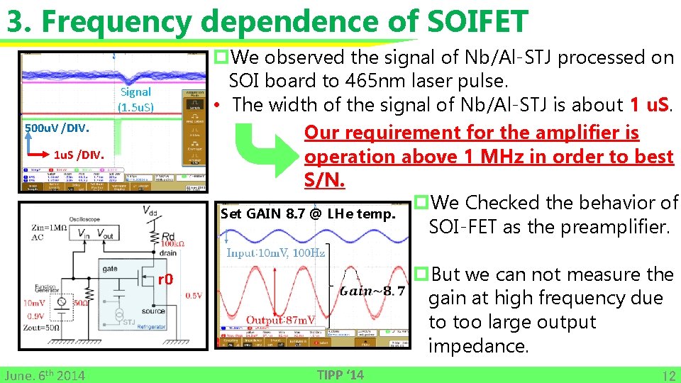
3. Frequency dependence of SOIFET p. We observed the signal of Nb/Al-STJ processed on SOI board to 465 nm laser pulse. • The width of the signal of Nb/Al-STJ is about 1 u. S. Our requirement for the amplifier is operation above 1 MHz in order to best S/N. p We Checked the behavior of Set GAIN 8. 7 @ LHe temp. SOI-FET as the preamplifier. Signal (1. 5 u. S) 500 u. V /DIV. 1 u. S /DIV. p. But we can not measure the gain at high frequency due to too large output impedance. r 0 June. 6 th 2014 TIPP ‘ 14 12

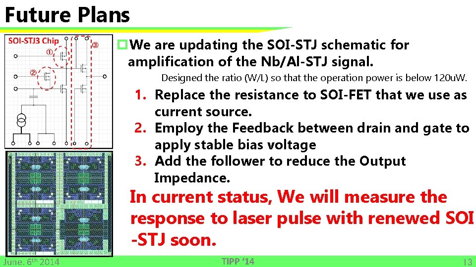
Future Plans p. We are updating the SOI-STJ schematic for amplification of the Nb/Al-STJ signal. Designed the ratio (W/L) so that the operation power is below 120 u. W. 1. Replace the resistance to SOI-FET that we use as current source. 2. Employ the Feedback between drain and gate to apply stable bias voltage 3. Add the follower to reduce the Output Impedance. In current status, We will measure the response to laser pulse with renewed SOI -STJ soon. June. 6 th 2014 TIPP ‘ 14 13

Summary p. SOI-STJ photon detector is under development for detecting far-infrared single photon for neutrino mass measurement. p. We processed Nb/Al-STJ on SOI-FET board and confirmed the following performances. • SOIFET has no damage by processing Nb/Al-STJ. • Nb/Al-STJ is also operated normally. • SOIFET can be operated below 800 m. K. *For your information, we also confirmed that SOIFET can be operated at 100 m. K. June. 6 th 2014 TIPP ‘ 14 14

Back Up Slides June. 6 th 2014 TIPP ‘ 14 15

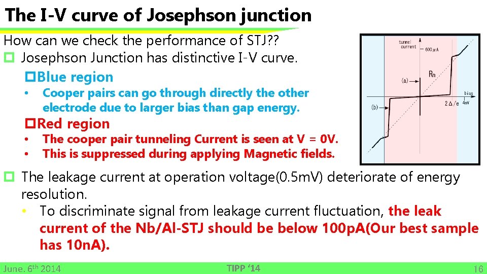
The I-V curve of Josephson junction How can we check the performance of STJ? ? p Josephson Junction has distinctive I-V curve. p. Blue region • Cooper pairs can go through directly the other electrode due to larger bias than gap energy. p. Red region • • The cooper pair tunneling Current is seen at V = 0 V. This is suppressed during applying Magnetic fields. p The leakage current at operation voltage(0. 5 m. V) deteriorate of energy resolution. • To discriminate signal from leakage current fluctuation, the leak current of the Nb/Al-STJ should be below 100 p. A(Our best sample has 10 n. A). June. 6 th 2014 TIPP ‘ 14 16

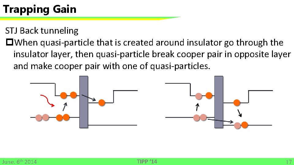
Trapping Gain STJ Back tunneling p. When quasi-particle that is created around insulator go through the insulator layer, then quasi-particle break cooper pair in opposite layer and make cooper pair with one of quasi-particles. June. 6 th 2014 TIPP ‘ 14 17

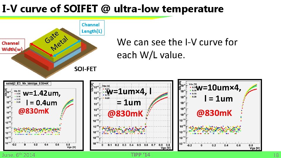
I-V curve of SOIFET @ ultra-low temperature Channel Width(w) te l a G eta M Channel Length(L) We can see the I-V curve for each W/L value. SOI-FET w=1. 42 um, l = 0. 4 um @830 m. K June. 6 th 2014 w=1 um× 4, l = 1 um @830 m. K TIPP ‘ 14 w=10 um× 4, l = 1 um @830 m. K 18

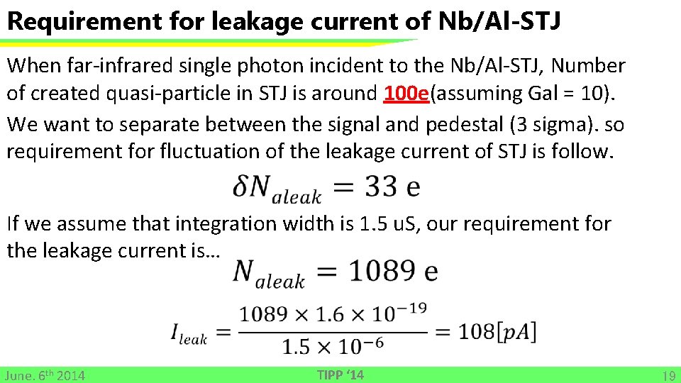
Requirement for leakage current of Nb/Al-STJ When far-infrared single photon incident to the Nb/Al-STJ, Number of created quasi-particle in STJ is around 100 e(assuming Gal = 10). We want to separate between the signal and pedestal (3 sigma). so requirement for fluctuation of the leakage current of STJ is follow. If we assume that integration width is 1. 5 u. S, our requirement for the leakage current is… June. 6 th 2014 TIPP ‘ 14 19

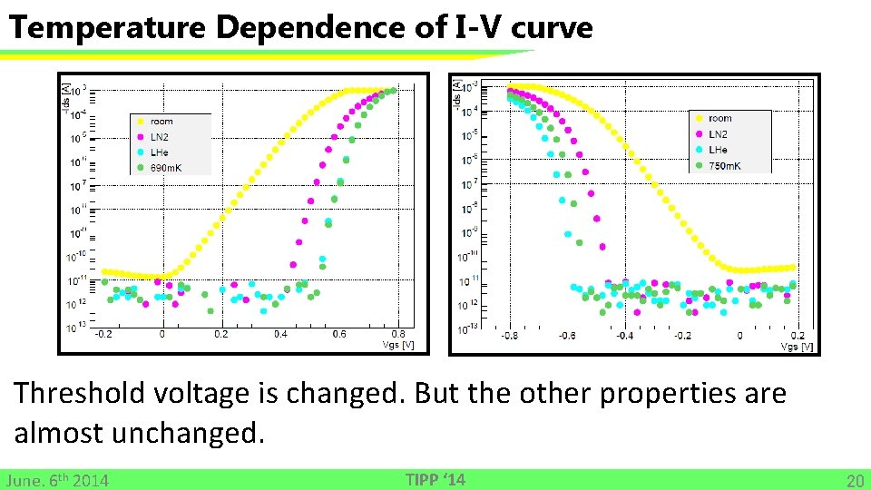
Temperature Dependence of I-V curve Threshold voltage is changed. But the other properties are almost unchanged. June. 6 th 2014 TIPP ‘ 14 20

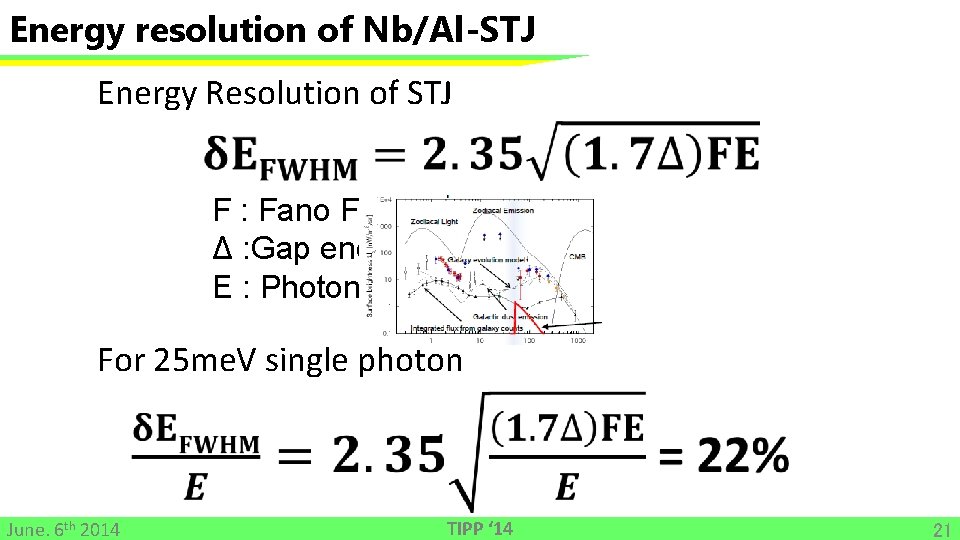
Energy resolution of Nb/Al-STJ Energy Resolution of STJ F : Fano Factor Δ : Gap energy E : Photon energy For 25 me. V single photon June. 6 th 2014 TIPP ‘ 14 21

June. 6 th 2014 TIPP ‘ 14 22