ConfigurationProgram Method for Altera Device 1999 Altera Corporation


- Slides: 19

Configuration/Program Method for Altera Device © 1999 Altera Corporation

Configure FLEX device by Micro-processor 8031 (use the TTF file) © 1999 Altera Corporation

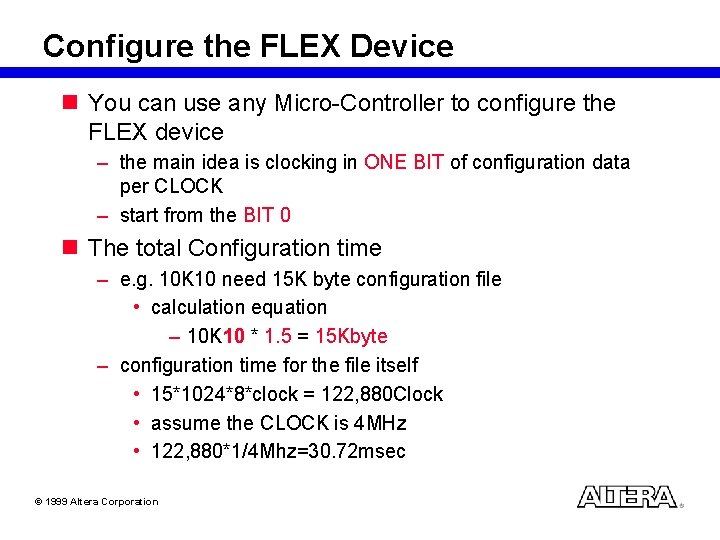
Configure the FLEX Device n You can use any Micro-Controller to configure the FLEX device – the main idea is clocking in ONE BIT of configuration data per CLOCK – start from the BIT 0 n The total Configuration time – e. g. 10 K 10 need 15 K byte configuration file • calculation equation – 10 K 10 * 1. 5 = 15 Kbyte – configuration time for the file itself • 15*1024*8*clock = 122, 880 Clock • assume the CLOCK is 4 MHz • 122, 880*1/4 Mhz=30. 72 msec © 1999 Altera Corporation

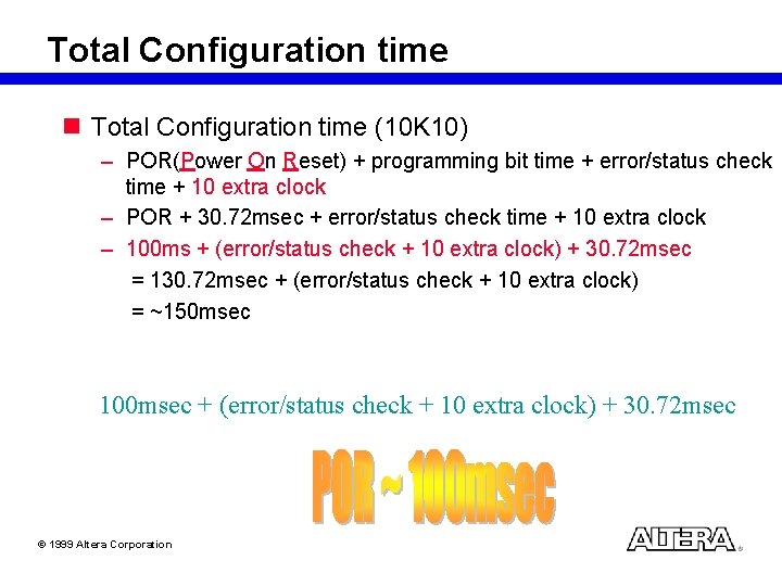
Total Configuration time n Total Configuration time (10 K 10) – POR(Power On Reset) + programming bit time + error/status check time + 10 extra clock – POR + 30. 72 msec + error/status check time + 10 extra clock – 100 ms + (error/status check + 10 extra clock) + 30. 72 msec = 130. 72 msec + (error/status check + 10 extra clock) = ~150 msec 100 msec + (error/status check + 10 extra clock) + 30. 72 msec © 1999 Altera Corporation

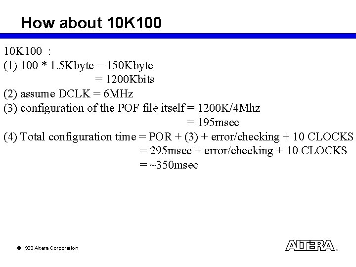
How about 10 K 100 : (1) 100 * 1. 5 Kbyte = 150 Kbyte = 1200 Kbits (2) assume DCLK = 6 MHz (3) configuration of the POF file itself = 1200 K/4 Mhz = 195 msec (4) Total configuration time = POR + (3) + error/checking + 10 CLOCKS = 295 msec + error/checking + 10 CLOCKS = ~350 msec © 1999 Altera Corporation

PS (Passive Serial) Pin Information © 1999 Altera Corporation

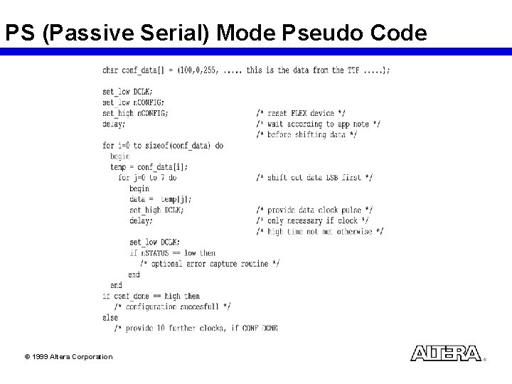
PS (Passive Serial) Mode Pseudo Code © 1999 Altera Corporation

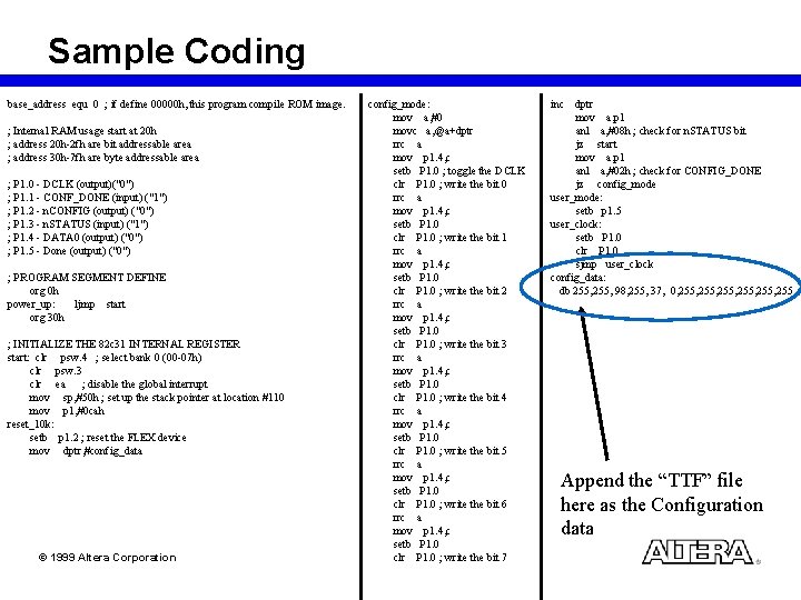
Sample Coding base_address equ 0 ; if define 00000 h, this program compile ROM image. ; Internal RAM usage start at 20 h ; address 20 h-2 fh are bit addressable area ; address 30 h-7 fh are byte addressable area ; P 1. 0 - DCLK (output)("0") ; P 1. 1 - CONF_DONE (input) ("1") ; P 1. 2 - n. CONFIG (output) ("0") ; P 1. 3 - n. STATUS (input) ("1") ; P 1. 4 - DATA 0 (output) ("0") ; P 1. 5 - Done (output) ("0") ; PROGRAM SEGMENT DEFINE org 0 h power_up: ljmp start org 30 h ; INITIALIZE THE 82 c 31 INTERNAL REGISTER start: clr psw. 4 ; select bank 0 (00 -07 h) clr psw. 3 clr ea ; disable the global interrupt mov sp, #50 h ; set up the stack pointer at location #110 mov p 1, #0 cah reset_10 k: setb p 1. 2 ; reset the FLEX device mov dptr, #config_data © 1999 Altera Corporation config_mode: mov a, #0 movc a, @a+dptr rrc a mov p 1. 4, c setb P 1. 0 ; toggle the DCLK clr P 1. 0 ; write the bit 0 rrc a mov p 1. 4, c setb P 1. 0 clr P 1. 0 ; write the bit 1 rrc a mov p 1. 4, c setb P 1. 0 clr P 1. 0 ; write the bit 2 rrc a mov p 1. 4, c setb P 1. 0 clr P 1. 0 ; write the bit 3 rrc a mov p 1. 4, c setb P 1. 0 clr P 1. 0 ; write the bit 4 rrc a mov p 1. 4, c setb P 1. 0 clr P 1. 0 ; write the bit 5 rrc a mov p 1. 4, c setb P 1. 0 clr P 1. 0 ; write the bit 6 rrc a mov p 1. 4, c setb P 1. 0 clr P 1. 0 ; write the bit 7 inc dptr mov a, p 1 anl a, #08 h ; check for n. STATUS bit jz start mov a, p 1 anl a, #02 h ; check for CONFIG_DONE jz config_mode user_mode: setb p 1. 5 user_clock: setb P 1. 0 clr P 1. 0 sjmp user_clock config_data: db 255, 98, 255, 37, 0, 255, 255 Append the “TTF” file here as the Configuration data

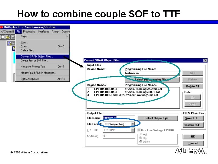
How to combine couple SOF to TTF © 1999 Altera Corporation

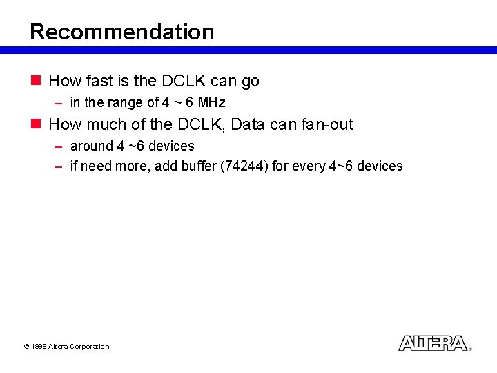
Recommendation n How fast is the DCLK can go – in the range of 4 ~ 6 MHz n How much of the DCLK, Data can fan-out – around 4 ~6 devices – if need more, add buffer (74244) for every 4~6 devices © 1999 Altera Corporation

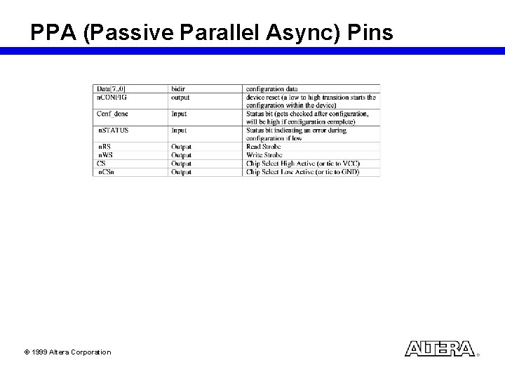
PPA (Passive Parallel Async) Pins © 1999 Altera Corporation

PPA Mode Pseudo Code © 1999 Altera Corporation

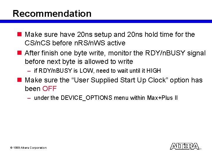
Recommendation n Make sure have 20 ns setup and 20 ns hold time for the CS/n. CS before n. RS/n. WS active n After finish one byte write, monitor the RDY/n. BUSY signal before next byte is allowed to write – if RDY/n. BUSY is LOW, need to wait until it HIGH n Make sure the “User Supplied Start Up Clock” option has been OFF – under the DEVICE_OPTIONS menu within Max+Plus II © 1999 Altera Corporation

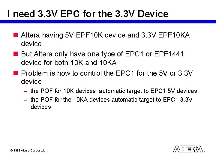
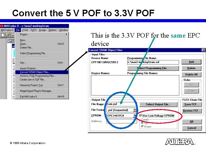
I need 3. 3 V EPC for the 3. 3 V Device n Altera having 5 V EPF 10 K device and 3. 3 V EPF 10 KA device n But Altera only have one type of EPC 1 or EPF 1441 device for both 10 K and 10 KA n Problem is how to control the EPC 1 for the 5 V or 3. 3 V device – the POF for 10 K devices automatic target to EPC 1 5 V devices – the POF for the 10 KA devices automatic target to EPC 1 3. 3 V devices © 1999 Altera Corporation

Convert the 5 V POF to 3. 3 V POF This is the 3. 3 V POF for the same EPC device © 1999 Altera Corporation

Conclusion n You can use your system micro-processor to configure any Altera FLEX device – 8 K/10 K/6 K • You can save the Serial EPROM • DCLK should be in the range of 4~6 Mhz – Don’t forget that you also need to have pull up resistors on n. STATUS, CONF_DONE pins n JTAG Port – JTAG Chain for MAX and FLEX devices • also support NON-ALTERA JTAG devices – JAM for Single/Multiple MAX devices only • also support NON-ALTERA JTAG devices © 1999 Altera Corporation

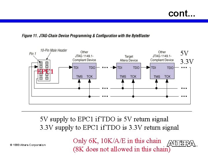
Cont. . . n PS Port – FLEX Chain for FLEX devices only – can not mix the FLEX devices n FLEX A/E devices I/O accept 5 V, 3. 3 V or 2. 5 V input signal (Multi-Voltage I/O) n EPC 1 is not Multi-Voltage I/O – 5 V power supply accept 5 V signal input – 3 V power supply accept 3. 3 V signal input © 1999 Altera Corporation

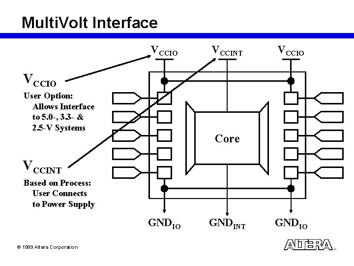
Multi. Volt Interface VCCIO VCCINT VCCIO User Option: Allows Interface to 5. 0 -, 3. 3 - & 2. 5 -V Systems Core VCCINT Based on Process: User Connects to Power Supply GNDIO © 1999 Altera Corporation GNDINT GNDIO

cont. . . 5 V 3. 3 V EPC 1 5 V supply to EPC 1 if TDO is 5 V return signal 3. 3 V supply to EPC 1 if TDO is 3. 3 V return signal © 1999 Altera Corporation Only 6 K, 10 K/A/E in this chain (8 K does not allowed in this chain)