CHAPTER6 INTRODUCTION TO IC AND SMD 6 1


 Classification on the basis of fabrication technology: 1. Monolithic")


 preparation 1. Crystal growth &doping 2. Ingot trimming & grinding 3.")


 • This type of package is made of plastic or")


 Device type")

 is a method for producing")


 Insulation Resistance film Ceramic chip Chip ( Thick Film")


 • Plastic Leaded Chip Carrier (PLCC) •")
")
 Leaded Ceramic Chip Carrier (LDCC)")


- Slides: 49
CHAPTER-6 INTRODUCTION TO IC AND SMD
6. 1 IC’S
Classification of IC’s • A) Classification on the basis of fabrication technology: 1. Monolithic ICs 2. Thin film IC 3. Thick film IC 4. Hybrid Ics • B) Classification on the basis of level of Integration: 1. Small scale integration- SSI(less than 10 gates) 2. Medium scale integration-LSI(between 11 and 99 gates) 3. Large scale integration-LSI(between 100 and 9999 gates) 4. Very large scale integration-VLSI(10000 and 99999 gates) 5. Ultra large scale integration-ULSI(more than 100000) • C) Classification on the basis of function or operation: 1. Linear ICs 2. Digital ICs
Advantages and Disadvantages of ICs • Advantages: 1. There is saving in space & weight. 2. Production time decreases as many components are fabricated on a single chip. 3. There is increase in reliability as there is used instead of discrete components. 4. Cost of equipment is decreased as IC is used of discrete components. 5. It can work satisfactory up to certain temperature. 6. lay out of the circuit becomes simple. 7. Power required for the operation of the equipment decreases.
• Disadvantages: 1. The whole IC becomes useless even when its single component fails to work. 2. It is not possible to make alterations in the circuit. 3. Capacitors of more than 30 p. F value cannot be fabricated in IC. 4. Inductors cannot be fabricated in Ics. 5. At present ICs having power rating more than 10 W cannot be manufactured.
Basic processes involved in fabricating Monolithic ICs 1. 2. 3. 4. 5. 6. 7. 8. 9. Silicon wafer (substrate) preparation Epitaxial growth Oxidation Photolithography Diffusion Ion implantation Isolation technique Metallization Assembly processing & packaging
Silicon wafer (substrate) preparation 1. Crystal growth &doping 2. Ingot trimming & grinding 3. Ingot slicing 4. Wafer policing & etching 5. Wafer cleaning Typical wafer 7
Epitaxial growth 1. 2. Epitaxy means growing a single crystal silicon structure upon a original silicon substrate, so that the resulting layer is an extension of the substrate crystal structure. The basic chemical reaction in the epitaxial growth process of pure silicon is the hydrogen reduction of silicon tetrachloride. 1200 o. C Si. Cl+ 2 H <------> Si + 4 HCl 8
Oxidation 1. Si. O 2 is an extremely hard protective coating & is unaffected by almost all reagents except by hydrochloric acid. Thus it stands against any contamination. 2. By selective etching of Si. O 2, diffusion of impurities through carefully defined through windows in the Si. O 2 can be accomplished to fabricate various components. 3. The silicon wafers are stacked up in a quartz boat & then inserted into quartz furnace tube. The Si wafers are raised to a high temperature in the range of 950 to 1150 o. C & at the same time, exposed to a gas containing O 2 or H 2 O or both. The chemical action is Si + 2 HO------> Si O 2+ 2 H 2 9
Photographic mask The development of photographic mask involves the preparation of initial artwork and its diffusion. reduction, decomposition of initial artwork or layout into several mask layers. Photo etching 10
Diffusion 11
Ion implantation technique 1. It is performed at low temperature. Therefore, previously diffused regions have a lesser tendency for lateral spreading. 2. In diffusion process, temperature has to be controlled over a large area inside the oven, where as in ion implantation process, accelerating potential & beam content are dielectrically controlled from outside. 12
Dielectric isolation In dielectric isolation, a layer of solid dielectric such as Si. O 2 or ruby completely surrounds each components thereby producing isolation, both electrical & physical. This isolating dielectric layer is thick enough so that its associated capacitance is negligible. Also, it is possible to fabricate both pnp & npn transistors within the same silicon substrate. 13
Metallization The process of producing a thin metal film layer that will serve to make interconnection of the various components on the chip is called metallization. 14
Aluminum is preferred for metallization 1. 2. 3. 4. It is a good conductor it is easy to deposit aluminum films using vacuum deposition. It makes good mechanical bonds with silicon It forms a low resistance contact 15
IC packages available 1. 2. 3. Metal can package. Dual-in-line package. Ceramic flat package. 16
Thin film ICs • In this material is deposited on the insulating substrate like glass or ceramic. • For this vacuum or vapor deposit method is employed. • The thickness of the film is 50 to 20000 A°. • In this only the passive components like resistors and capacitors are fabricated. • Active components are not fabricated in this type of IC.
• This IC is fabricated by depositing films of conducting material on the surface of a glass or ceramic base. The resistors are fabricated by controlling the width and thickness of the films and by using different materials selected for their resistivity. For capacitors, a film of insulating oxide is sandwiched between two conducting films. A spiral form of film is deposited onto the IC to create an inductor. • Mainly two methods are used for producing thin films. One method, called vacuum evaporation is used in which vaporized material is deposited on a substrate contained in a vacuum. The other method is called cathode sputtering in which atoms from a cathode made of the desired film material are deposited on a substrate located between a cathode and an anode.
Thick film ICs • They are also commonly called as printed thin film circuits. The desired circuit pattern is obtained on a ceramic substance by using a manufacturing process called silk-screen printing technique. • The inks used for printing are usually materials that have resistive, conductive, or dielectric properties. They are selected accordingly by the manufacturer. The screens are actually made of fine stainless steel wire mesh. The films are fused to the substrate after printing by placing them in hot high temperature furnaces. • The fabrication techniques used for thin film passive components are adopted for thick films as well. As with thin-film circuits, active components are added as separate devices.
Thick and Thin Film Technology: • Film Ics are broadly classified as Thick film and thin film circuits. Thin films are the ones whose thickness vary from 50 to 20000 A and the thick films have thickness that vary between 125000 to 625000 A. However, the thickness of the film is not a critical tool for classifying, but the technology for fabricating the film classifies whether the film is thin or thick film. • Only passive components like resistors and capacitors can be fabricated using film technology. Conventional film circuits are made by depositing film capacitors on a non-conducting substrate like glass or ceramic and pre-fabricated active components
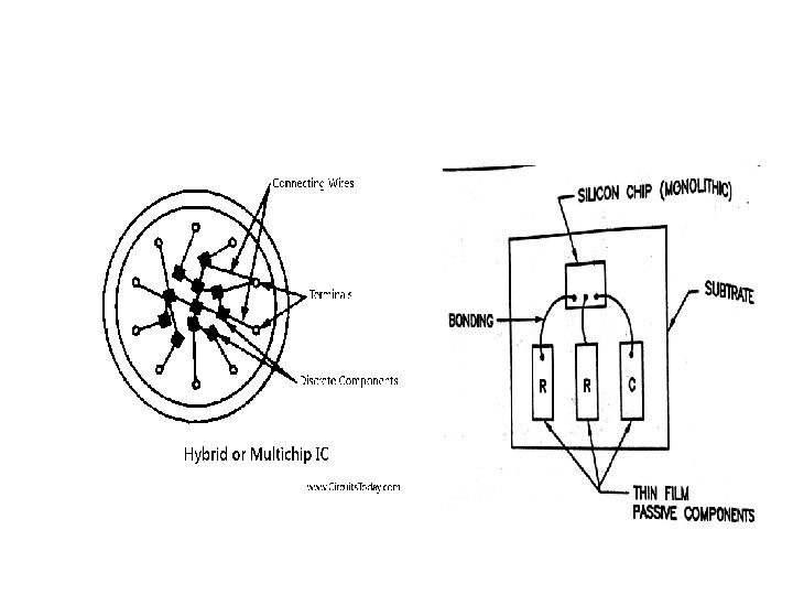
Hybrid or Multi-chip Integrated Circuits • As the name suggests, the circuit is fabricated by interconnecting a number of individual chips. Hybrids ICs are mostly used for high power audio amplifier applications from 5 Watts to more than 50 Watts. The active components are diffused transistors or diodes. The passive components may be group of diffused resistors or capacitors on a single chip, or they may be thin-film components. Interconnection between the individual chips is made by wiring process or a metalized pattern.
• The diagram of a hybrid or multi-chip IC is shown in the figure above. Hybrid IC’s are also known to provide a better performance than monolithic IC’s. Although the process is too expensive for mass production, multi-chip techniques are quite economical for small quantity production and are more often used as prototypes for monolithic ICs. • Based upon the active devices employed the ICs can be classified as bipolar ICs using bipolar active devices (BJT) and unipolar IC’s using unipolar active devices like FET.
Linear IC • • Ø Ø Ø Ø This type of IC is called Analog type IC In this input and output signals are continuous. Active device is operated in its active region. Some linear ICs are listed below, Operational amplifier Small signal amplifier Power amplifier RF and IF amplifier Microwave amplifier Multiplier Voltage comparator and regulator
Digital IC • In this IC the input and output are in logic 0 and 1. • In this the active device operates in its saturation and cutoff region. • Some digital ICs are listed below, Ø Logic gates Ø Flipflop Ø Counter Ø Multiplexer/demultiplexer Ø Encoder/Decoder Ø Shift register Ø Comparator Ø Calculator chip Ø Memory chip
IC packages-SIP • SIP – Single in line packages. • This type of package is made of plastic or ceramic body. • There is only one line of the pins. • Metal strip is provided for heat sink.
TO 5 package • In this the enclosure is made of aluminum alloy or KOVAR alloy. • There are 8 or 10 or flying leads. • Magnetic shielding is available due to the metal enclosure and heat sink can be used.
Flat package • In this the package is of square or rectangular shape. • It is made of alloy of Al 2 O 3 Mg. O and Si. O 2. • Leads are made of KOVAR (alloy of Fe, Ni and Co). • This type of package occupies less space but it is difficult to remove once soldered. • It measure 10 mm* 6 mm* 1. 3 mm.
DIP(Dual in line package) • This type of package is made of plastic or ceramic. • Such type of package is used with IC. • Numbers of pins are 8, 14, 16, 20 or 40.
Pin Identification-SIP • In this a metal strip is given on the top portion. • A notch is provided on one side. • Pin near the notch becomes pin no. 1. • Then moving further, there will be pin nos. 2, 3, 4…. etc.
TO 5 • In this a small projection is given on the metal can. • IC is kept vertical on its leads. • Lead near the projection in anti clock wise direction is lead no. 1. • Then moving further in the anticlockwise direction there will be pin nos. 2, 3, 4…. etc.
Flat • In this also a dot mark is given. • Pin near the dot mark is pin no. 1. • Then by moving in the anti clock wise direction there will be pin nos. 2, 3…. etc.
DIP • In this a notch is provided on the top or a dot mark is given. • The pin at the left of the notch as shown in fig. is pin no. 1. • Then moving in the anti clock wise direction there will be pin nos. 2, 3, 4…etc.
Temperature range • Depending upon applications there are following three temperature ranges of the integrated circuits (1) For military use : -55°C to +125°C (2) Industrial use : -20°C to +85°C (3) Commercial use : 0°C to +70°C
Device identification
• Following information is given on IC for its identification. (1) Device type number: Ø This is in three parts. Ø Prefix shows, the manufacturer’ name. Ø Then in the middle device type number such as 6890 is given. Ø Suffix indicates the package type and the temperature range. (2) Manufacturer’s logo: Ø This is normally given at the top left. (3) Data code: Ø First two numbers indicate the year of manufacture and the next two numbers indicate the production batch number. Ø For example in fig. the date code is 1286, which shows that the year of manufacturing is 2012 and the batch no. is 86.
6. 2 SMD
Concept of SMT & SMD • Surface-mount technology (SMT) is a method for producing electronic circuits in which the components are mounted or placed directly onto the surface of printed circuit boards (PCBs). An electronic device so made is called a surface-mount device (SMD). • In the industry it has largely replaced the through-hole technology construction method of fitting components with wire leads into holes in the circuit board. Both technologies can be used on the same board for components not suited to surface mounting such as large transformers and heat-sinked power semiconductors. • An SMT component is usually smaller than its through-hole counterpart because it has either smaller leads or no leads at all. It may have short pins or leads of various styles, flat contacts, a matrix of solder balls (BGAs), or terminations on the body of the component.
Advantages &Disadvantages of SMD Advantages: Decrease in the size of PCB. Use of double sided Printed circuit board. Sub miniature circuit. Automatic assembly. Reduced cost. Improvement in circuit performance. Disadvantages: Design is difficult. Highly skilled workers are needed for SMT work. However most of the work is carried by computers and robots. Ø For SMD zero defect manufacturing is needed. For this accurate process control has to be done. • Ø Ø Ø • Ø Ø
SMD Resistor • There are two types of surface mount resistor on the basis of fabrication technology. (1) Thick film type (2) Thin film type • Types of SMD resistors: (1) Carbon composition (2) Ceramic composition (3) Metal film (4) Wire wound (5) Power film resistor Surface Mount Resistors
Chip ( Thin Film ) Insulation Resistance film Ceramic chip Chip ( Thick Film ) Insulation Resistance film Ceramic chip Formed Leads
SMD Capacitor • some types of surface mount type capacitors are as given below. (1) Ceramic capacitor (2) Tantalum capacitor (3) Electrolytic capacitor Surface Mount Tantalum Capacitors Surface Mount Ceramic Capacitors Multilayer Ceramic Capacitors
SMD IC • Plastic or Ceramic IC Packages? • Plastic: – Not hermetic – Low price in large quantities – High initial cost – Low thermal conductivity – Limited time at high temperature – Thermal mismatch to Si chip and metals – Not suitable for high frequency circuits • Ceramic: – Hermetic, good reliability – Costly, but OK for prototyping – Good thermal conductivity – Low thermal coefficient of expansion, matches well with Si, mismatch to organic substrates – Gold metallization must be removed – Well defined high frequency properties
SMD IC Packages • Small Outline (SO) • Plastic Leaded Chip Carrier (PLCC) • Leadless Chip Carrier (LLCC) • Leaded Ceramic Chip Carrier (LDCC) • Flatpack, mini-flatpack • Tape. Pak • Chip Scale Packages Surface mounted SO (Small Outline) IC package
SMD IC Packages: Plastic Leaded Chip Carrier (PLCC)
Leadless Chip Carrier (LLCC) Leaded Ceramic Chip Carrier (LDCC)
Flatpacks And Tape. Pak Flatpacks Tape. Pak
Diode and Transistor SOT-packages for SMD diodes and transistors: The most common, SOT-23 top left, SOT-89 for power transistors in the middle, and SOT-143 with four terminals to the right. The dimensions for SOT-23 are shown bottom left, and a cutthrough SOT-89 in the middle. Ceramic SMD transistor packages with terminal placement like for SOT-23 are shown bottom right.
Types of SMT • • Surface mount technology is divided in to three types: Type I: All SMTs top and bottom Type II: Mixed technology in both top and bottom Type III: Conventional technology on top and SMT on Bottom.