CHAPTER 4 PN JUNCTION DIODE AND RECTIFIERS 4

- Slides: 34

CHAPTER -4 PN JUNCTION DIODE AND RECTIFIERS

4. 1 PN JUNCTION DIODES

• Electronic Materials: • The goal of electronic materials is to generate and control the flow of an electrical current. • Electronic materials include: 1. Conductors: have low resistance which allows electrical current flow 2. Insulators: have high resistance which suppresses electrical current flow 3. Semiconductors: can allow or suppress electrical current flow. • Semiconductors: • Semiconductors are materials that essentially can be conditioned to act as good conductors, or good insulators, or any thing in between. • Common elements such as carbon, silicon, and germanium are semiconductors. • Silicon is the best and most widely used semiconductor.

Doping • To make the semiconductor conduct electricity, other atoms called impurities must be added. • “Impurities” are different elements. • This process is called doping.

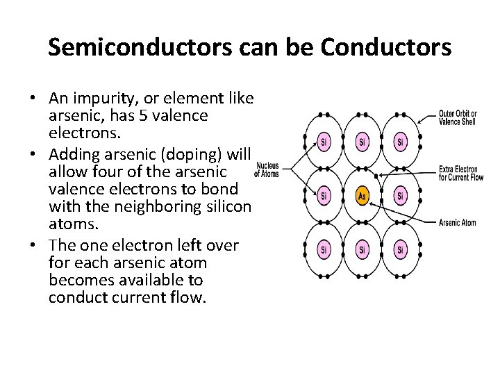
Semiconductors can be Conductors • An impurity, or element like arsenic, has 5 valence electrons. • Adding arsenic (doping) will allow four of the arsenic valence electrons to bond with the neighboring silicon atoms. • The one electron left over for each arsenic atom becomes available to conduct current flow.

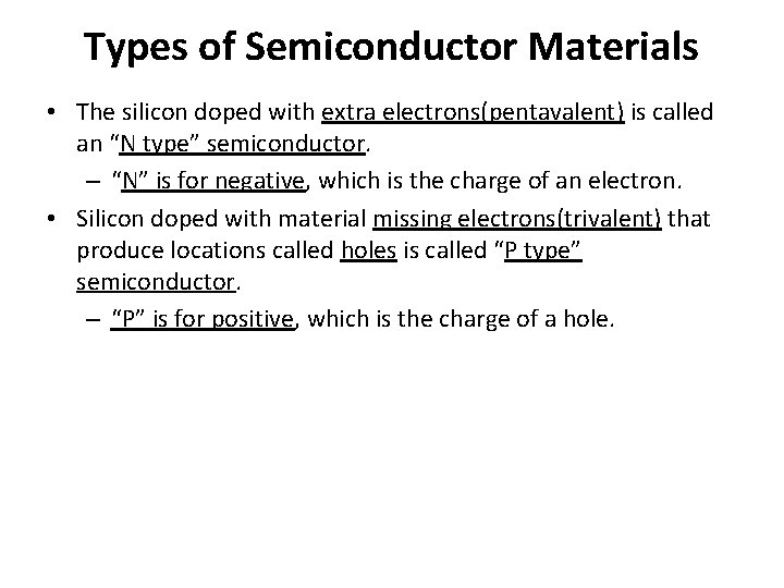
Types of Semiconductor Materials • The silicon doped with extra electrons(pentavalent) is called an “N type” semiconductor. – “N” is for negative, which is the charge of an electron. • Silicon doped with material missing electrons(trivalent) that produce locations called holes is called “P type” semiconductor. – “P” is for positive, which is the charge of a hole.

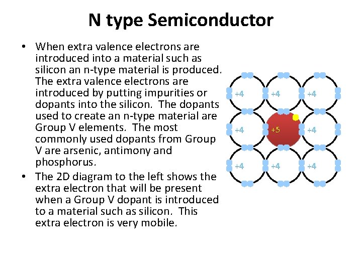
N type Semiconductor • When extra valence electrons are introduced into a material such as silicon an n-type material is produced. The extra valence electrons are introduced by putting impurities or dopants into the silicon. The dopants used to create an n-type material are Group V elements. The most commonly used dopants from Group V are arsenic, antimony and phosphorus. • The 2 D diagram to the left shows the extra electron that will be present when a Group V dopant is introduced to a material such as silicon. This extra electron is very mobile. +4 +4 +5 +4 +4

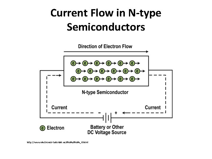
Current Flow in N-type Semiconductors http: //www. electronics-tutorials. ws/diode_6. html

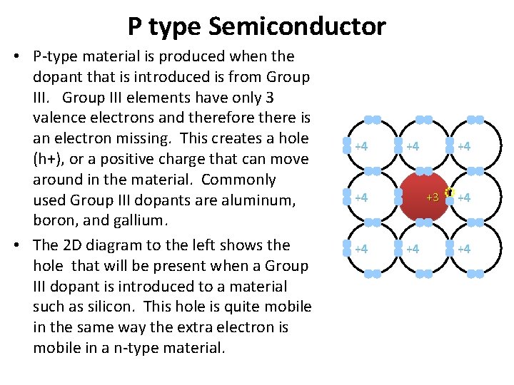
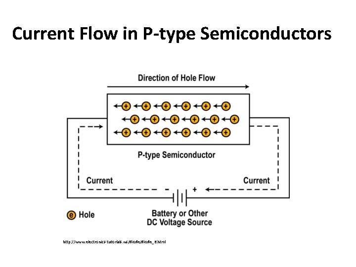
P type Semiconductor • P-type material is produced when the dopant that is introduced is from Group III elements have only 3 valence electrons and therefore there is an electron missing. This creates a hole (h+), or a positive charge that can move around in the material. Commonly used Group III dopants are aluminum, boron, and gallium. • The 2 D diagram to the left shows the hole that will be present when a Group III dopant is introduced to a material such as silicon. This hole is quite mobile in the same way the extra electron is mobile in a n-type material. +4 +4 +4 +3 +4 +4 +4

Current Flow in P-type Semiconductors http: //www. electronics-tutorials. ws/diode_6. html

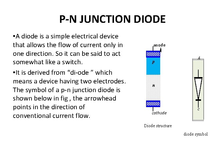
P-N JUNCTION DIODE • A diode is a simple electrical device that allows the flow of current only in one direction. So it can be said to act somewhat like a switch. • It is derived from “di-ode ” which means a device having two electrodes. The symbol of a p-n junction diode is shown below in fig , the arrowhead points in the direction of conventional current flow. anode p A n cathode c Diode structure diode symbol

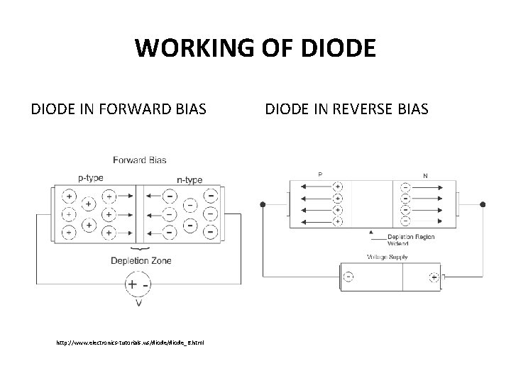
WORKING OF DIODE IN FORWARD BIAS http: //www. electronics-tutorials. ws/diode_6. html DIODE IN REVERSE BIAS

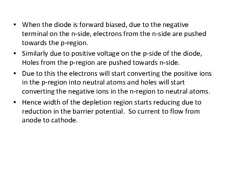
• When the diode is forward biased, due to the negative terminal on the n-side, electrons from the n-side are pushed towards the p-region. • Similarly due to positive voltage on the p-side of the diode, Holes from the p-region are pushed towards n-side. • Due to this the electrons will start converting the positive ions in the p-region into neutral atoms and holes will start converting the negative ions in the n-region to neutral atoms. • Hence width of the depletion region starts reducing due to reduction in the barrier potential. So current to flow from anode to cathode.

• When the diode is reverse biased the hole from the p-side will get attracted towards the negative terminal of the supply and electrons from the n-side are attracted towards the positive terminal. • Hence the process of widening of the depletion region takes place and hence more and more opposition to the flow of current takes place.

Characteristics of PN junction diode

• Knee voltage: The forward voltage at which the current through the forward biased diode starts to increase rapidly is known as the knee voltage. • Breakdown voltage: The reverse voltage at which the junction breaks down and results in sudden increase in reverse current is known as the breakdown voltage. • Forward voltage drop: Current flows through the diode when it is connected in the circuit and forward bias is given. Some voltage drop occurs across the diode due to the bulk resistance of diode. This voltage drop is called the forward voltage drop.

• Reverse saturation current: When diode is reverse biased current flows in reverse direction. value of this current is very small and it is almost constant. Its value does not depend on the value of the reverse voltage but it is temperature dependent. This current is called reverse saturation current. • Reverse breakdown voltage: Very small reverse current flows due to the minority charge carriers when the junction diode is reverse biased. Value of this reverse current does not depend upon the magnitude of the reverse voltage up to certain value. When the reverse voltage exceeds this value, the reverse current starts increasing rapidly. The value of the reverse voltage at which the reverse current starts increasing rapidly is known as the Reverse breakdown voltage.

4. 2 RECTIFIER

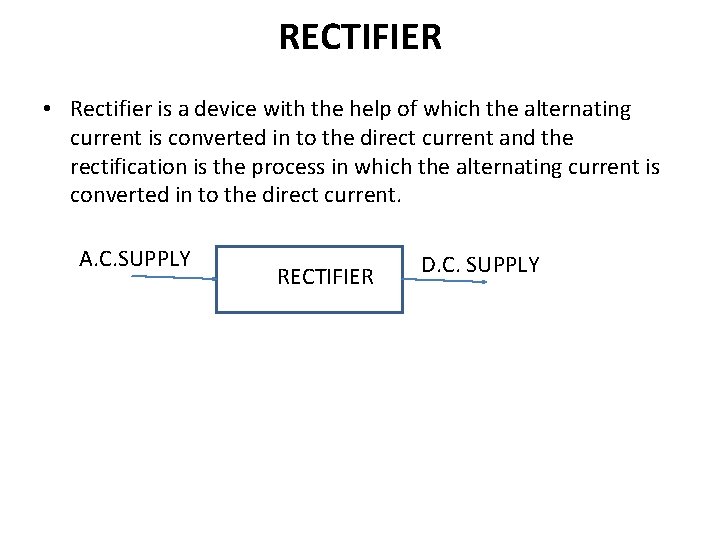
RECTIFIER • Rectifier is a device with the help of which the alternating current is converted in to the direct current and the rectification is the process in which the alternating current is converted in to the direct current. A. C. SUPPLY RECTIFIER D. C. SUPPLY

• NEED OF RECTIFIER: Almost all electronic circuits operate on d. c. supply e. g. amplifier, oscillator, radio and T. V. receiver etc. so d. c. supply is obtained from a. c. by using rectifier. Thus we operate electronic equipment on a. c. supply but inside it, the necessary d. c. supply is obtained by using rectifier. • TYPES OF RECTIFIER: 1) HALF WAVE RECTIFIER 2)FULL WAVE RECTIFIER 3) BRIDGE RECTIFIER

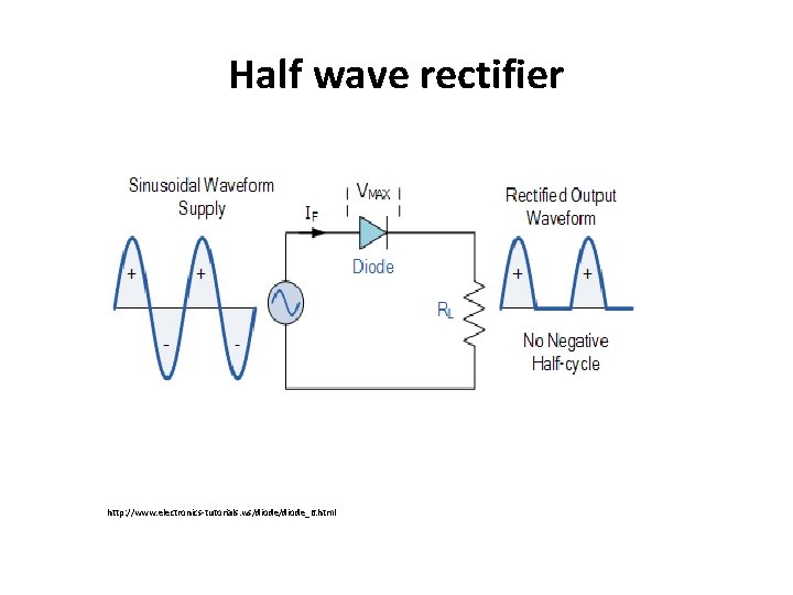
Half wave rectifier http: //www. electronics-tutorials. ws/diode_6. html

• During each “positive” half cycle of the AC sine wave, the diode is forward biased as the anode is positive with respect to the cathode resulting in current flowing through the diode. • so we get output during positive half cycle as shown in waveform. • During each “negative” half cycle of the AC sinusoidal input waveform, the diode is reverse biased as the anode is negative with respect to the cathode. Therefore, NO current flows through the diode or circuit. • So we cant get out put at resistor during negative half cycle is zero.

FULL WAVE RECTIFIER http: //www. electronics-tutorials. ws/diode_6. html

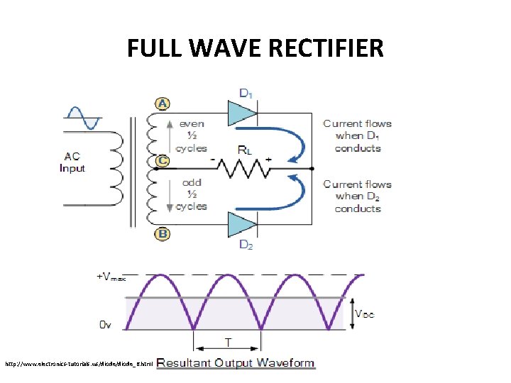
• In a Full Wave Rectifier circuit two diodes are now used, one for each half of the cycle. A multiple winding transformer is used whose secondary winding is split equally into two halves with a common centre tapped connection. • The full wave rectifier circuit consists of two power diodes connected to a single load resistance (RL) with each diode taking it in turn to supply current to the load. • When point A of the transformer is positive with respect to point C, diode D 1 conducts in the forward direction as indicated by the arrows. • When point B is positive (in the negative half of the cycle) with respect to point C, diode D 2 conducts in the forward direction and the current flowing through resistor R is in the same direction for both half-cycles.

Full Wave Bridge Rectifier http: //www. electronics-tutorials. ws/diode_6. html

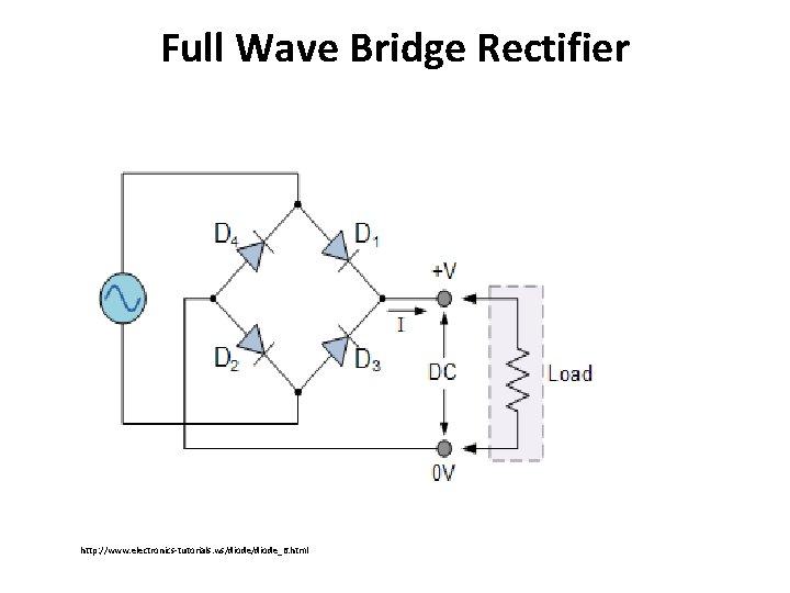
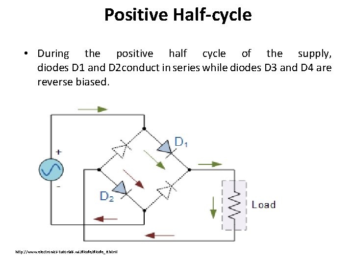
Positive Half-cycle • During the positive half cycle of the supply, diodes D 1 and D 2 conduct in series while diodes D 3 and D 4 are reverse biased. http: //www. electronics-tutorials. ws/diode_6. html

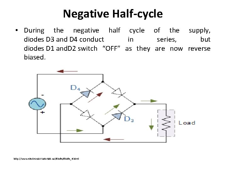
Negative Half-cycle • During the negative half cycle of the supply, diodes D 3 and D 4 conduct in series, but diodes D 1 and. D 2 switch “OFF” as they are now reverse biased. http: //www. electronics-tutorials. ws/diode_6. html

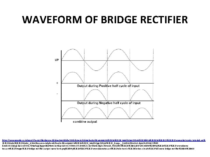
WAVEFORM OF BRIDGE RECTIFIER https: //www. google. co. in/search? q=rectifier&espv=2&biw=1440&bih=799&tbm=isch&imgil=e. Rxrl. BLwny. We. XM%253 A%253 B_Wed. Dr. Sgq. QF 8 y. M%253 Bhttp%25253 A%25252 Fwww. electronics-tutorials. ws% 25252 Fdiode%25252 Fdiode_6. html&source=iu&pf=m&fir=e. Rxrl. BLwny. We. XM%253 A%252 C_Wed. Dr. Sgq. QF 8 y. M%252 C_&usg=__5 m. DSiz. O 8 Ac 9 o. E-dq 4 s. DLJOENSSY%3 D &ved=0 CCQQyjc&ei=wl. OKVZ-f. ONahug. Shgpy 4 BQ#tbm=isch&q=WAVE+FORM+OF+BRIDGE+rectifier&imgrc=h. Owu. D_P 4 B 21 fd. M%253 A%3 Bz. Csj 9 B 76 PSn. NDM%3 Bhttp%253 A%252 Fwww. daeno tes. com%252 Fimages%252 Fbridge-rectifier-output-wave-form. png%3 Bhttp%253 A%252 Fwww. daenotes. com%252 Felectronics%252 Fdevices-circuits%252 Ffull-wave-bridge-rectifier%3 B 500%3 B 400

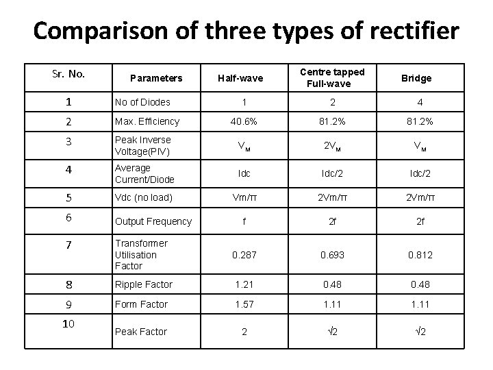
Comparison of three types of rectifier Sr. No. Parameters 1 No of Diodes 2 Max. Efficiency 3 Half-wave Centre tapped Full-wave Bridge 1 2 4 40. 6% 81. 2% Peak Inverse Voltage(PIV) VM 2 VM VM 4 Average Current/Diode Idc/2 5 Vdc (no load) Vm/π 2 Vm/π 6 Output Frequency f 2 f 2 f 7 Transformer Utilisation Factor 0. 287 0. 693 0. 812 8 Ripple Factor 1. 21 0. 48 9 Form Factor 1. 57 1. 11 Peak Factor 2 √ 2 10

Filters • The devices which converts the pulsating DC in to pure DC is called filter. • Types of filter circuit: (1) Shunt capacitor filter (2) Series inductor filter (3) Choke input LC filter (4) π filter

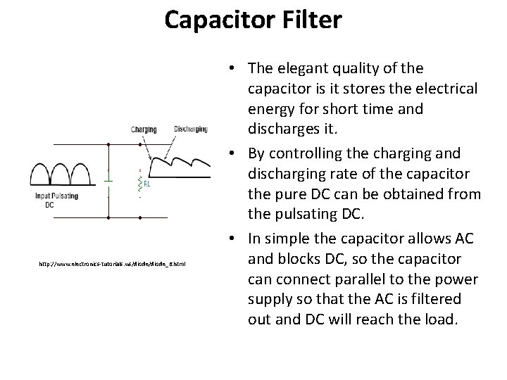
Capacitor Filter http: //www. electronics-tutorials. ws/diode_6. html • The elegant quality of the capacitor is it stores the electrical energy for short time and discharges it. • By controlling the charging and discharging rate of the capacitor the pure DC can be obtained from the pulsating DC. • In simple the capacitor allows AC and blocks DC, so the capacitor can connect parallel to the power supply so that the AC is filtered out and DC will reach the load.

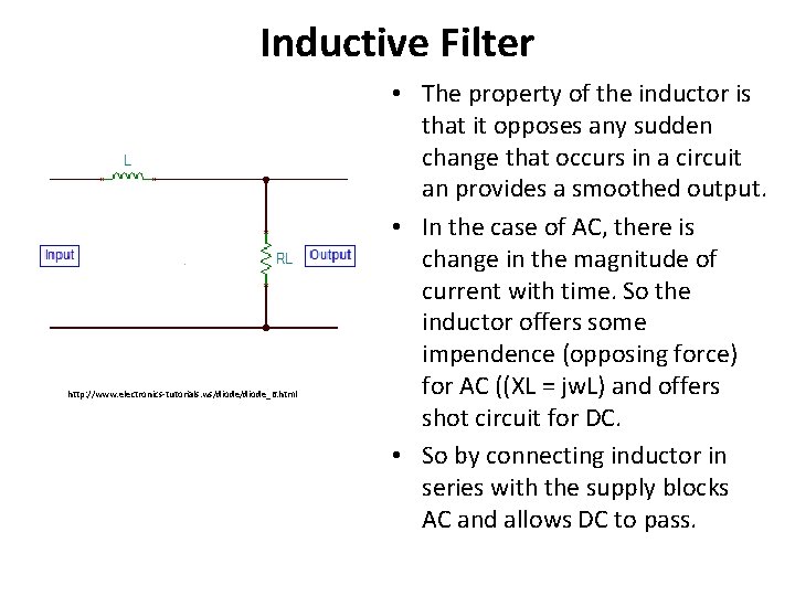
Inductive Filter http: //www. electronics-tutorials. ws/diode_6. html • The property of the inductor is that it opposes any sudden change that occurs in a circuit an provides a smoothed output. • In the case of AC, there is change in the magnitude of current with time. So the inductor offers some impendence (opposing force) for AC ((XL = jw. L) and offers shot circuit for DC. • So by connecting inductor in series with the supply blocks AC and allows DC to pass.

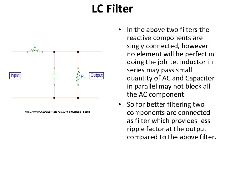
LC Filter http: //www. electronics-tutorials. ws/diode_6. html • In the above two filters the reactive components are singly connected, however no element will be perfect in doing the job i. e. inductor in series may pass small quantity of AC and Capacitor in parallel may not block all the AC component. • So for better filtering two components are connected as filter which provides less ripple factor at the output compared to the above filter.

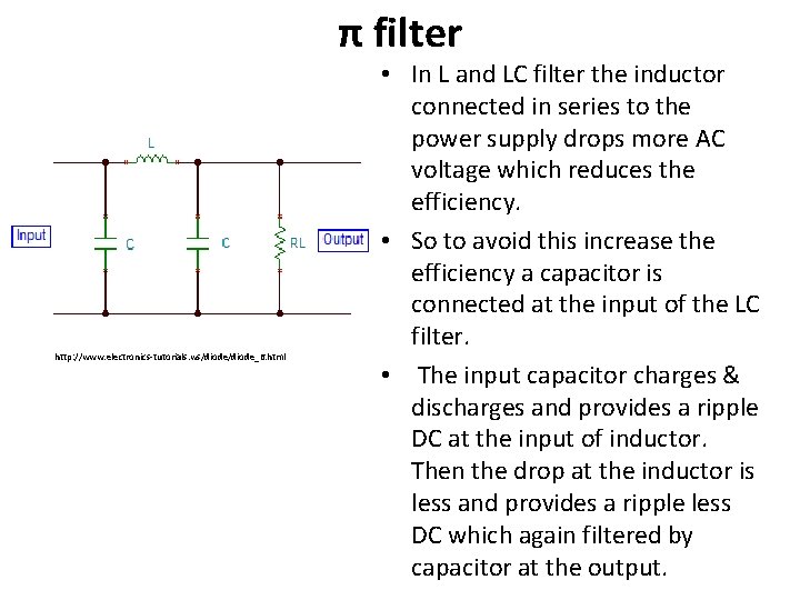
π filter http: //www. electronics-tutorials. ws/diode_6. html • In L and LC filter the inductor connected in series to the power supply drops more AC voltage which reduces the efficiency. • So to avoid this increase the efficiency a capacitor is connected at the input of the LC filter. • The input capacitor charges & discharges and provides a ripple DC at the input of inductor. Then the drop at the inductor is less and provides a ripple less DC which again filtered by capacitor at the output.