Carrier lifetime measurements with optical methods SPV and


![3. EBIC Method-Application Another two representative research papers [Ref-1]. H. J. Leamy, Charge collection 3. EBIC Method-Application Another two representative research papers [Ref-1]. H. J. Leamy, Charge collection](https://slidetodoc.com/presentation_image_h/154b0e5fa00fde245c8c25eedd268ae3/image-37.jpg)


- Slides: 41

Carrier lifetime measurements with optical methods: SPV and EBIC 15. 11. 2016 ELEC-L 3211 -Postgraduate Course in Micro and Nanosciences I V Haibing Huang (Huang. haibing@aalto. fi, haibing. huang@chinasunergy. com)

Outline 1. Fundamental Carrier lifetime/Recombination lifetime/Generation lifetime 2. Surface Photovoltage (SPV) Method 3. Electron Beam Induced Current (EBIC) Method 4. Summary 5. Homework

1. Fundamental For the introduction of this part, please refer to the lecture ppt of Juha and Camilla’s presentation.

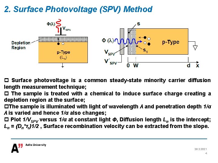
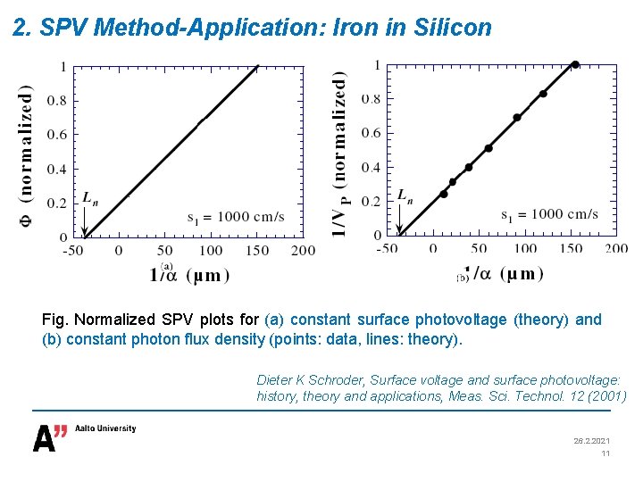
2. Surface Photovoltage (SPV) Method p Surface photovoltage is a common steady-state minority carrier diffusion length measurement technique; p The sample is treated with a chemical to induce surface charge creating a depletion region at the surface; p. The sample is illuminated with light of wavelength λ and penetration depth 1/α λ is varied and hence 1/α also changes; p Plot 1/VSPV versus 1/α at constant light Φ, Diffusion length Ln is the intercept; Ln = (Dn*τr)1/2 , Surface recombination velocity can be extracted from the slope. 26. 2. 2021 4

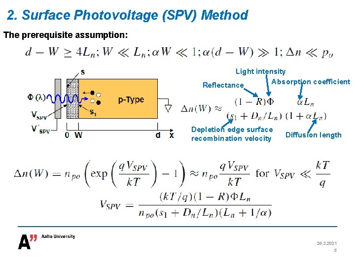
2. Surface Photovoltage (SPV) Method The prerequisite assumption: Light intensity Absorption coefficient Reflectance Depletion edge surface recombination velocity Diffusion length 26. 2. 2021 5

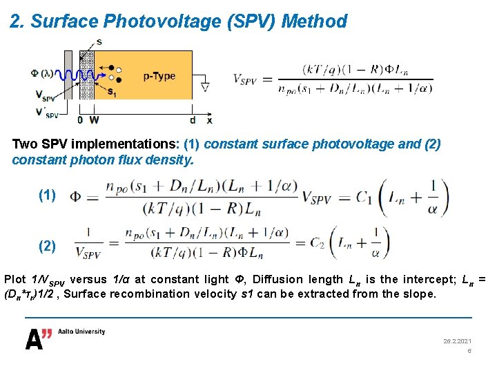
2. Surface Photovoltage (SPV) Method Two SPV implementations: (1) constant surface photovoltage and (2) constant photon flux density. (1) (2) Plot 1/VSPV versus 1/α at constant light Φ, Diffusion length Ln is the intercept; Ln = (Dn*τr)1/2 , Surface recombination velocity s 1 can be extracted from the slope. 26. 2. 2021 6

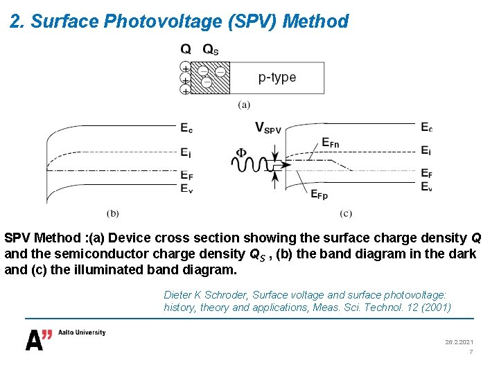
2. Surface Photovoltage (SPV) Method SPV Method : (a) Device cross section showing the surface charge density Q and the semiconductor charge density QS , (b) the band diagram in the dark and (c) the illuminated band diagram. Dieter K Schroder, Surface voltage and surface photovoltage: history, theory and applications, Meas. Sci. Technol. 12 (2001) 26. 2. 2021 7

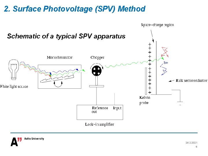
2. Surface Photovoltage (SPV) Method Schematic of a typical SPV apparatus 26. 2. 2021 8

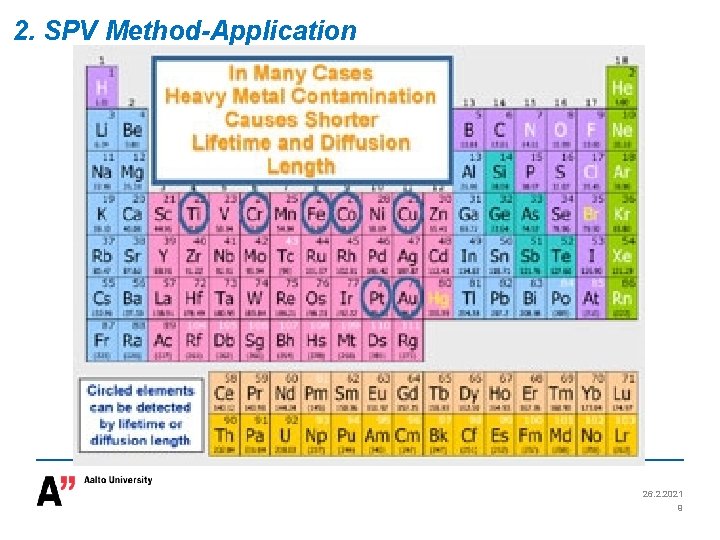
2. SPV Method-Application 26. 2. 2021 9

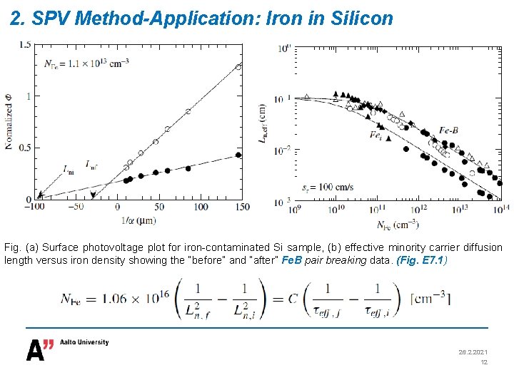
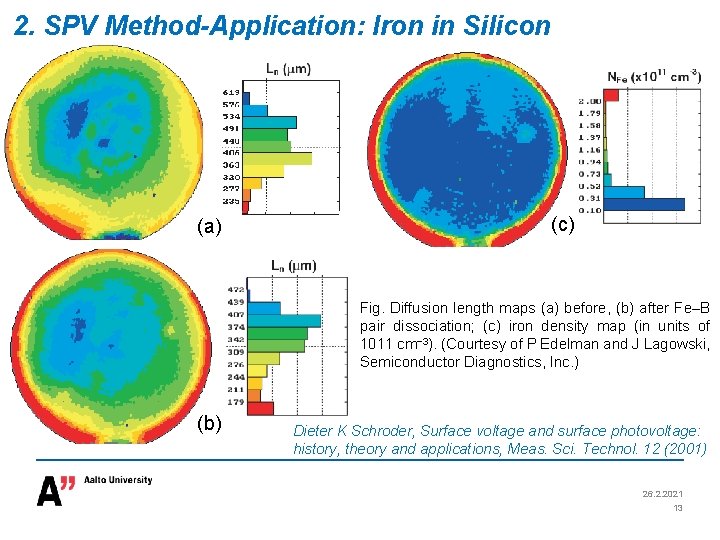
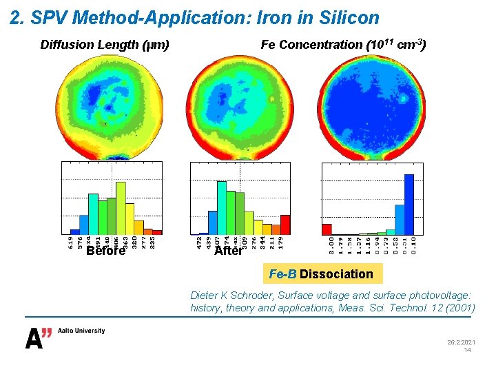
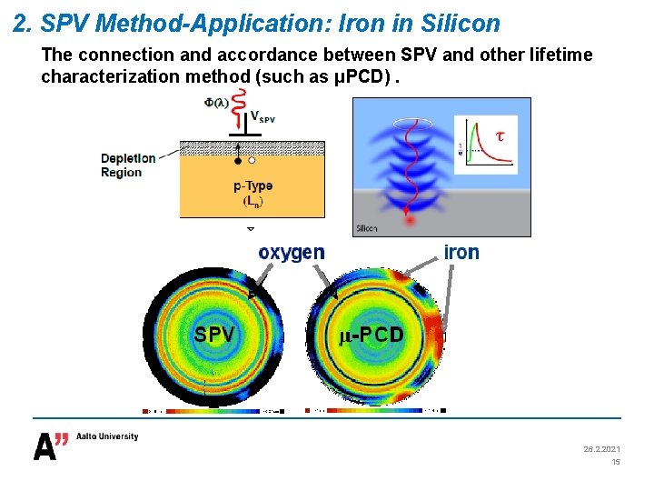
2. SPV Method-Application: Iron in Silicon Ø Iron in boron-doped p-type Si forms iron-boron pairs, Fe-B Ø When heated to 200°C/ 5 min or illuminated with bright light, Fe-B ⇒ interstitial iron (Fei), and substitutional boron (Bs) Ø Fei ⇒ Fe-B at room temperature after ~ 24 hours Ø The recombination properties of Fe-B differ from those of Fei Ø Use intense light to change Fe-B into Fei and Bs. Measuring the recombination lifetime before and after dissociation yields the iron density 26. 2. 2021 10

2. SPV Method-Application: Iron in Silicon Fig. Normalized SPV plots for (a) constant surface photovoltage (theory) and (b) constant photon flux density (points: data, lines: theory). Dieter K Schroder, Surface voltage and surface photovoltage: history, theory and applications, Meas. Sci. Technol. 12 (2001) 26. 2. 2021 11

2. SPV Method-Application: Iron in Silicon Fig. (a) Surface photovoltage plot for iron-contaminated Si sample, (b) effective minority carrier diffusion length versus iron density showing the “before” and “after” Fe. B pair breaking data. (Fig. E 7. 1) 26. 2. 2021 12

2. SPV Method-Application: Iron in Silicon (a) (c) Fig. Diffusion length maps (a) before, (b) after Fe–B pair dissociation; (c) iron density map (in units of 1011 cm− 3). (Courtesy of P Edelman and J Lagowski, Semiconductor Diagnostics, Inc. ) (b) Dieter K Schroder, Surface voltage and surface photovoltage: history, theory and applications, Meas. Sci. Technol. 12 (2001) 26. 2. 2021 13

2. SPV Method-Application: Iron in Silicon Diffusion Length (μm) Before Fe Concentration (1011 cm-3) After Fe-B Dissociation Dieter K Schroder, Surface voltage and surface photovoltage: history, theory and applications, Meas. Sci. Technol. 12 (2001) 26. 2. 2021 14

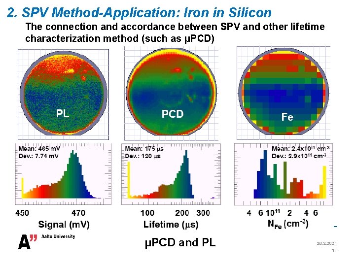
2. SPV Method-Application: Iron in Silicon The connection and accordance between SPV and other lifetime characterization method (such as μPCD). 26. 2. 2021 15

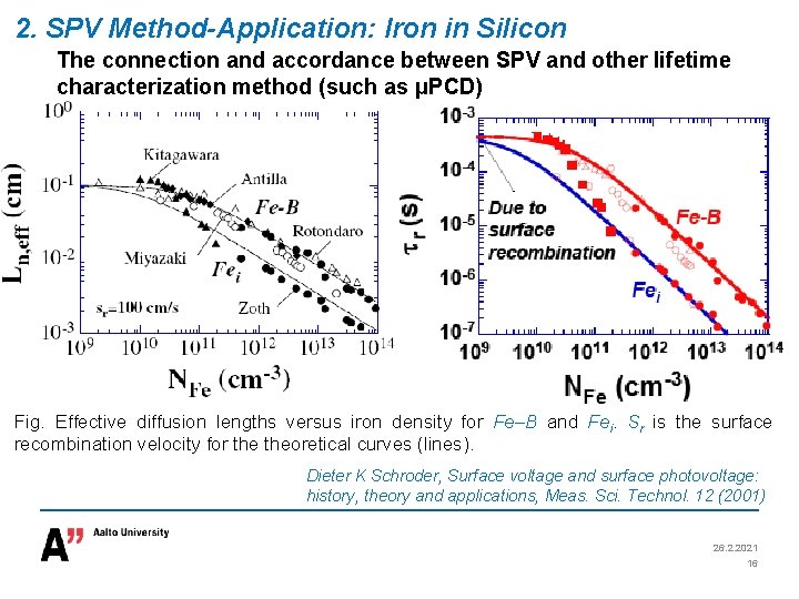
2. SPV Method-Application: Iron in Silicon The connection and accordance between SPV and other lifetime characterization method (such as μPCD) Fig. Effective diffusion lengths versus iron density for Fe–B and Fei. Sr is the surface recombination velocity for theoretical curves (lines). Dieter K Schroder, Surface voltage and surface photovoltage: history, theory and applications, Meas. Sci. Technol. 12 (2001) 26. 2. 2021 16

2. SPV Method-Application: Iron in Silicon The connection and accordance between SPV and other lifetime characterization method (such as μPCD) μPCD and PL 26. 2. 2021 17

2. SPV Method-Application: Iron in Silicon Another two representative research papers 1. G. Zoth and W. Bergholz, A Fast, Preparation-Free Method to Detect Iron in Silicon, J. Appl. Phys. 67, 6764– 6771, June 1990 and Macdonald et al. 2. D. H. Macdonald, L. J. Geerligs, and A. Azzizi, Iron Detection in Crystalline Silicon by Carrier Lifetime Measurements for Arbitrary Injection and Doping, J. Appl. Phys. 95, 1021– 1028, Feb. 2004) 26. 2. 2021 18

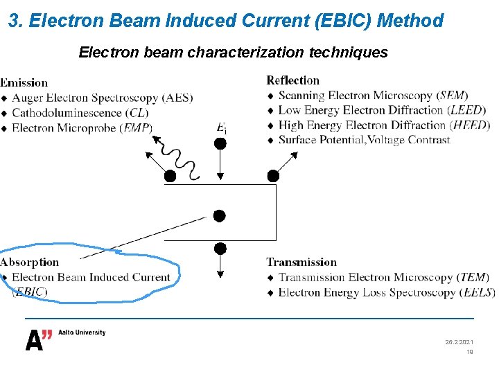
3. Electron Beam Induced Current (EBIC) Method Electron beam characterization techniques 26. 2. 2021 19

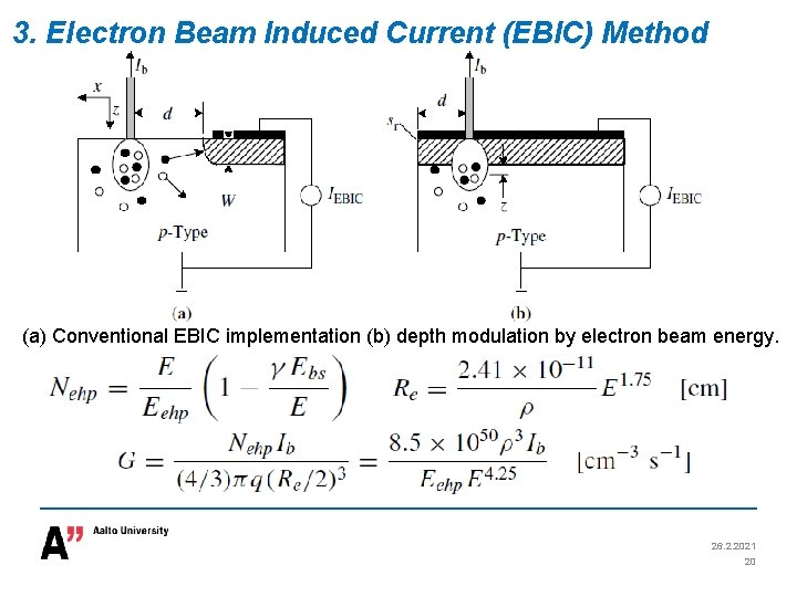
3. Electron Beam Induced Current (EBIC) Method (a) Conventional EBIC implementation (b) depth modulation by electron beam energy. 26. 2. 2021 20

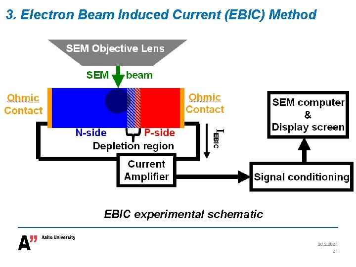
3. Electron Beam Induced Current (EBIC) Method EBIC experimental schematic 26. 2. 2021 21

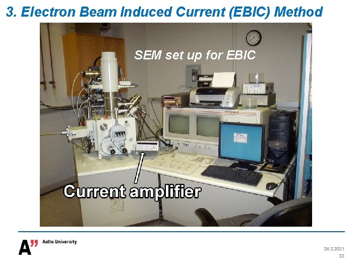
3. Electron Beam Induced Current (EBIC) Method SEM set up for EBIC 26. 2. 2021 22

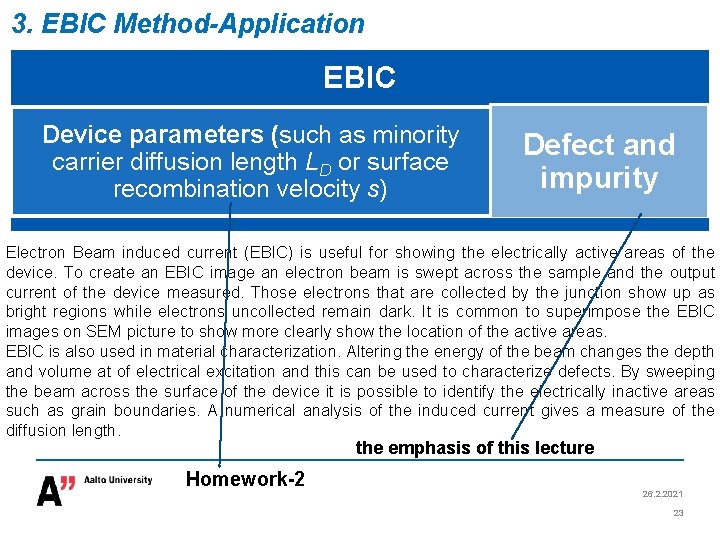
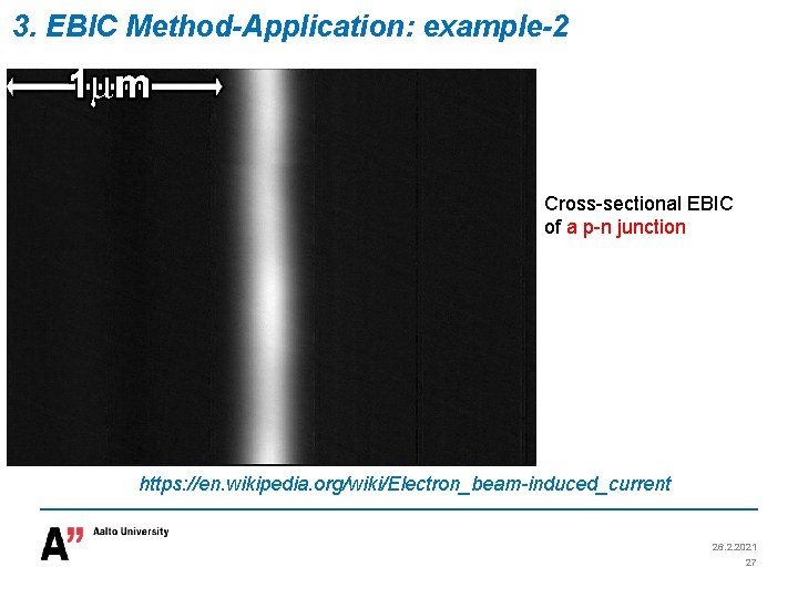
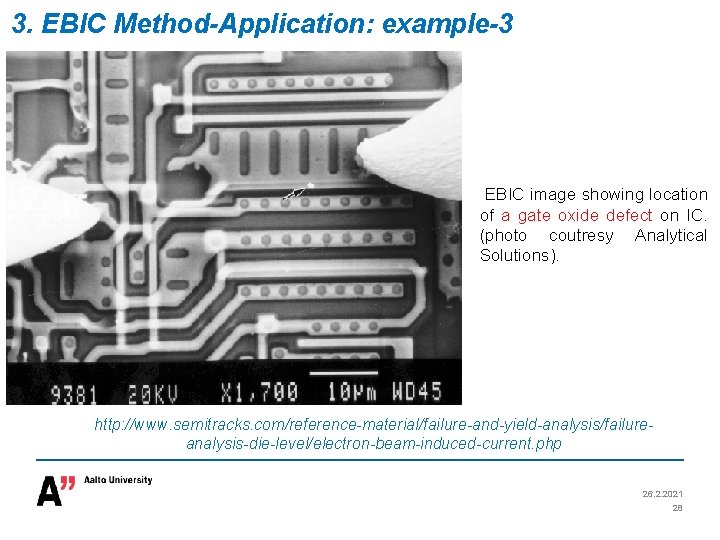
3. EBIC Method-Application EBIC Device parameters (such as minority carrier diffusion length LD or surface recombination velocity s) Defect and impurity Electron Beam induced current (EBIC) is useful for showing the electrically active areas of the device. To create an EBIC image an electron beam is swept across the sample and the output current of the device measured. Those electrons that are collected by the junction show up as bright regions while electrons uncollected remain dark. It is common to superimpose the EBIC images on SEM picture to show more clearly show the location of the active areas. EBIC is also used in material characterization. Altering the energy of the beam changes the depth and volume at of electrical excitation and this can be used to characterize defects. By sweeping the beam across the surface of the device it is possible to identify the electrically inactive areas such as grain boundaries. A numerical analysis of the induced current gives a measure of the diffusion length. the emphasis of this lecture Homework-2 26. 2. 2021 23

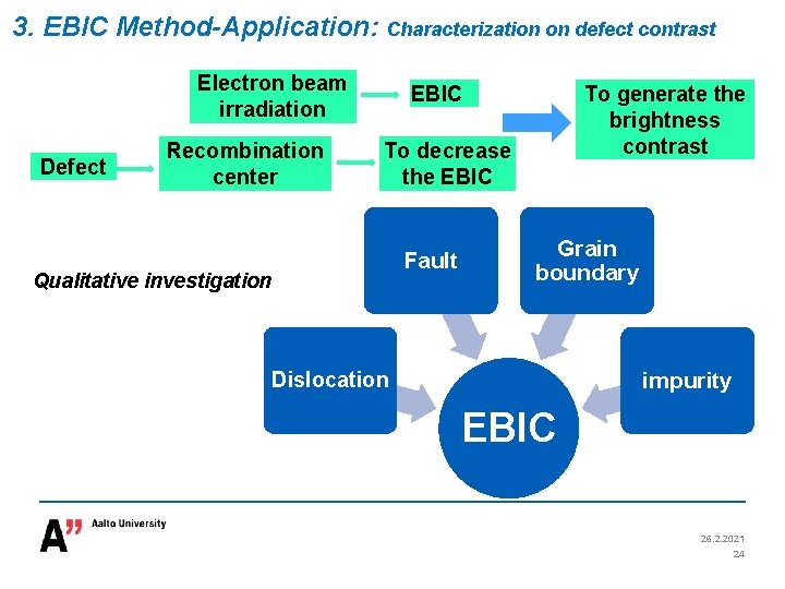
3. EBIC Method-Application: Characterization on defect contrast Electron beam irradiation Defect Recombination center To generate the brightness contrast EBIC To decrease the EBIC Fault Qualitative investigation Grain boundary impurity Dislocation EBIC 26. 2. 2021 24

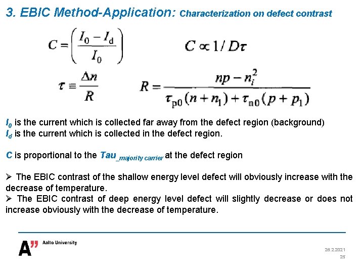
3. EBIC Method-Application: Characterization on defect contrast I 0 is the current which is collected far away from the defect region (background) Id is the current which is collected in the defect region. C is proportional to the Tau_majority carrier at the defect region Ø The EBIC contrast of the shallow energy level defect will obviously increase with the decrease of temperature. Ø The EBIC contrast of deep energy level defect will slightly decrease or does not increase obviously with the decrease of temperature. 26. 2. 2021 25

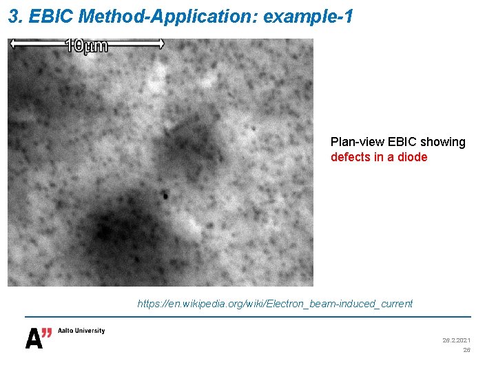
3. EBIC Method-Application: example-1 Plan-view EBIC showing defects in a diode https: //en. wikipedia. org/wiki/Electron_beam-induced_current 26. 2. 2021 26

3. EBIC Method-Application: example-2 Cross-sectional EBIC of a p-n junction https: //en. wikipedia. org/wiki/Electron_beam-induced_current 26. 2. 2021 27

3. EBIC Method-Application: example-3 EBIC image showing location of a gate oxide defect on IC. (photo coutresy Analytical Solutions). http: //www. semitracks. com/reference-material/failure-and-yield-analysis/failureanalysis-die-level/electron-beam-induced-current. php 26. 2. 2021 28

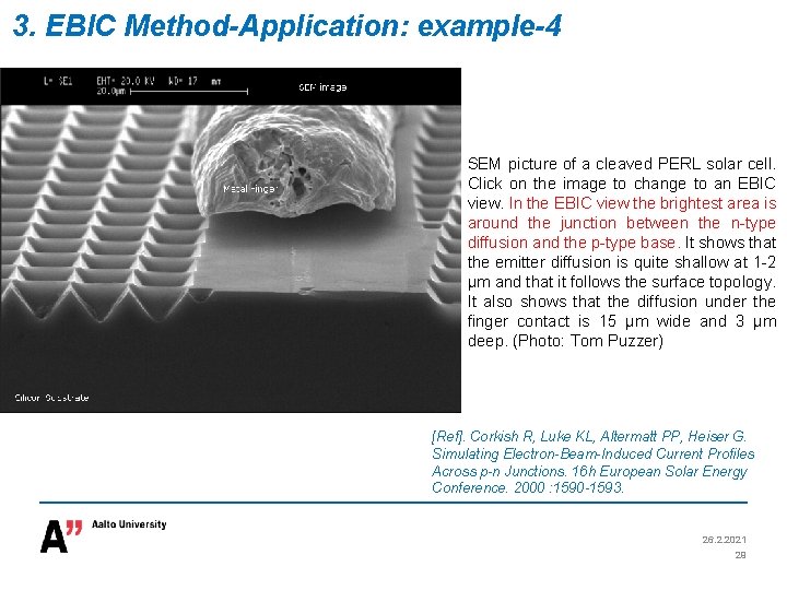
3. EBIC Method-Application: example-4 SEM picture of a cleaved PERL solar cell. Click on the image to change to an EBIC view. In the EBIC view the brightest area is around the junction between the n-type diffusion and the p-type base. It shows that the emitter diffusion is quite shallow at 1 -2 µm and that it follows the surface topology. It also shows that the diffusion under the finger contact is 15 µm wide and 3 µm deep. (Photo: Tom Puzzer) [Ref]. Corkish R, Luke KL, Altermatt PP, Heiser G. Simulating Electron-Beam-Induced Current Profiles Across p-n Junctions. 16 h European Solar Energy Conference. 2000 : 1590 -1593. 26. 2. 2021 29

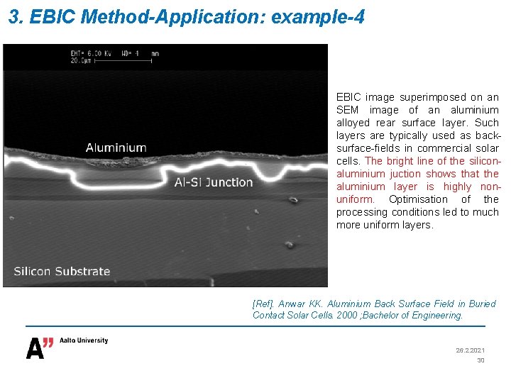
3. EBIC Method-Application: example-4 EBIC image superimposed on an SEM image of an aluminium alloyed rear surface layer. Such layers are typically used as backsurface-fields in commercial solar cells. The bright line of the siliconaluminium juction shows that the aluminium layer is highly nonuniform. Optimisation of the processing conditions led to much more uniform layers. [Ref]. Anwar KK. Aluminium Back Surface Field in Buried Contact Solar Cells. 2000 ; Bachelor of Engineering. 26. 2. 2021 30

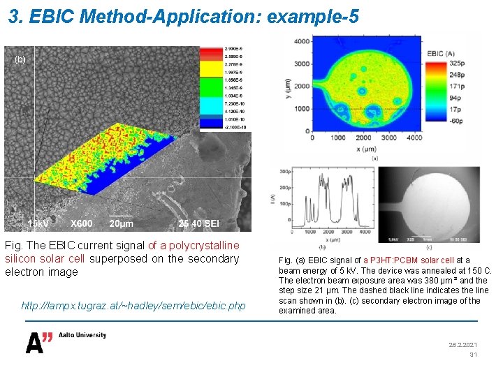
3. EBIC Method-Application: example-5 Fig. The EBIC current signal of a polycrystalline silicon solar cell superposed on the secondary electron image http: //lampx. tugraz. at/~hadley/sem/ebic. php Fig. (a) EBIC signal of a P 3 HT: PCBM solar cell at a beam energy of 5 k. V. The device was annealed at 150 C. The electron beam exposure area was 380 μm ² and the step size 21 μm. The dashed black line indicates the line scan shown in (b). (c) secondary electron image of the examined area. 26. 2. 2021 31

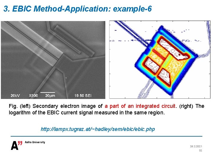
3. EBIC Method-Application: example-6 Fig. (left) Secondary electron image of a part of an integrated circuit. (right) The logarithm of the EBIC current signal measured in the same region. http: //lampx. tugraz. at/~hadley/sem/ebic. php 26. 2. 2021 32

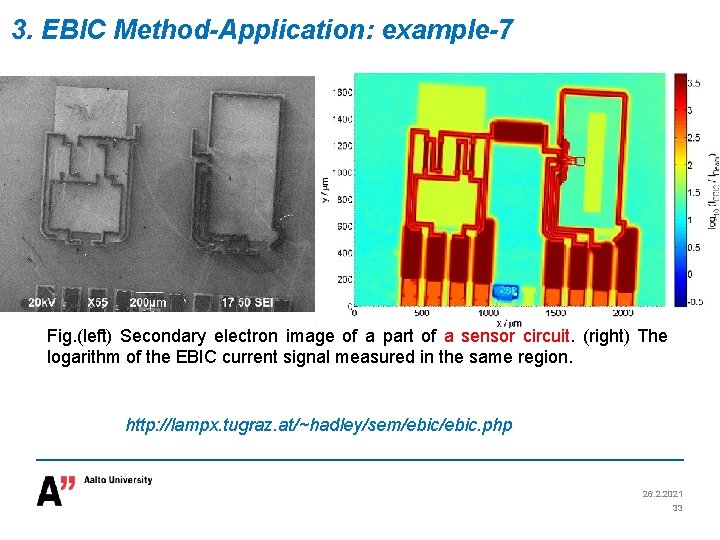
3. EBIC Method-Application: example-7 Fig. (left) Secondary electron image of a part of a sensor circuit. (right) The logarithm of the EBIC current signal measured in the same region. http: //lampx. tugraz. at/~hadley/sem/ebic. php 26. 2. 2021 33

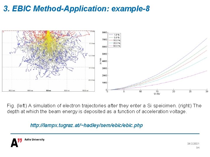
3. EBIC Method-Application: example-8 Fig. (left) A simulation of electron trajectories after they enter a Si speicimen. (right) The depth at which the beam energy is deposited as a function of acceleration voltage. http: //lampx. tugraz. at/~hadley/sem/ebic. php 26. 2. 2021 34

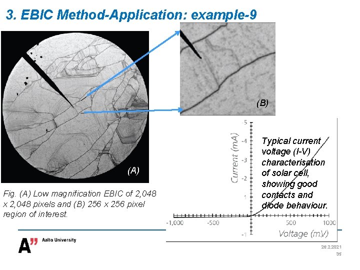
3. EBIC Method-Application: example-9 (B) (A) Fig. (A) Low magnification EBIC of 2, 048 x 2, 048 pixels and (B) 256 x 256 pixel region of interest. Typical current voltage (I-V) characterisation of solar cell, showing good contacts and diode behaviour. 26. 2. 2021 35

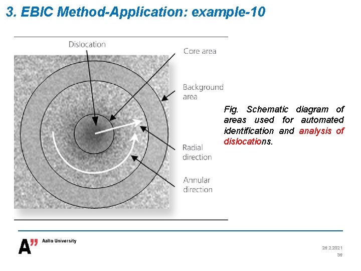
3. EBIC Method-Application: example-10 Fig. Schematic diagram of areas used for automated identification and analysis of dislocations. 26. 2. 2021 36
![3 EBIC MethodApplication Another two representative research papers Ref1 H J Leamy Charge collection 3. EBIC Method-Application Another two representative research papers [Ref-1]. H. J. Leamy, Charge collection](https://slidetodoc.com/presentation_image_h/154b0e5fa00fde245c8c25eedd268ae3/image-37.jpg)
3. EBIC Method-Application Another two representative research papers [Ref-1]. H. J. Leamy, Charge collection scanning electron microscopy, J. Appl. Phys. 53, (1982). [Ref-2]. Piet Reuter, Thomas Rath, Achim Fischereder, Gregor Trimmel, and Peter Hadley, Electron Beam-Induced Current (EBIC) in solution-processed solar cells, Scanning Vol. 33. pp. 1 -6 (2011). 26. 2. 2021 37

4. Summary ØThe steady-state surface photovoltage method determines the minority carrier diffusion length using optical excitation. SPV is an attractive technique, because (1) it is nondestructive and contactless, (2) sample preparation is simple (no contacts, junctions, or high temperature processing required), (3) it is a steady-state method relatively immune to the slow trapping and detrapping effects that can influence transient measurements, and (4) the equipment is commercially available. ØElectron beam induced current is used to measure minority carrier diffusion length, minority carrier lifetime, and defect distribution. In contrast to photons that typically create one ehp pair upon absorption, an absorbed electron of energy E creates electron-hole pairs. 38

5. Home work-1: Problem 7. 11 (page 471): Generate and plot surface photovoltage (SPV) curves of versus 1/α for a p-Si substrate using the following parameters: (i) Ln =100 μm, s 1 =100 cm/s; (ii) Ln =100 μm, s 1 =10, 000 cm/s; (iii) Ln =10 μm, s 1 =100 cm/s. Plot all three curves on the same figure. Give appropriate units to and 1/α. Use Eqs. (7. 54), (7. 60), and (7. 63), Dn =30 cm/s, n(W)=1010 cm− 3, 0. 7≤λ≤ 1. 05 μm. Then determine Ln and s 1 from these SPV plots to see if you obtain the starting values. 39

5. Home work-2 (Optional): Read the following two research papers and try to understand how EBIC method measures the minority carrier diffusion length. [1]. A. Eisenbeiss, H. Heinrich, A. Jakubowicz, W. Maurer, L. Palmetshofer, H. M. Preier, K. H. Bachem, and H. Böttner, Investigation of diffusion length and lifetime in lead chalcogenides by electron‐beaminduced‐current measurements at low temperatures, Journal of Applied Physics 56, 362 (1984); [2]. DIMITRIS E. IOANNOU AND CHARALABOS A. DIMITRIADIS, A SEM-EBIC Minority-Carrier Diffusion-Length Measurement Technique, IEEE Transactions on Electron Devices, 1982, 29(3): 445 -450. 40

26. 2. 2021 41