ARM Based microcontrollers Asst Prof Dr Alper MAN
ARM Based microcontrollers Asst. Prof. Dr. Alper ŞİŞMAN
ARM Cortex Processors • ARM Cortex-A family (v 7 -A): – Applications processors for full OS and 3 rd party applications • ARM Cortex-R family (v 7 -R): – Embedded processors for real-time signal processing, control applications • ARM Cortex-M family (v 7 -M): – Microcontroller-oriented processors for MCU and So. C applications
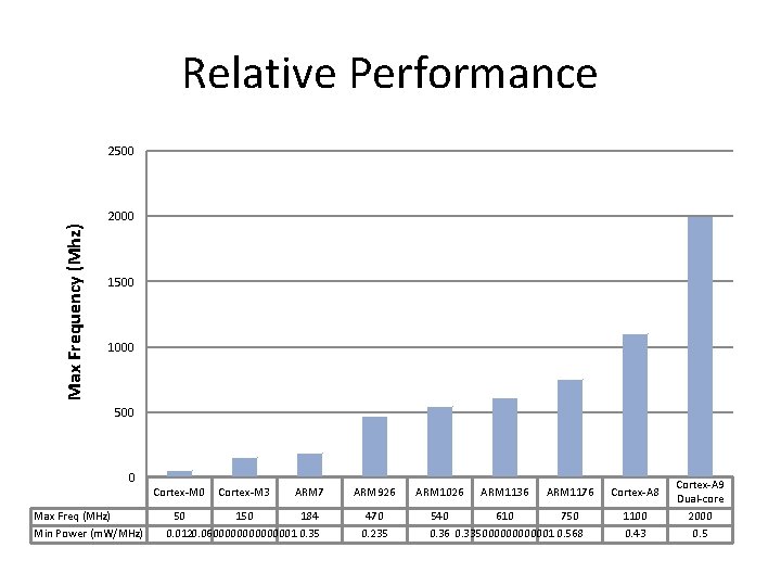
Relative Performance Max Frequency (Mhz) 2500 2000 1500 1000 500 0 Max Freq (MHz) Min Power (m. W/MHz) Cortex-M 0 Cortex-M 3 ARM 7 50 184 0. 0120. 0600000001 0. 35 ARM 926 470 0. 235 ARM 1026 ARM 1136 ARM 1176 540 610 750 0. 36 0. 3350000001 0. 568 Cortex-A 8 1100 0. 43 Cortex-A 9 Dual-core 2000 0. 5
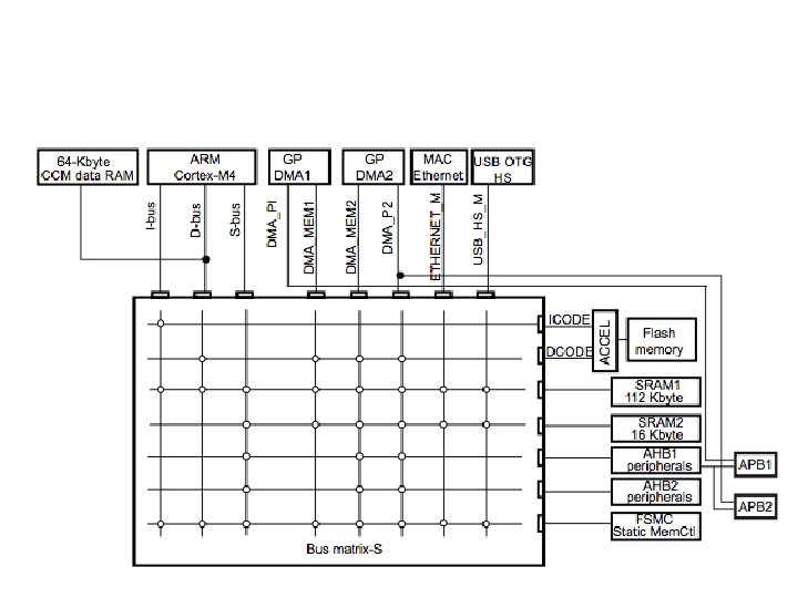
STM 32 F 40 x HW Architecture • The main system consists of 32 -bit multilayer Advanced High-Speed bus (AHB) matrix that interconnects 8 master units to 7 slaves. • The bus matrix provides access from a master to a slave, enabling concurrent access and efficient operation even when several highspeed peripherals work simultaneously. • There are 2 bus structure connected to the matrix: AHB and APB systems.
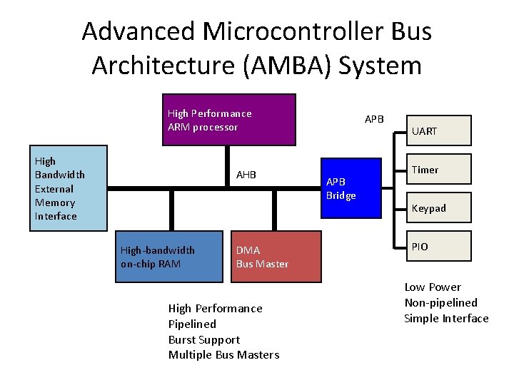
Advanced Microcontroller Bus Architecture (AMBA) System High Performance ARM processor High Bandwidth External Memory Interface AHB High-bandwidth on-chip RAM DMA Bus Master High Performance Pipelined Burst Support Multiple Bus Masters APB Bridge UART Timer Keypad PIO Low Power Non-pipelined Simple Interface
• I-Bus: Instruction bus of the ARM core. This bus is used by the core to fetch instructions. The target of this bus is a memory containing code. • D-Bus: Databus of ARM core. This bus is used by the core for literal load and debug access. The target of this bus is a memory containing code or data. • S-Bus: System bus. This bus is used to access data located in a peripheral or in SRAM. Instructions may also be fetch on this bus (less efficient than ICode). The targets of this bus are the internal SRAM 1, SRAM 2 and SRAM 3, the AHB 1 peripherals including the APB peripherals, the AHB 2 peripherals and the external memories through the FSMC/FMC.
Direct Memory Access (DMA) • A feature of modern computers that allows certain hardware subsystems within the computer to access system memory independently of the central processing unit (CPU). CPU only initiates the process and DMA controller sends an interrupt when operation is done. • DMA Memory Bus: Direct memory access bus. It is used by the DMA to perform transfer to/from memories. The targets of this bus are data memories. • DMA peripheral bus: This bus is used by the DMA to access AHB peripherals or to perform memory-tomemory transfers. The targets of this bus are the AHB and APB peripherals plus data memories.
Other DMA blocks • Ethernet DMA BUS: This bus is used by the Ethernet DMA to load/store data to a memory. The targets of this bus are data memories. • USB OTG HS DMA bus: This bus is used by the USB OTG DMA to load/store data to a memory. The targets of this bus are data memories.
Bridges • AHB/APB Bridges: The two AHB/APB bridges, APB 1 and APB 2, provide full synchronous connections between the AHB and the two APB buses, allowing flexible selection of the peripheral frequency.
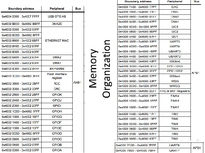
Memory Organization
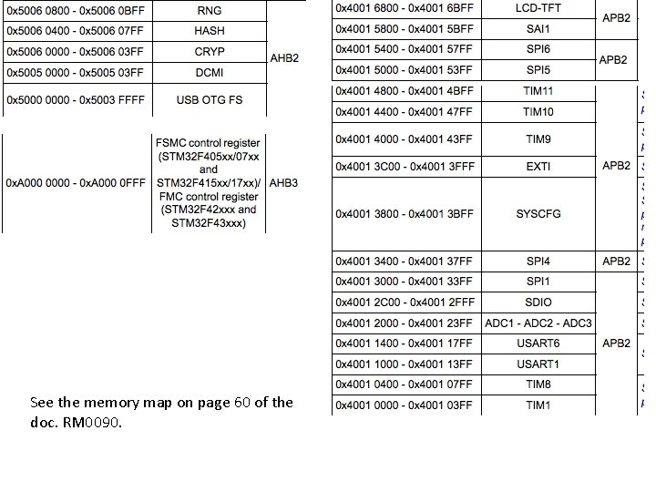
See the memory map on page 60 of the doc. RM 0090.
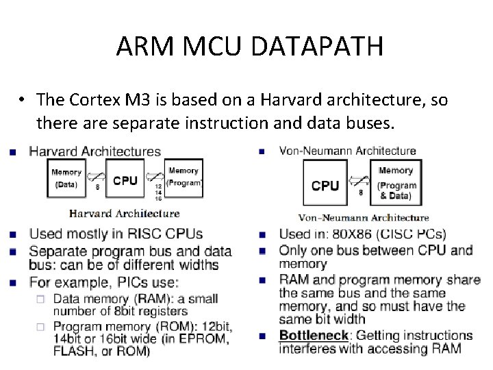
ARM MCU DATAPATH • The Cortex M 3 is based on a Harvard architecture, so there are separate instruction and data buses.
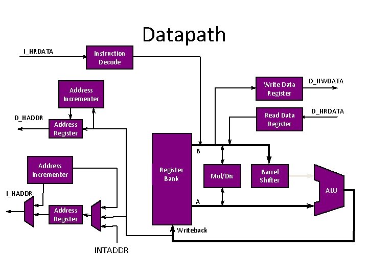
Datapath I_HRDATA Instruction Decode Write Data Register Address Incrementer D_HADDR D_HWDATA D_HRDATA Read Data Register Address Register B Address Incrementer Register Bank I_HADDR Mul/Div A Address Register Writeback INTADDR Barrel Shifter ALU
• Instructions come in along the AHB instruction read bus to the decode stage. I_HADDR is the Address bus on the instruction side bus. • So there are separate read data and write data registers and a data address bus. • All data processing is performed on registers, not directly on memory locations. So we can say something like ADD r 0, r 1, LSL#1. R 1 comes along both A and B buses, <and B can be shifted in Barrel shifter>
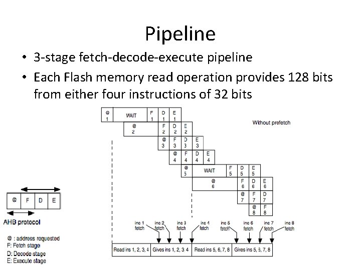
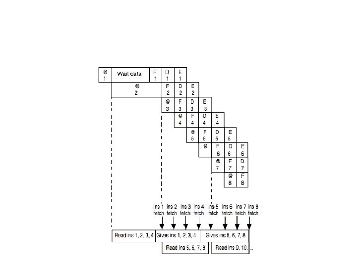
Pipeline • 3 -stage fetch-decode-execute pipeline • Each Flash memory read operation provides 128 bits from either four instructions of 32 bits
Adaptive real-time memory accelerator • To release the processor full performance, the accelerator implements an instruction prefetch queue and branch cache. • Prefetch on the I-Code bus can be used to read the next sequential instruction line from the Flash memory while the current instruction line is being requested by the CPU.
Reset & Clock Control • There are three types of reset, defined as system Reset (RCC clock control & status register (RCC_CSR). ), power Reset and backup domain Reset (RCC Backup domain control register (RCC_BDCR)). • Clocks : The clock controller (RCC) provides a high degree of flexibility to the application and, guarantee the appropriate frequency for peripherals that need a specific clock like Ethernet, USB OTG FS and HS, I 2 S and SDIO. • Each Hardware block has to be clocked before using • The maximum frequency of the AHB domain is 168 MHz. The maximum allowed frequency of the high-speed APB 2 domain is 84 MHz. The maximum allowed frequency of the low-speed APB 1 domain is 42 MHz • See all registers about RCC on page 211 of the doc. RM 0090
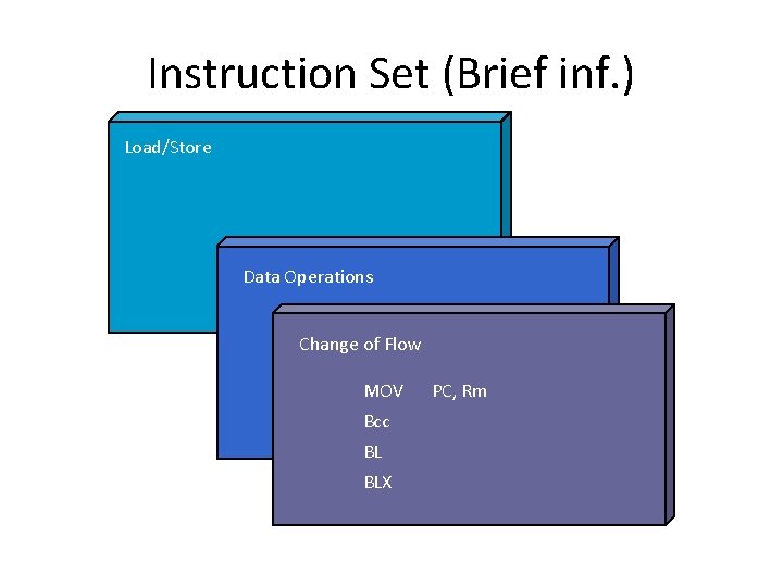
Instruction Set (Brief inf. ) Load/Store Data Operations Change of Flow MOV Bcc BL BLX PC, Rm
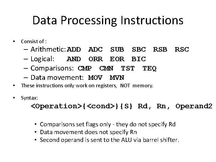
Data Processing Instructions • Consist of : • These instructions only work on registers, NOT memory. • Syntax: – Arithmetic: ADD ADC SUB SBC RSB RSC – Logical: AND ORR EOR BIC – Comparisons: CMP CMN TST TEQ – Data movement: MOV MVN <Operation>{<cond>}{S} Rd, Rn, Operand 2 • Comparisons set flags only - they do not specify Rd • Data movement does not specify Rn • Second operand is sent to the ALU via barrel shifter.
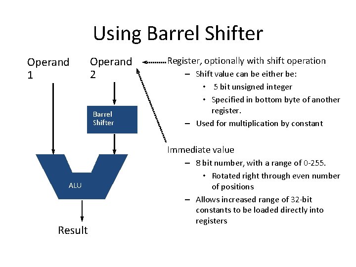
Using Barrel Shifter Operand 1 Operand 2 Barrel Shifter Register, optionally with shift operation – Shift value can be either be: • 5 bit unsigned integer • Specified in bottom byte of another register. – Used for multiplication by constant Immediate value ALU Result – 8 bit number, with a range of 0 -255. • Rotated right through even number of positions – Allows increased range of 32 -bit constants to be loaded directly into registers
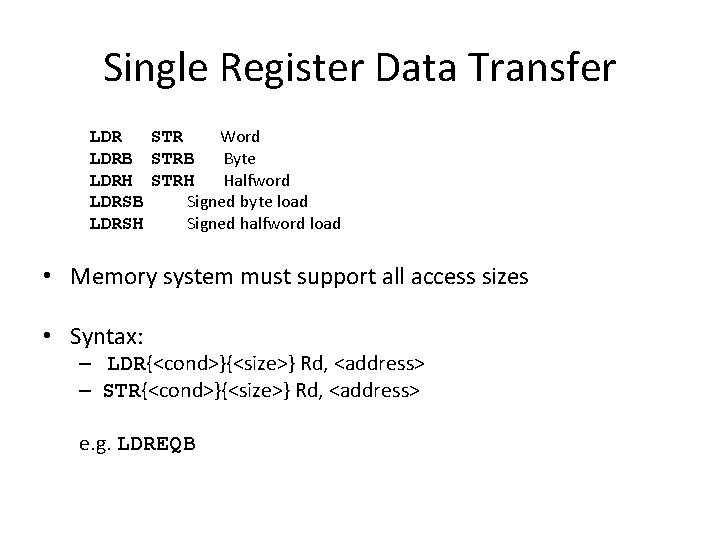
Single Register Data Transfer LDR STR Word LDRB STRB Byte LDRH STRH Halfword LDRSB Signed byte load LDRSH Signed halfword load • Memory system must support all access sizes • Syntax: – LDR{<cond>}{<size>} Rd, <address> – STR{<cond>}{<size>} Rd, <address> e. g. LDREQB
- Slides: 24