OVERVIEW OF PIC AVR FAMILY OF MICROCONTROLLERS ARM


 Plastic Leaded Chip")
")


 is 13 bit and capable of addressing an")
")
")


 Only available in")

 with 9")


 is a circuit that provides a predictable,")


- Slides: 36
OVERVIEW OF PIC & AVR FAMILY OF MICROCONTROLLERS & ARM PROCESSORS APPENDIX 1, INTRODUCTION TO EMBEDDED SYSTEMS BY SHIBU K. V
Microchip PIC • PIC is a family of Harvard architecture microcontroller made by Microchip Technology. The name PIC initially referred to "Peripheral Interface Controller“. PIC microcontrollers were the first RISC microcontroller. • PICs are popular with both industrial developers and hobbyists alike due to their low cost, wide availability, large user base, extensive collection of application notes, availability of low cost or free development tools, and serial programming (and re-programming with flash memory) capability.
Two Different Architectures
PIC Microcontroller product family • 8 -bit microcontrollers – – – PIC 10 PIC 12 PIC 14 PIC 16 PIC 17 PIC 18 • 16 -bit microcontrollers – PIC 24 F – PIC 24 H • 32 -bit microcontrollers – PIC 32 • 16 -bit digital signal controllers – ds. PIC 30 – ds. PIC 33 F
PIC Microcontroller groups • Baseline – – Based on original PIC architecture Support 12 bit instructions with limited features Available in 6 -40 pin packages 6 pin 10 F series, 8 pin 12 F series, some other 12 F and 16 F series falls under this category • Mid range – Extension to baseline architecture with added features like support for interrupts, on chip peripherals, increased memory. – Instruction set for this architecture is 14 bit wide – Available in 8 to 64 pin packages and operating voltage in the range 1. 8 v to 5. 5 v. – Some 12 F, 16 F series come under this category • High Performance – – – PIC 18 F, J & K series come under this category. Memory density is very high. Builtin support for advanced peripherals like USB, CAN, etc. Instruction set for this architecture is 16 bit wide Capable of delivering a speed of 16 MIPS
PIC Microcontroller product family 4 • The F in a name generally indicates the PICmicro uses flash memory and can be erased electronically. • The C generally means it can only be erased by exposing the die to ultraviolet light (which is only possible if a windowed package style is used). An exception to this rule is the PIC 16 C 84 which uses EEPROM and is therefore electrically erasable. 1:
Why use PIC 16 F 877? Why PIC 16 F 877 A is very popular? This is because PIC 16 F 877 A is very cheap. Apart from that it is also very easy to be assembled. Additional components that you need to make this IC work is just a 5 V power supply adapter, a 20 MHz crystal oscillator and 2 units of 22 p. F capacitors. What is the advantages of PIC 16 F 877 A? This IC can be reprogrammed and erased up to 10, 000 times. Therefore it is very good for new product development phase. What is the disadvantages of PIC 16 F 877 A? This IC has no internal oscillator so you will need an external crystal of other clock source.
Features of PIC 16 F 877 Key Features PIC 16 F 877 MAX Operating Frequency 20 MHz FLASH Program Memory (14 -bit words) 8 K Data Memory (bytes) 368 EEPROM Data Memory (bytes) 256 8 I/O Ports RA 0 -5 (6) RB 0 -7 (8) RC 0 -7 (8) RD 0 -7 (8) RE 0 -2 (3) Timers 3 CCP 2 Serial Communications MSSP, USART Parallel Communications PSP 10 -bit Analog-to-Digital Module 8 Channels Instruction Set 35 Instructions Pins (DIP) 40 Pins
Pin Diagram of PIC 16 F 877 Quad Flat Package (QFP) Plastic Leaded Chip Carrier Package (PLCC)
Pin Diagram of PIC 16 F 877 • Plastic dual in-line package (DIP)
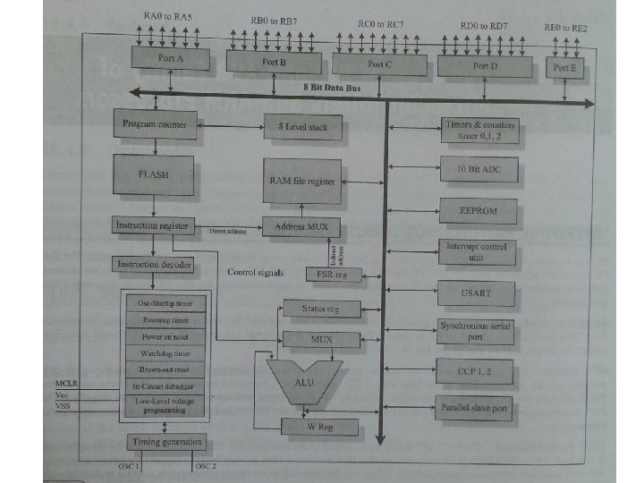
PIC 16 F 877 Architecture
PIC 16 F 877 Internal Block Diagram • The basic architecture of PIC 16 F 877 consists of Program memory, file registers and RAM, ALU and CPU registers. PIC 16 F 877 Internal Block Diagram
Memory of the PIC 16 F 877 • divided into 3 types of memories: 1. Program Memory – A memory that contains the program (which we had written), after we've burned it. As a reminder, Program Counter executes commands stored in the program memory, one after the other. 2. Data Memory – This is RAM memory type, which contains a special registers like SFR (Special Function Register) and GPR (General Purpose Register). The variables that we store in the Data Memory during the program are deleted after we turn of the micro. These two memories have separated data buses, which makes the access to each one of them very easy. 3. Data EEPROM (Electrically Erasable Programmable Read-Only Memory) – A memory that allows storing the variables as a result of burning the written program.
…cont’d • Each one of them has a different role. Program Memory and Data Memory two memories that are needed to build a program, and Data EEPROM is used to save data after the microcontroller is turn off.
PIC 16 F 877 A Registers • Some CPU Registers: • W • PC • FSR • IDF • PCLATH • STATUS
W Register • W, the working register, is used by many instructions as the source of an operand. This is similar to accumulator in 8051. • It may also serve as the destination for the result of the instruction execution. It is an 8 bit register. W, working register
18
Program Counter • Program Counter (PC) is 13 bit and capable of addressing an 8 K word x 14 bit program memory space. • PC keeps track of the program execution by holding the address of the current instruction. It is automatically incremented to the next instruction during the current instruction execution. • Program Counter Stack an independent 8 -level stack is used for the program counter. As the PC is 13 -bit, the stack is organized as 8 x 13 bit registers. When an interrupt occurs, the PC is pushed onto the stack. When the interrupt is being served, other interrupts remain disabled. Hence, other 7 registers of the stack can be used for subroutine calls within an interrupt service routine or within the mainline program.
• FSR Register • (File Selection Register, address = 04 H, 84 H) is an 8 -bit register used as data memory address pointer. This is used in indirect addressing mode. • INDF Register • (INDirect through FSR, address = 00 H, 80 H) INDF is not a physical register. Accessing INDF is actually access the location pointed to by FSR in indirect addressing mode.
• PCL Register • (Program Counter Low Byte, address =02 H, 82 H) PCL is actually the lower 8 -bits of the 13 -bit Program Counter. This is a both readable and writable register. • PCLATH Register • (Program Counter LATc. H, address = 0 AH, 8 AH) PCLATH is a 8 -bit register which can be used to decide the upper 5 -bits of the PC. PCLATH is not the upper 5 bits of the PC. PCLATH can be read from or written to without affecting the PC. The upper 3 bits of PCLATH remain zero and they serve no purpose. When PCL is written to, the lower 5 bits of PCLATH are automatically loaded to the upper 5 bits of the PC, as shown below:
• In order to start programming and build automated system, there is no need to study all the registers of the memory map, but only a few most important ones: – STATUS register – changes/moves from/between the banks. – PORT registers – assigns logic values (“ 0”/” 1”) to the ports – TRIS registers – data direction register (input/output)
STATUS Register • Is an 8 -bit register that stores the status of the processor. • In most cases, this register is used to switch between the banks (Register Bank Select), but also has other capabilities. • • IRP - Register Bank Select bit. RP 1: RP 0: - Register Bank Select bits. TO: Time-out bit Used in conjunction with PIC’s sleep mode PD: Power-down bit Z: Zero bit DC: Digit carry/borrow bit C: Carry/borrow bit
STATUS Register
PIC 16 F 877 Peripheral features 1. I/O Ports: – PIC 16 F 877 has 5 I/O ports: – PORT A has 6 bit wide, Bidirectional – PORT B, C, D have 8 bit wide, Bidirectional – PORT E has 3 bit wide, Bidirectional – In addition, they have the following alternate functions:
PIC 16 F 877 Peripherals – Each port has 2 control registers: – TRISx sets whether each pin is an input(1) or output(0) – PORTx sets their output bit levels or contain their input bit levels. – Pin functionality “overloaded” with other features. – Most pins have 25 m. A source/sink thus it can drive LEDs directly.
PIC 16 F 877 Peripherals 2. Analog to Digital Converter (ADC) Only available in 14 bit and 16 bit cores Fs (sample rate) < 54 KHz The result is a 10 bit digital number Can generate an interrupt when ADC conversion is done The A/D module has 4 registers: Multiplexed 8 channel inputs A/D Result High Register (ADRESH) A/D Result Low Register (ADRESL) A/D Control Register 0 (ADCON 0) A/D Control Register 1 (ADCON 1) Must wait T acq to change up sampling capacitor. Can take a reference voltage different from that of
PIC 16 F 877 Peripherals 3. Timer/counter modules – Generate interrupts on timer overflow – Can use external pins as clock in/ clock out (ie. for counting events or using a different Fosc) – There are 3 Timer/counter modules: • Timer 0: 8 -bit timer/counter with 8 -bit pre-scaler • Timer 1: 16 -bit timer/counter with 8 -bit pre-scaler, can be incremented during SLEEP via external crystal/clock • Timer 2: 8 -bit timer/counter with 8 -bit period register, pre-scaler and post-scaler.
PIC 16 F 877 Peripherals 4. Universal Synchronous Asynchronous Receiver Transmitter (USART/SCI) with 9 -bit address detection. – Asynchronous communication: UART (RS 232 serial) • Can do 300 bps – 115 kbps • 8 or 9 bits, parity, start and stop bits, etc. • Outputs 5 V needs a RS 232 level converter (e. g MAX 232)
PIC 16 F 877 Peripherals • Synchronous communication: i. e with clock signal • SPI = Serial Peripheral Interface – – 3 wire: Data in, Data out, Clock Master/Slave (can have multiple masters) Very high speed (1. 6 Mbps) Full speed simultaneous send and receive (Full duplex) • I 2 C = Inter IC – 2 wire: Data and Clock – Master/Slave (Single master only; multiple masters clumsy) – Lots of cheap I 2 C chips available; typically < 100 kbps
PIC 16 F 877 Peripherals 5. Capture, Compare, PWM modules – Capture is 16 -bit, max. resolution is 12. 5 ns – Compare is 16 -bit, max. resolution is 200 ns – PWM max. resolution is 10 -bit 6. Synchronous Serial Port (SSP) with SPITM (Master mode) and 12 CTM (Master/Slave) 7. Parallel Slave Port (PSP) 8 -bits wide, with external RD, WR and CS controls
PIC RESET ACTIONS 1. 2. 3. 4. POR BOR Watch Dog Reset External Reset
P-O-R • A power-on reset (Po. R) is a circuit that provides a predictable, regulated voltage to a microprocessor or microcontroller with the initial application of power. • The Po. R system ensures that the microprocessor or microcontroller will start in the same condition every time that it is powered up. • A well-designed Po. R circuit can ensure that when power is applied to a computer, it will start up properly every time (or almost every time), and will never (or rarely) freeze up right away. • This feature not only saves the user a great deal of frustration, but it offers a last resort in case of a stubborn system crash: the so-called cold boot, where the computer is completely powered-down for a minute or two, and then powered-up all over again. Ref: http: //whatis. techtarget. com/definition/power-on-reset-Po. R
BOR • BOR is available only in PIC 16 C 66 and 16 C 74 • On-chip Brown-out Reset circuitry places the device into reset when the device voltage falls below a trip point (4 v) • This ensures that the device does not continue program execution outside the valid operation range of the device.
• Watch Dog Reset – Occurs when the watch dog timer overflows • External Reset – A pulse at the reset pin (MCLR) can reset the microcontroller from an external source
SUMMARY 1 • The microcontroller contains a processor, memory and input/output devices • The program is stored in ROM memory in numbered locations (addresses) • The P 16 F 877 stores a maximum of 8 k 14 instructions in flash ROM • The P 16 FXXX family uses only 35 instructions • The P 16 F 877 has 368 bytes of RAM and 5 ports (33 I/O pins) • The ports act as buffers between the MCU and external systems • The program is executed in sequence, unless there is a jump instruction • The program counter tracks the current instruction address