Adder wrapup Lecture 14 2017 Purpose of todays

- Slides: 19

Adder wrap-up Lecture 14 2017

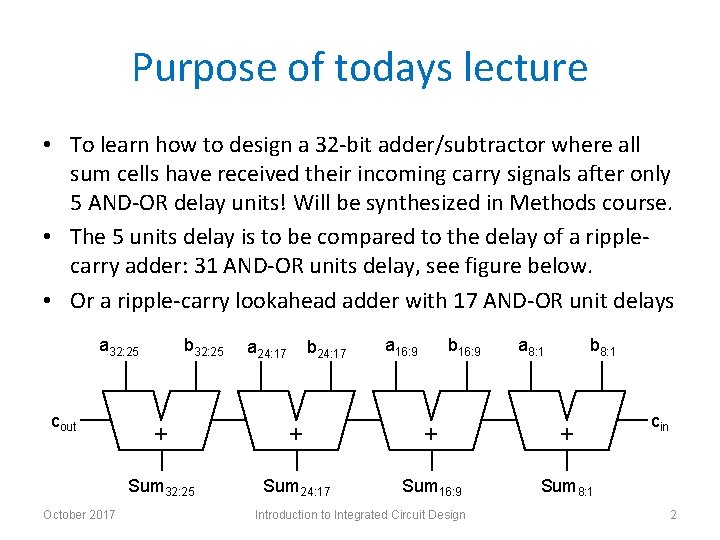
Purpose of todays lecture • To learn how to design a 32 -bit adder/subtractor where all sum cells have received their incoming carry signals after only 5 AND-OR delay units! Will be synthesized in Methods course. • The 5 units delay is to be compared to the delay of a ripplecarry adder: 31 AND-OR units delay, see figure below. • Or a ripple-carry lookahead adder with 17 AND-OR unit delays a 32: 25 cout October 2017 b 32: 25 a 24: 17 b 24: 17 a 16: 9 b 16: 9 a 8: 1 b 8: 1 + + Sum 32: 25 Sum 24: 17 Sum 16: 9 Sum 8: 1 Introduction to Integrated Circuit Design cin 2

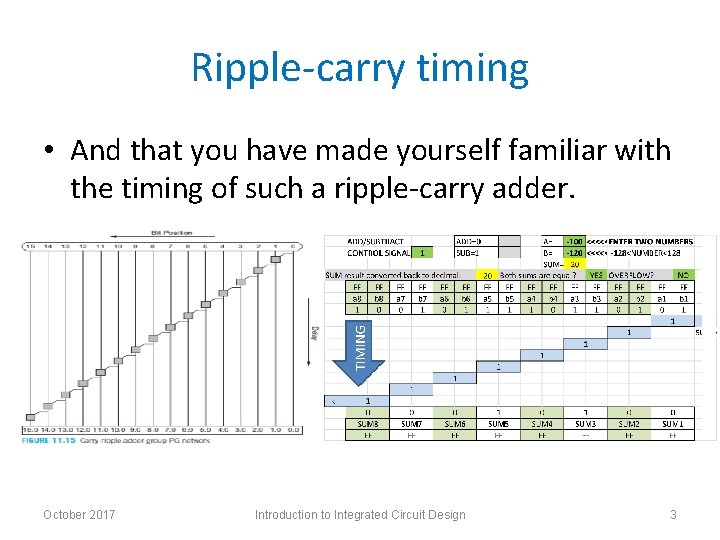
Ripple-carry timing • And that you have made yourself familiar with the timing of such a ripple-carry adder. October 2017 Introduction to Integrated Circuit Design 3

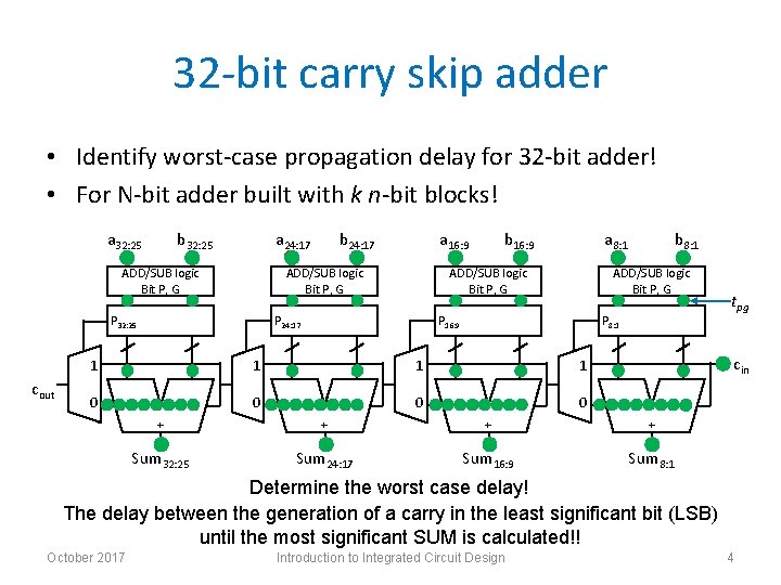
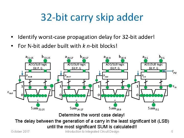
32 -bit carry skip adder • Identify worst-case propagation delay for 32 -bit adder! • For N-bit adder built with k n-bit blocks! a 32: 25 b 32: 25 a 24: 17 ADD/SUB logic Bit P, G a 16: 9 ADD/SUB logic Bit P, G P 32: 25 cout b 24: 17 b 16: 9 a 8: 1 ADD/SUB logic Bit P, G P 24: 17 b 8: 1 ADD/SUB logic Bit P, G P 16: 9 P 8: 1 1 1 0 0 tpg cin + + Sum 32: 25 Sum 24: 17 Sum 16: 9 Sum 8: 1 Determine the worst case delay! The delay between the generation of a carry in the least significant bit (LSB) until the most significant SUM is calculated!! October 2017 Introduction to Integrated Circuit Design 4

32 -bit carry skip adder • Identify worst-case propagation delay for 32 -bit adder! • For N-bit adder built with k n-bit blocks! a 32: 25 b 32: 25 a 24: 17 ADD/SUB logic Bit P, G a 16: 9 ADD/SUB logic Bit P, G P 32: 25 cout b 24: 17 b 16: 9 a 8: 1 ADD/SUB logic Bit P, G P 24: 17 b 8: 1 ADD/SUB logic Bit P, G P 16: 9 P 8: 1 1 1 0 0 tpg cin + + Sum 32: 25 Sum 24: 17 Sum 16: 9 Sum 8: 1 Determine the worst case delay! The delay between the generation of a carry in the least significant bit (LSB) until the most significant SUM is calculated!! October 2017 Introduction to Integrated Circuit Design 5

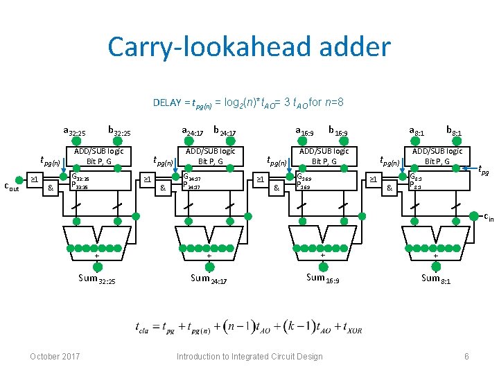
Carry-lookahead adder DELAY = tpg(n) = log 2(n)*t. AO= 3 t. AO for n=8 a 32: 25 tpg(n) cout ≥ 1 & b 32: 25 a 24: 17 b 24: 17 ADD/SUB logic Bit P, G G 32: 25 P 32: 25 tpg(n) ≥ 1 & a 16: 9 ADD/SUB logic Bit P, G G 24: 17 P 24: 17 tpg(n) ≥ 1 & b 16: 9 a 8: 1 ADD/SUB logic Bit P, G G 16: 9 P 16: 9 tpg(n) ≥ 1 & b 8: 1 ADD/SUB logic Bit P, G tpg G 8: 1 P 8: 1 cin + + Sum 32: 25 Sum 24: 17 Sum 16: 9 Sum 8: 1 October 2017 Introduction to Integrated Circuit Design 6

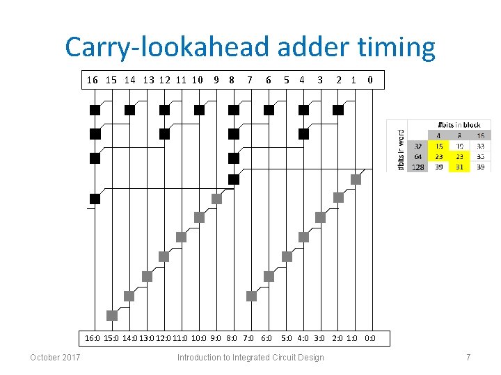
Carry-lookahead adder timing 16 15 14 13 12 11 10 9 8 7 6 16: 0 15: 0 14: 0 13: 0 12: 0 11: 0 10: 0 9: 0 8: 0 7: 0 6: 0 October 2017 5 4 3 2 1 0 5: 0 4: 0 3: 0 2: 0 1: 0 0: 0 Introduction to Integrated Circuit Design 7

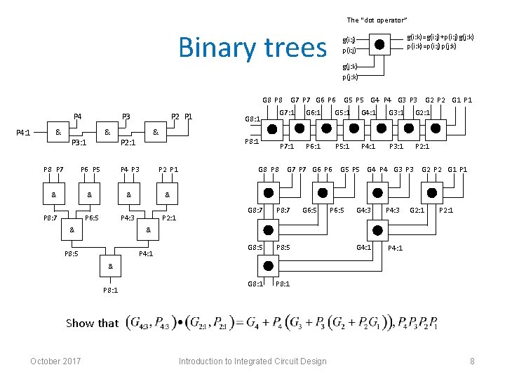
The “dot operator” Binary trees G 8 P 4 P 4: 1 & P 3: 1 P 2 P 1 & P 2: 1 P 8 P 7 P 6 P 5 P 4 P 3 P 2 P 1 & & P 4: 3 P 2: 1 P 8: 7 P 6: 5 G 8: 1 G 8 P 8 g(i: k)=g(i: j)+p(i: j)g(j: k) p(i: k)=p(i: j)p(j: k) g(i: j) p(i: j) g(j: k) p(j: k) G 7 P 7 G 6 P 6 G 5 P 5 G 4 P 4 G 3 P 3 G 2 P 2 G 1 P 1 G 7: 1 G 6: 1 G 5: 1 G 4: 1 G 3: 1 G 2: 1 P 7: 1 P 6: 1 P 5: 1 P 4: 1 P 3: 1 P 2: 1 G 7 P 7 G 6 P 6 G 8: 7 P 8: 7 G 8: 5 P 8: 5 G 8: 1 P 8: 1 G 6: 5 G 5 P 5 G 4 P 4 G 3 P 6: 5 G 4: 3 P 4: 3 G 2 P 2 G 1 P 1 G 2: 1 P 2: 1 & & P 8: 5 P 4: 1 G 4: 1 P 4: 1 & P 8: 1 Show that October 2017 Introduction to Integrated Circuit Design 8

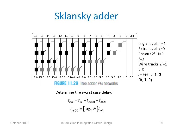
Sklansky adder 16 15 14 13 12 11 10 9 8 7 6 5 4 3 2 1←CIN 16: 0 15: 0 14: 0 13: 0 12: 0 11: 0 10: 0 9: 0 8: 0 7: 0 6: 0 5: 0 4: 0 3: 0 2: 0 1: 0 0: 0 Logic levels L=4 Extra levels l=0 Fanout 2 f+1=9 f=3 Wire tracks 2 t=1 t=0 l+f+t=L-1=3 (0, 3, 0) Determine the worst case delay! October 2017 Introduction to Integrated Circuit Design 9

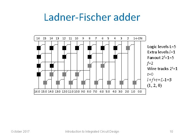
Ladner-Fischer adder 16 15 14 13 12 11 10 9 8 7 6 5 4 3 2 1←CIN Logic levels L=5 Extra levels l=1 Fanout 2 f+1=5 f=2 Wire tracks 2 t=1 t=0 l+f+t=L-1=3 (1, 2, 0) 16: 0 15: 0 14: 0 13: 0 12: 0 11: 0 10: 0 9: 0 8: 0 7: 0 6: 0 5: 0 4: 0 3: 0 2: 0 1: 0 0: 0 October 2017 Introduction to Integrated Circuit Design 10

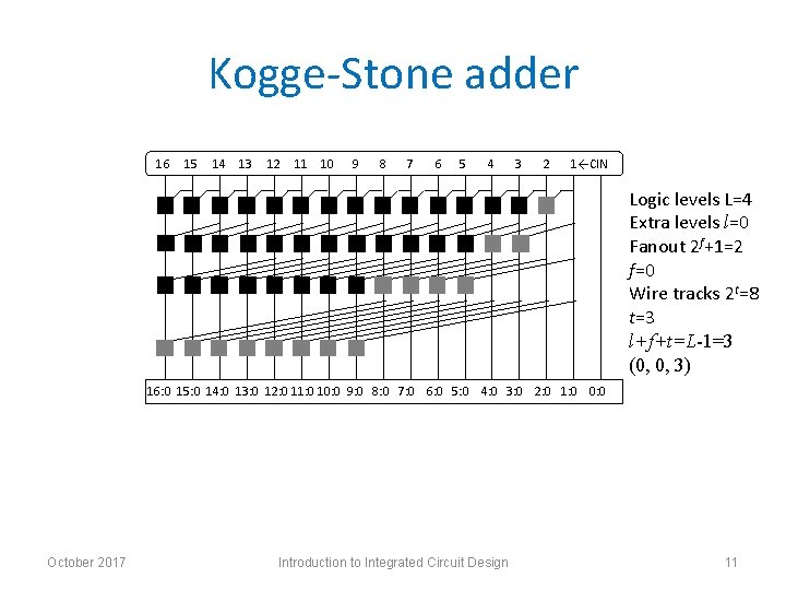
Kogge-Stone adder 16 15 14 13 12 11 10 9 8 7 6 5 4 3 2 1←CIN Logic levels L=4 Extra levels l=0 Fanout 2 f+1=2 f=0 Wire tracks 2 t=8 t=3 l+f+t=L-1=3 (0, 0, 3) 16: 0 15: 0 14: 0 13: 0 12: 0 11: 0 10: 0 9: 0 8: 0 7: 0 6: 0 5: 0 4: 0 3: 0 2: 0 1: 0 0: 0 October 2017 Introduction to Integrated Circuit Design 11

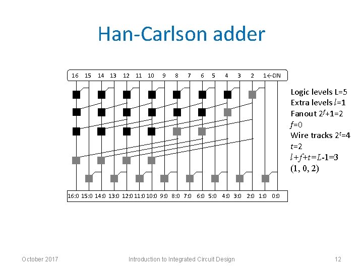
Han-Carlson adder 16 15 14 13 12 11 10 9 8 7 6 5 4 3 2 1←CIN Logic levels L=5 Extra levels l=1 Fanout 2 f+1=2 f=0 Wire tracks 2 t=4 t=2 l+f+t=L-1=3 (1, 0, 2) 16: 0 15: 0 14: 0 13: 0 12: 0 11: 0 10: 0 9: 0 8: 0 7: 0 6: 0 5: 0 4: 0 3: 0 2: 0 1: 0 0: 0 October 2017 Introduction to Integrated Circuit Design 12

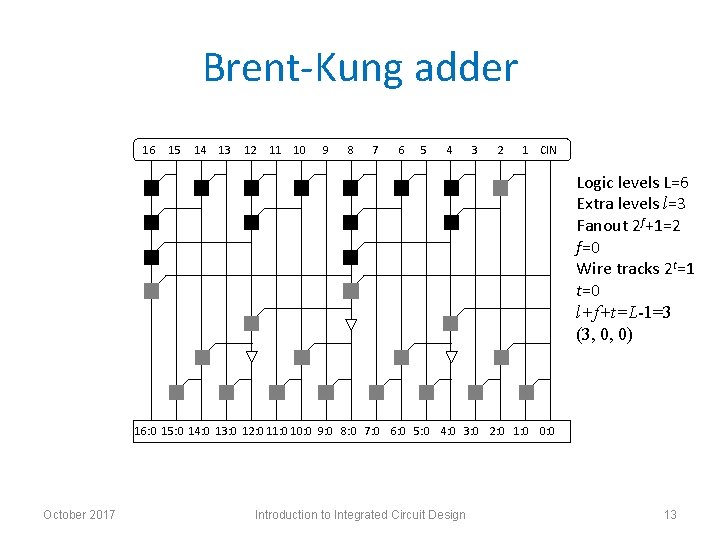
Brent-Kung adder 16 15 14 13 12 11 10 9 8 7 6 5 4 3 2 1 CIN Logic levels L=6 Extra levels l=3 Fanout 2 f+1=2 f=0 Wire tracks 2 t=1 t=0 l+f+t=L-1=3 (3, 0, 0) 16: 0 15: 0 14: 0 13: 0 12: 0 11: 0 10: 0 9: 0 8: 0 7: 0 6: 0 5: 0 4: 0 3: 0 2: 0 1: 0 0: 0 October 2017 Introduction to Integrated Circuit Design 13

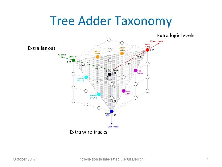
Tree Adder Taxonomy Extra logic levels Extra fanout Extra wire tracks October 2017 Introduction to Integrated Circuit Design 14

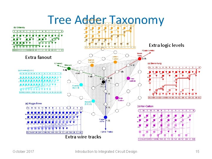
Tree Adder Taxonomy Extra logic levels Extra fanout Extra wire tracks October 2017 Introduction to Integrated Circuit Design 15

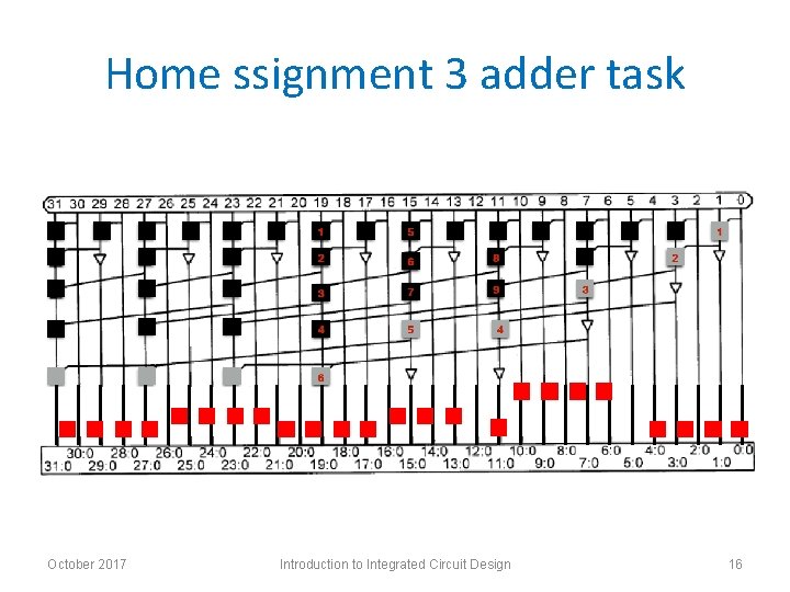
Home ssignment 3 adder task October 2017 Introduction to Integrated Circuit Design 16

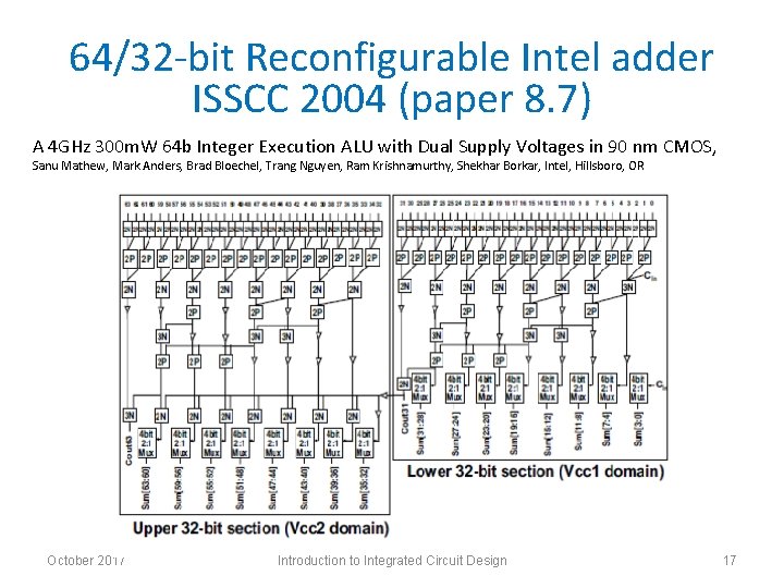
64/32 -bit Reconfigurable Intel adder ISSCC 2004 (paper 8. 7) A 4 GHz 300 m. W 64 b Integer Execution ALU with Dual Supply Voltages in 90 nm CMOS, Sanu Mathew, Mark Anders, Brad Bloechel, Trang Nguyen, Ram Krishnamurthy, Shekhar Borkar, Intel, Hillsboro, OR October 2017 Introduction to Integrated Circuit Design 17

Summary After this interactive lecture you will know about • Carry-skip adders, carry-lookahead adders and prefix-tree adders like Sklansky adders, etc. • You can identify the worst-case propagation delay for N-bit carry-skip and carry-lookahead adders built from k n-bit blocks • You can identify the worst-case delay for prefix-tree adders like Sklansky adders. • Using the same principles, you should also be able to do so for the unknown prefix-tree adder in home assignment 3. • Using the same principles, you should also be able to do so in the written exam for some of the other prefix-tree adders like Brent-Kung and Ladner-Fischer. October 2017 Introduction to Integrated Circuit Design 18

Q&A October 2017 Introduction to Integrated Circuit Design 19