21 st International Workshop on DEPFET Detectors and
![Power overview (worst case) Supply AVDD VREF_IN VAMP_LO DVDD VDMC_CORE VDMC_IO Total Voltg. [V] Power overview (worst case) Supply AVDD VREF_IN VAMP_LO DVDD VDMC_CORE VDMC_IO Total Voltg. [V]](https://slidetodoc.com/presentation_image_h2/5d38dac205622486dc264e80d7ab1986/image-24.jpg)
![Other voltages: Generate on MIC voltage range Net V_low [V] -50 V_high [V] 0 Other voltages: Generate on MIC voltage range Net V_low [V] -50 V_high [V] 0](https://slidetodoc.com/presentation_image_h2/5d38dac205622486dc264e80d7ab1986/image-25.jpg)
- Slides: 28

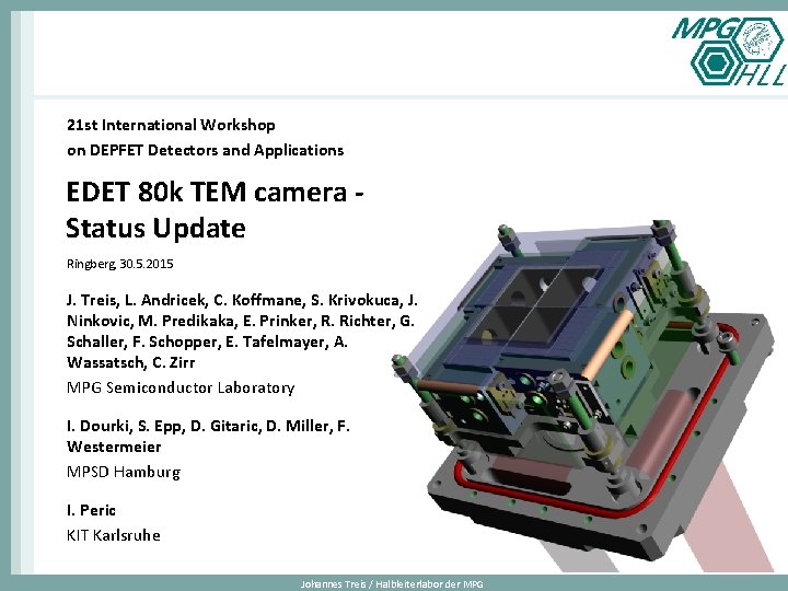
21 st International Workshop on DEPFET Detectors and Applications EDET 80 k TEM camera Status Update Ringberg, 30. 5. 2015 J. Treis, L. Andricek, C. Koffmane, S. Krivokuca, J. Ninkovic, M. Predikaka, E. Prinker, R. Richter, G. Schaller, F. Schopper, E. Tafelmayer, A. Wassatsch, C. Zirr MPG Semiconductor Laboratory I. Dourki, S. Epp, D. Gitaric, D. Miller, F. Westermeier MPSD Hamburg I. Peric KIT Karlsruhe Johannes Treis / Halbleiterlabor der MPG

Contents • Introduction to the instrument • DLSP • Power issues • MIC design • Roadmap • Summary & Outlook Johannes Treis / Halbleiterlabor der MPG

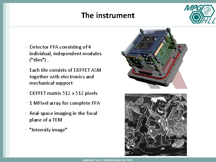
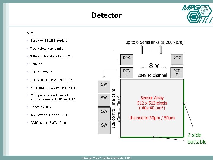
The instrument • Detector FPA consisting of 4 individual, independent modules ("tiles"). • Each tile consists of DEPFET ASM together with electronics and mechanical support • DEPFET matrix 512 pixels • 1 MPixel array for complete FPA • Real-space imaging in the focal plane of a TEM • "Intensity image" Johannes Treis / Halbleiterlabor der MPG

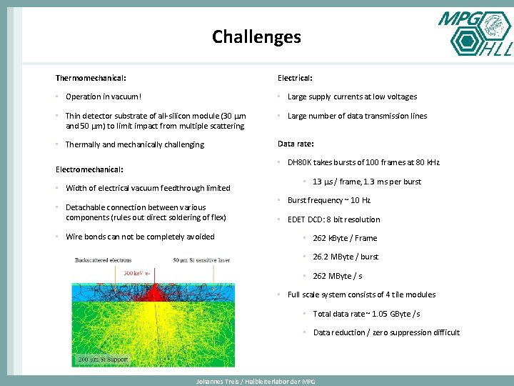
Challenges Thermomechanical: Electrical: • Operation in vacuum! • Large supply currents at low voltages • Thin detector substrate of all-silicon module (30 mm and 50 mm) to limit impact from multiple scattering • Large number of data transmission lines • Thermally and mechanically challenging Data rate: • DH 80 K takes bursts of 100 frames at 80 k. Hz Electromechanical: • Width of electrical vacuum feedthrough limited • Detachable connection between various components (rules out direct soldering of flex) • Wire bonds can not be completely avoided • 13 ms / frame, 1. 3 ms per burst • Burst frequency ~ 10 Hz • EDET DCD: 8 bit resolution • 262 k. Byte / Frame • 26. 2 MByte / burst • 262 MByte / s • Full scale system consists of 4 tile modules • Total data rate ~ 1. 05 GByte /s • Data reduction / zero suppression difficult Johannes Treis / Halbleiterlabor der MPG

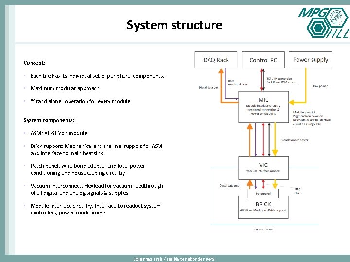
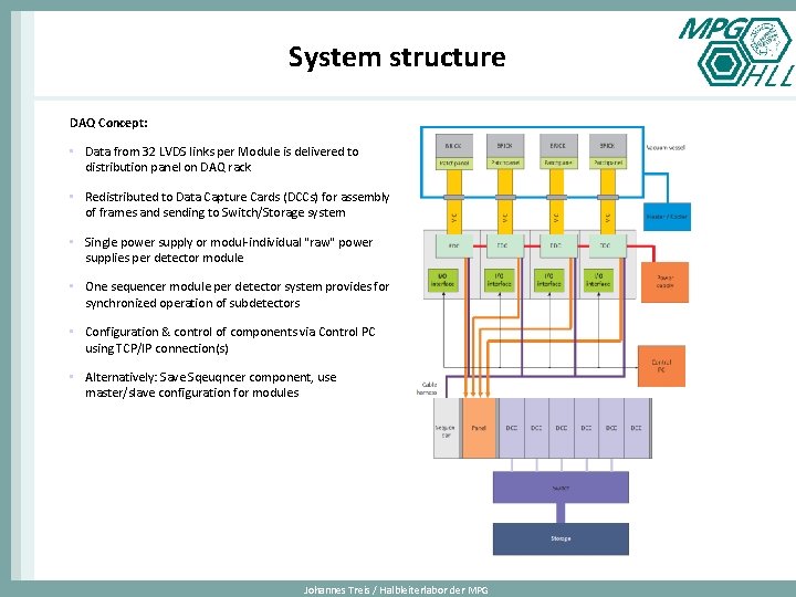
System structure Concept: • Each tile has its individual set of peripheral components: • Maximum modular approach • "Stand alone" operation for every module System components: • ASM: All-Silicon module • Brick support: Mechanical and thermal support for ASM and interface to main heatsink • Patch panel: Wire bond adapter and local power conditioning and housekeeping circuitry • Vacuum interconnect: Flexlead for vacuum feedthrough of all digital and analog signals & supplies • Module interface circuitry: Interface to readout system controllers, power conditioning Johannes Treis / Halbleiterlabor der MPG

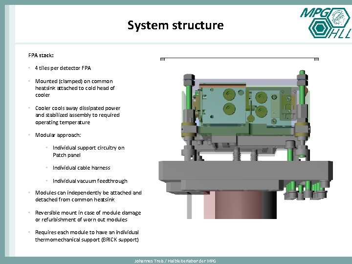
System structure FPA stack: • 4 tiles per detector FPA • Mounted (clamped) on common heatsink attached to cold head of cooler • Cooler cools away dissipated power and stabilized assembly to required operating temperature • Modular approach: • Individual support circuitry on Patch panel • Individual cable harness • Individual vacuum feedthrough • Modules can independently be attached and detached from common heatsink • Reversible mount in case of module damage or refurbishment of worn out modules • Requires each module to have an individual thermomechanical support (BRICK support) Johannes Treis / Halbleiterlabor der MPG

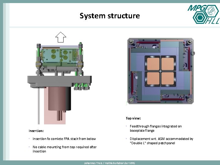
System structure Top view: • Feedthrough flanges integrated on baseplate flange Insertion: • Insertion fo comlete FPA stack from below • No cable mounting from top required after insertion • Displacement wrt. ASM accommodated by "Double L" shaped patchpanel Johannes Treis / Halbleiterlabor der MPG

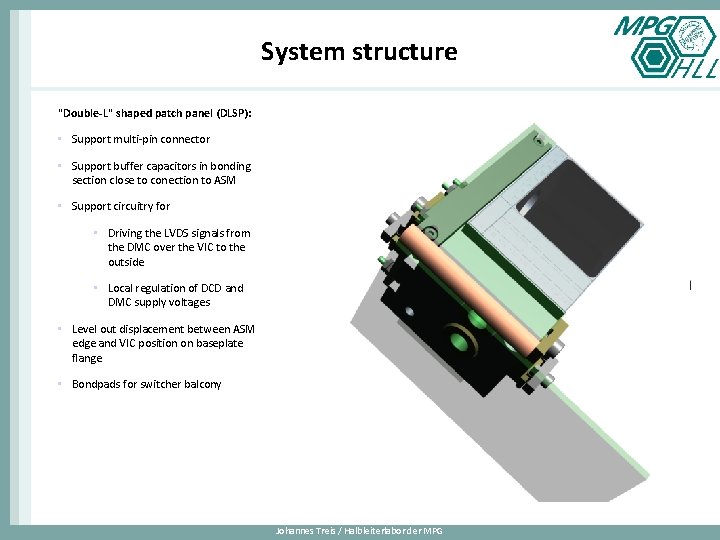
System structure "Double-L" shaped patch panel (DLSP): • Support multi-pin connector • Support buffer capacitors in bonding section close to conection to ASM • Support circuitry for • Driving the LVDS signals from the DMC over the VIC to the outside • Local regulation of DCD and DMC supply voltages • Level out displacement between ASM edge and VIC position on baseplate flange • Bondpads for switcher balcony Johannes Treis / Halbleiterlabor der MPG

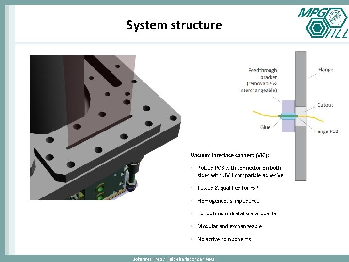
System structure Vacuum interface connect (VIC): • Potted PCB with connector on both sides with UVH compatible adhesive • Tested & qualified for FSP • Homogeneous impedance • For optimum digital signal quality • Modular and exchangeable • No active components Johannes Treis / Halbleiterlabor der MPG

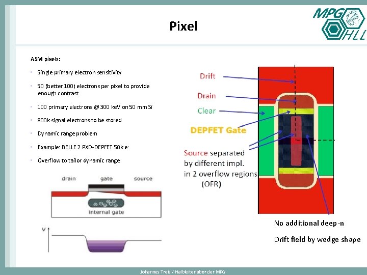
Pixel ASM pixels: • Single primary electron sensitivity • 50 (better 100) electrons per pixel to provide enough contrast • 100 primary electrons @ 300 ke. V on 50 mm Si • 800 k signal electrons to be stored • Dynamic range problem • Example: BELLE 2 PXD-DEPFET 50 k e • Overflow to tailor dynamic range No additional deep-n Drift field by wedge shape Johannes Treis / Halbleiterlabor der MPG

Detector ASM: • Based on BELLE 2 module • Technology very similar … • 2 Poly, 3 Metal (including Cu) • Thinned • 2 side buttable • Accessible from 2 other sides • Beneficial for system integration • Configuration and control structure similar to PXD-9 ASM • Specific ASICS • Application-specific DCD • DMC as data Buffer Chip Johannes Treis / Halbleiterlabor der MPG

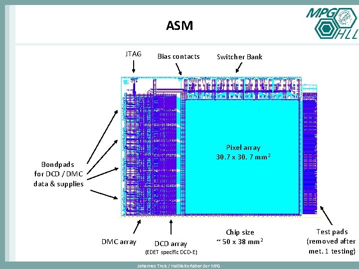
ASM JTAG Bias contacts Switcher Bank Pixel array 30. 7 x 30. 7 mm 2 Bondpads for DCD / DMC data & supplies DMC array DCD array Chip size ~ 50 x 38 mm 2 (EDET specific DCD-E) Johannes Treis / Halbleiterlabor der MPG Test pads (removed after met. 1 testing)

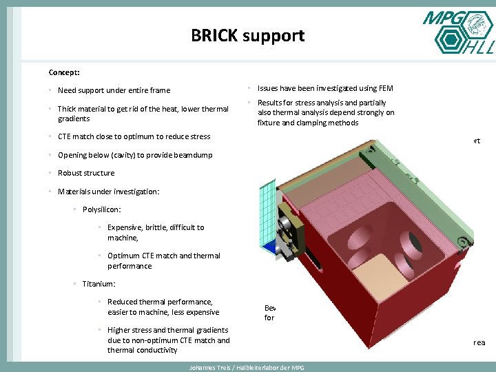
BRICK support Concept: • Need support under entire frame • Issues have been investigated using FEM • Thick material to get rid of the heat, lower thermal gradients • Results for stress analysis and partially also thermal analysis depend strongly on fixture and clamping methods • CTE match close to optimum to reduce stress ASM glued to Brick support • Opening below (cavity) to provide beamdump • Robust structure • Materials under investigation: • Polysilicon: • Expensive, brittle, difficult to machine, • Optimum CTE match and thermal performance • Titanium: • Reduced thermal performance, easier to machine, less expensive Bevelled aproach for beam dump • Higher stress and thermal gradients due to non-optimum CTE match and thermal conductivity Johannes Treis / Halbleiterlabor der MPG Thermal support over full backside area equal reference temperature of 0°

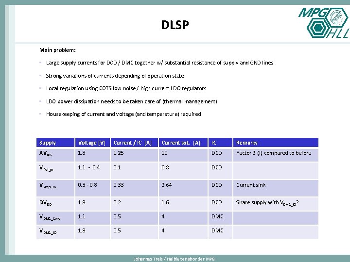
DLSP Main problem: • Large supply currents for DCD / DMC together w/ substantial resistance of supply and GND lines • Strong variations of currents depending of operation state • Local regulation using COTS low noise / high current LDO regulators • LDO power dissipation needs to be taken care of (thermal management) • Housekeeping of current and voltage (and temperature) required Supply Voltage [V] Current / IC [A] Current tot. [A] IC Remarks AVDD 1. 8 1. 25 10 DCD Factor 2 (!) compared to before VRef_in 1. 1 - 0. 4 0. 1 0. 8 DCD VAmp_Lo 0. 3 - 0. 8 0. 33 2. 64 DCD Current sink DVDD 1. 8 0. 2 1. 6 DCD Share supply with VDMC_IO? VDMC_Core 1. 1 0. 5 4 DMC VDMC_IO 1. 8 0. 5 4 DMC Johannes Treis / Halbleiterlabor der MPG

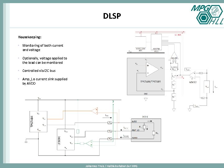
DLSP Housekeeping: • Monitoring of both current and voltage • Optionally, voltage applied to the load can be monitored • Controlled via I 2 C bus • Amp_Lo current sink supplied by AVDD Johannes Treis / Halbleiterlabor der MPG

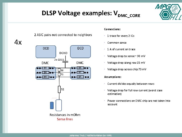
DLSP Voltage examples: VDMC_CORE Connections: • 1 trace for every 2 ICs • Common sense • 1 A of current on trace • Voltage drop to sense ~ 98 m. V • Voltage drop along row 15 m. V • Voltage drop across chip 73 m. V Assumptions: • Current divides equally between rows • Voltage drop for full row current (worst case estimation) • Power connections on DMC chip are not taken into account Johannes Treis / Halbleiterlabor der MPG

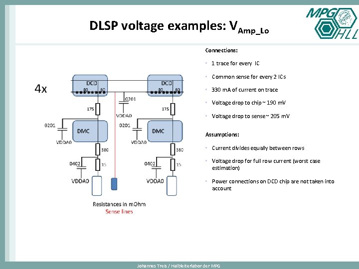
DLSP voltage examples: VAmp_Lo Connections: • 1 trace for every IC • Common sense for every 2 ICs • 330 m. A of current on trace • Voltage drop to chip ~ 190 m. V • Voltage drop to sense ~ 205 m. V Assumptions: • Current divides equally between rows • Voltage drop for full row current (worst case estimation) • Power connections on DCD chip are not taken into account Johannes Treis / Halbleiterlabor der MPG

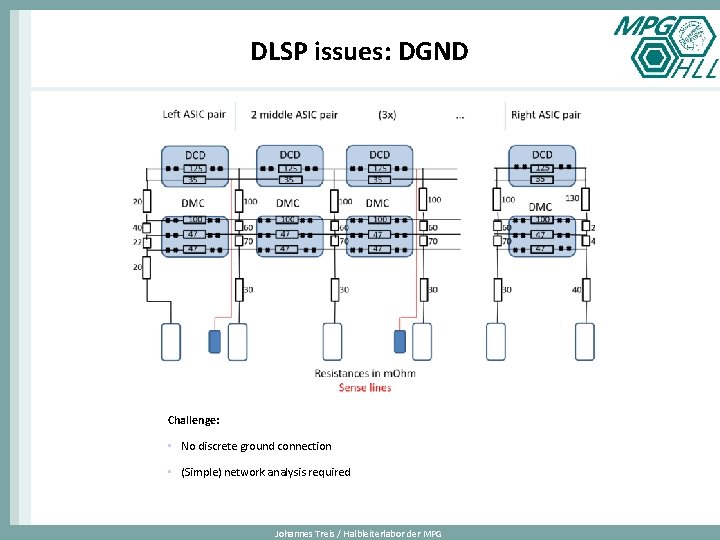
DLSP issues: DGND Challenge: • No discrete ground connection • (Simple) network analysis required Johannes Treis / Halbleiterlabor der MPG

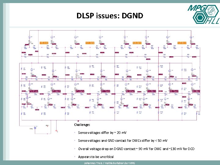
DLSP issues: DGND Challenge: • Sense voltages differ by ~ 20 m. V • Sense voltages and GND contact for DMCs differ by < 50 m. V • Overall voltage drop on DGND contact ~ 90 m. V for DMC and ~130 m. V for DCD • Appears to be uncritical Johannes Treis / Halbleiterlabor der MPG

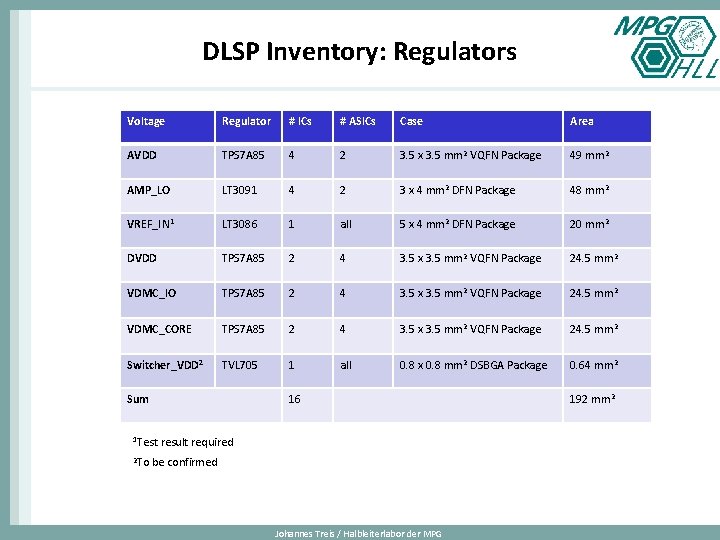
DLSP Inventory: Regulators Voltage Regulator # ICs # ASICs Case Area AVDD TPS 7 A 85 4 2 3. 5 x 3. 5 mm 2 VQFN Package 49 mm 2 AMP_LO LT 3091 4 2 3 x 4 mm 2 DFN Package 48 mm 2 VREF_IN 1 LT 3086 1 all 5 x 4 mm 2 DFN Package 20 mm 2 DVDD TPS 7 A 85 2 4 3. 5 x 3. 5 mm 2 VQFN Package 24. 5 mm 2 VDMC_IO TPS 7 A 85 2 4 3. 5 x 3. 5 mm 2 VQFN Package 24. 5 mm 2 VDMC_CORE TPS 7 A 85 2 4 3. 5 x 3. 5 mm 2 VQFN Package 24. 5 mm 2 Switcher_VDD 2 TVL 705 1 all 0. 8 x 0. 8 mm 2 DSBGA Package 0. 64 mm 2 Sum 16 1 Test 2 To result required be confirmed Johannes Treis / Halbleiterlabor der MPG 192 mm 2

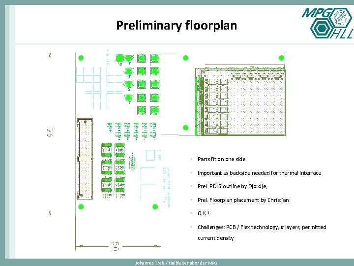
Preliminary floorplan • Parts fit on one side • Important as backside needed for thermal interface • Prel. PDLS outline by Djordje, • Prel. Floorplan placement by Christian • O. K. ! • Challenges: PCB / Flex technology, # layers, permitted current density Johannes Treis / Halbleiterlabor der MPG

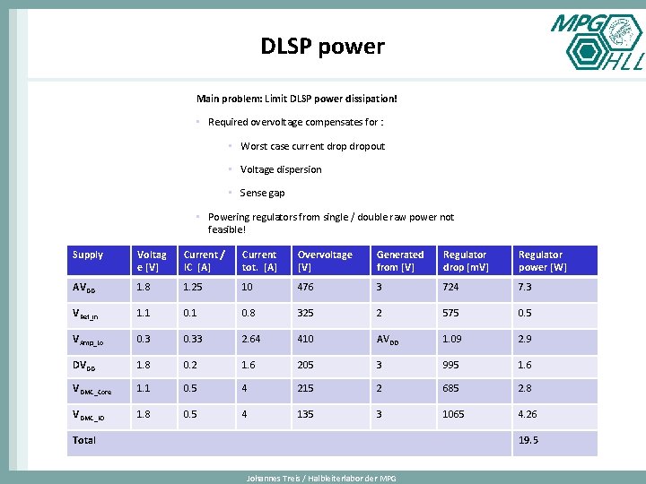
DLSP power Main problem: Limit DLSP power dissipation! • Required overvoltage compensates for : • Worst case current dropout • Voltage dispersion • Sense gap • Powering regulators from single / double raw power not feasible! Supply Voltag e [V] Current / IC [A] Current tot. [A] Overvoltage [V] Generated from [V] Regulator drop [m. V] Regulator power [W] AVDD 1. 8 1. 25 10 476 3 724 7. 3 VRef_in 1. 1 0. 8 325 2 575 0. 5 VAmp_Lo 0. 33 2. 64 410 AVDD 1. 09 2. 9 DVDD 1. 8 0. 2 1. 6 205 3 995 1. 6 VDMC_Core 1. 1 0. 5 4 215 2 685 2. 8 VDMC_IO 1. 8 0. 5 4 135 3 1065 4. 26 Total 19. 5 Johannes Treis / Halbleiterlabor der MPG

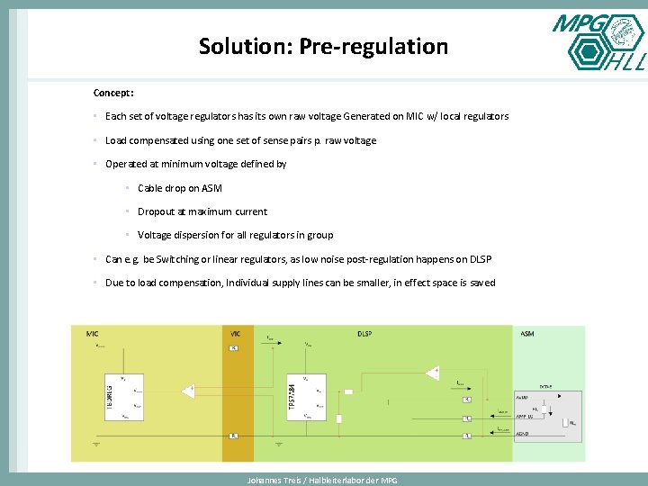
Solution: Pre-regulation Concept: • Each set of voltage regulators has its own raw voltage Generated on MIC w/ local regulators • Load compensated using one set of sense pairs p. raw voltage • Operated at minimum voltage defined by • Cable drop on ASM • Dropout at maximum current • Voltage dispersion for all regulators in group • Can e. g. be Switching or linear regulators, as low noise post-regulation happens on DLSP • Due to load compensation, Individual supply lines can be smaller, in effect space is saved Johannes Treis / Halbleiterlabor der MPG
![Power overview worst case Supply AVDD VREFIN VAMPLO DVDD VDMCCORE VDMCIO Total Voltg V Power overview (worst case) Supply AVDD VREF_IN VAMP_LO DVDD VDMC_CORE VDMC_IO Total Voltg. [V]](https://slidetodoc.com/presentation_image_h2/5d38dac205622486dc264e80d7ab1986/image-24.jpg)
Power overview (worst case) Supply AVDD VREF_IN VAMP_LO DVDD VDMC_CORE VDMC_IO Total Voltg. [V] 1. 8 0. 4 0. 8 1. 1 1. 8 ASM losses [m. V] Sense GND 290 220 210 205 90 100 120 290 140 150 OVC [m. V] n/a n/a 40 40 VD [m. V] 25 25 30 30 CNT [m. V] 100 50 100 100 VOut [V] 2. 45 0. 7 0. 2 2. 15 1. 5 2. 2 # Reg's I / Reg [A] VDO [m. V] VIn [V] P [W] Min Max 2 4 270 2. 75 2. 2 3 4 2 140 2. 6 1. 1 1. 2 1 0. 8 220 1. 4 0. 55 0. 6 4 0. 2 120 1. 4 0. 55 0. 6 2 1. 4 450 1. 8 2. 8 3. 1 4 0. 7 320 1. 8 2. 8 3. 1 2 0. 8 70 2. 25 0. 16 0. 32 4 0. 4 30 2. 2 0. 1 0. 25 2 2 140 1. 65 0. 6 1 4 1 70 1. 6 0. 4 0. 8 2 2 140 2. 35 0. 6 1 4 1 70 2. 3 0. 4 0. 8 light blue 7 9 dark blue 5. 4 6. 8 Johannes Treis / Halbleiterlabor der MPG
![Other voltages Generate on MIC voltage range Net Vlow V 50 Vhigh V 0 Other voltages: Generate on MIC voltage range Net V_low [V] -50 V_high [V] 0](https://slidetodoc.com/presentation_image_h2/5d38dac205622486dc264e80d7ab1986/image-25.jpg)
Other voltages: Generate on MIC voltage range Net V_low [V] -50 V_high [V] 0 nominal voltage [V] -30 current [m. A] 0, 1 reference net source 1 DEPFET_BP 2 DEPFET_Bulk 0 20 10 0, 1 source 3 DEPFET_CLG -20 5 0 10 source 4 DEPFET_Drift -15 0 -5 1 source 5 DEPFET_Guard -15 0 -5 1 source 6 DEPFET_Source 0 8 6 1000 AGND 7 SW_Cl_Off 0 20 3 50 source 8 SW_Cl_On 0 20 18 50 source 9 SW_G_Off 0 10 3 50 source 10 SW_G_On -20 3 -2, 5 50 source 11 SW_VREF -25 0 -6, 2 50 source 12 SW_Substrate (current sink) -25 0 -8 50 source Benefit from FSP development – use similar circuits? This time outside vacuum! Johannes Treis / Halbleiterlabor der MPG

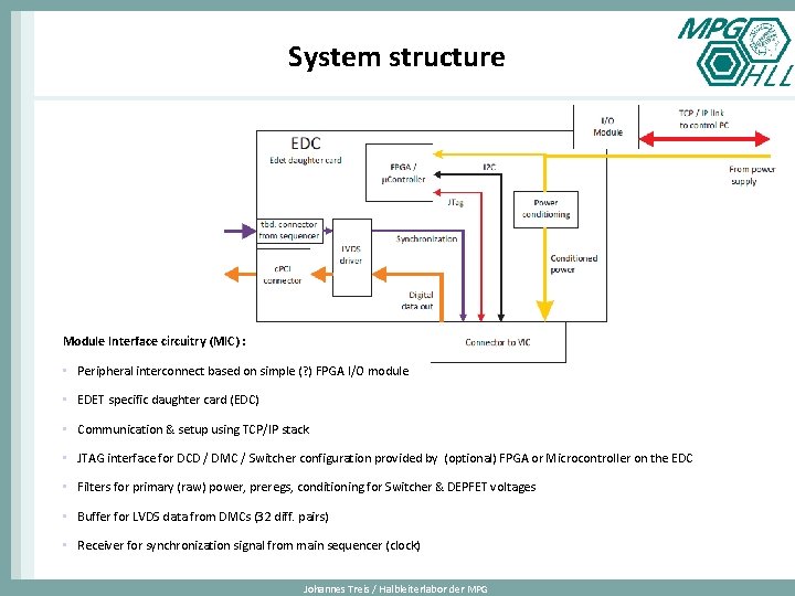
System structure Module Interface circuitry (MIC) : • Peripheral interconnect based on simple (? ) FPGA I/O module • EDET specific daughter card (EDC) • Communication & setup using TCP/IP stack • JTAG interface for DCD / DMC / Switcher configuration provided by (optional) FPGA or Microcontroller on the EDC • Filters for primary (raw) power, preregs, conditioning for Switcher & DEPFET voltages • Buffer for LVDS data from DMCs (32 diff. pairs) • Receiver for synchronization signal from main sequencer (clock) Johannes Treis / Halbleiterlabor der MPG

System structure DAQ Concept: • Data from 32 LVDS links per Module is delivered to distribution panel on DAQ rack • Redistributed to Data Capture Cards (DCCs) for assembly of frames and sending to Switch/Storage system • Single power supply or modul-individual "raw" power supplies per detector module • One sequencer module per detector system provides for synchronized operation of subdetectors • Configuration & control of components via Control PC using TCP/IP connection(s) • Alternatively: Save Sqeuqncer component, use master/slave configuration for modules Johannes Treis / Halbleiterlabor der MPG

Summary & Outlook Status: • ASMs produced • First detector measurements on small devices start soon • DCD-E available and partially qualified • DMC submission on critical path • DLSP prototyping successful • Roadmap for DLSP / MIC development Open questions: • Use Laser annealing for TID compensation? • Prereg concept (switching regulators? ) • DLSP techology Johannes Treis / Halbleiterlabor der MPG