Xray radiation damage of silicon strip detectors Piotr

- Slides: 24

X-ray radiation damage of silicon strip detectors Piotr Wiącek, Władysław Dąbrowski AGH University of Science and Technology Faculty of Physics and Applied Computer Science, Kraków, Poland Jagiellonian Symposium 2015 7 -12/06/2015

Outline • Radiation damage in silicon detector – short overview • Ionisation damage effects in a silicon strip detector for powder diffraction • Ionisation damage effects in a silicon pad detector for high resolution spectroscopy • Investigation of the dose rate effect • Summary

Radiation damage in silicon detectors Displacement damage by charged particles and neutrons – Creation of defects in the lattice – Some defects form localised electronic states, which behave like deep level depends in the energy bandgap – Deep levels act as generation-recombination centres and contribute to the bulk leakage current – Deep levels contribute to the effective doping of silicon and change the resistivity – In silicon most of the defects form acceptor-like deep levels – After sufficiently high fluence the low-doped n-type silicon (used commonly for silicon strip and pixel detectors) becomes p-type Displacement damage effects in silicon detectors for the LHC experiments have been extensively studied and are quite well understood.

Radiation damage in silicon detectors Ionisation damage by charged particles and by X and gamma radiation – Ionisation processes do not lead to any permanent defects in the silicon bulk – Ionisation processes lead to building-up positive charge in the insulator layers (Si. O 2/ Si 3 N 4) due to trapped holes – Additional surface states are generated in the Si-Si. O 2/Si 3 N 4 interface – Generation recombination processes at the surface states contribute to the surface leakage current • In silicon detectors for LHC experiments the ionisation effects have been mostly ignored as the effects due to displacement damages are dominant • Ionisation effects in Si. O 2 are the primary source of radiation damage in CMOS devices (electronics) • Radiation damage in silicon strip and silicon pixel detectors caused by X-ray has become recently an important research topic driven mainly by development of new detectors for applications at the intensive synchrotron sources

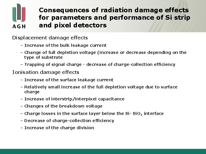
Consequences of radiation damage effects for parameters and performance of Si strip and pixel detectors Displacement damage effects – Increase of the bulk leakage current – Change of full depletion voltage (increase or decrease depending on the type of substrate – Trapping of signal charge - decrease of charge-collection efficiency Ionisation damage effects – Increase of the surface leakage current – Relatively small increase of the full depletion voltage due to surface charge – Increase of interstrip/interpixel capacitance – Changes of the breakdown voltage – Charge losses in the surface layer below the Si- Si. O 2 interface – Decrease of charge-collection efficiency – Increase of the charge division

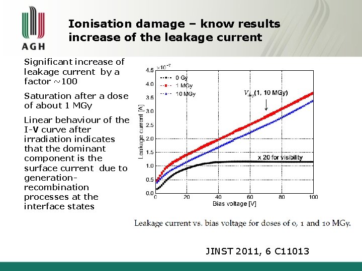
Ionisation damage – know results increase of the leakage current Significant increase of leakage current by a factor ~100 Saturation after a dose of about 1 MGy Linear behaviour of the I-V curve after irradiation indicates that the dominant component is the surface current due to generationrecombination processes at the interface states JINST 2011, 6 C 11013

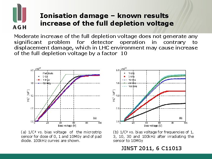
Ionisation damage – known results increase of the full depletion voltage Moderate increase of the full depletion voltage does not generate any significant problem for detector operation in contrary to displacement damage, which in LHC environment may cause increase of the full depletion voltage by a factor 10 (a) 1/C 2 vs. bias voltage of the microstrip sensor for dose of 0, 1 and 10 MGy and of pad diode. 100 k. Hz curves are shown. (b) 1/C 2 vs. bias voltage for frequencies of 1, 3, 10, 30 and 100 k. Hz after irradiating the sensor to 10 MGy JINST 2011, 6 C 11013

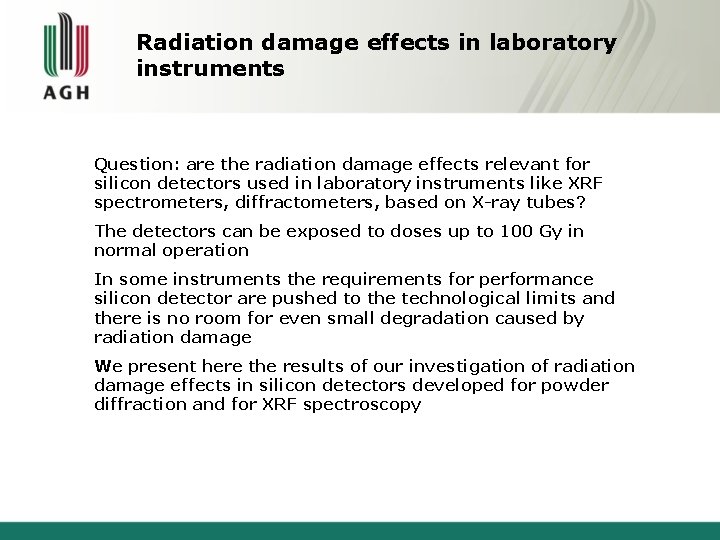
Radiation damage effects in laboratory instruments Question: are the radiation damage effects relevant for silicon detectors used in laboratory instruments like XRF spectrometers, diffractometers, based on X-ray tubes? The detectors can be exposed to doses up to 100 Gy in normal operation In some instruments the requirements for performance silicon detector are pushed to the technological limits and there is no room for even small degradation caused by radiation damage We present here the results of our investigation of radiation damage effects in silicon detectors developed for powder diffraction and for XRF spectroscopy

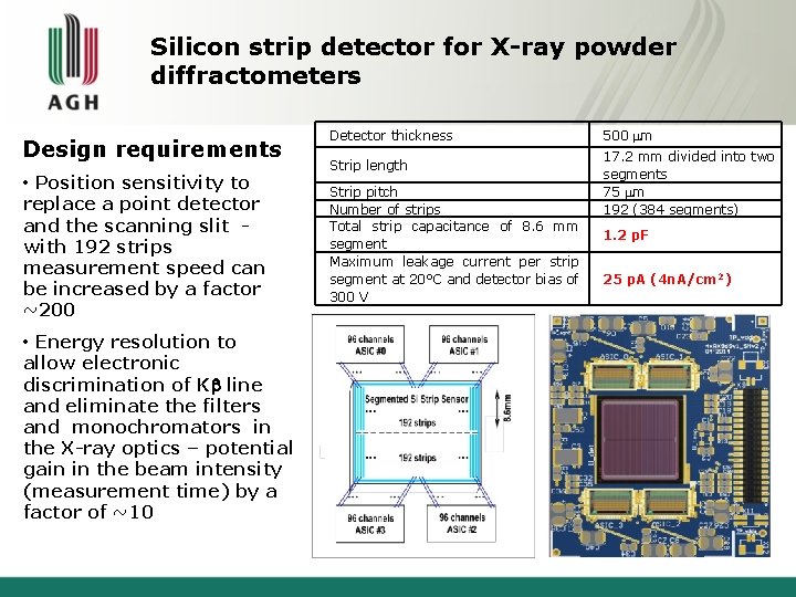
Silicon strip detector for X-ray powder diffractometers Design requirements • Position sensitivity to replace a point detector and the scanning slit with 192 strips measurement speed can be increased by a factor ~200 • Energy resolution to allow electronic discrimination of Kb line and eliminate the filters and monochromators in the X-ray optics – potential gain in the beam intensity (measurement time) by a factor of ~10 Detector thickness Strip length Strip pitch Number of strips Total strip capacitance of 8. 6 mm segment Maximum leakage current per strip segment at 20°C and detector bias of 300 V 500 mm 17. 2 mm divided into two segments 75 mm 192 (384 segments) 1. 2 p. F 25 p. A (4 n. A/cm 2)

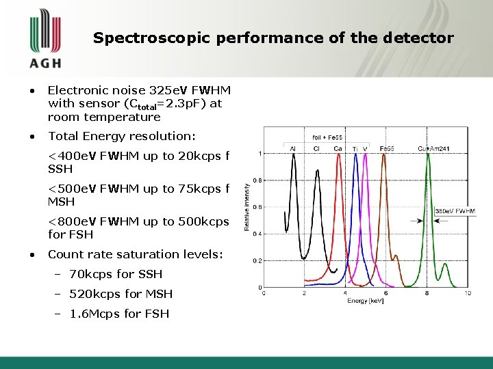
Spectroscopic performance of the detector • Electronic noise 325 e. V FWHM with sensor (Ctotal=2. 3 p. F) at room temperature • Total Energy resolution: <400 e. V FWHM up to 20 kcps for SSH <500 e. V FWHM up to 75 kcps for MSH <800 e. V FWHM up to 500 kcps for FSH • Count rate saturation levels: – 70 kcps for SSH – 520 kcps for MSH – 1. 6 Mcps for FSH

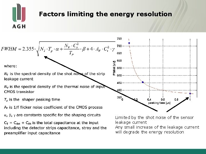
Factors limiting the energy resolution Limited by the shot noise of the sensor leakage current Any small increase of the leakage current will degrade the energy resolution

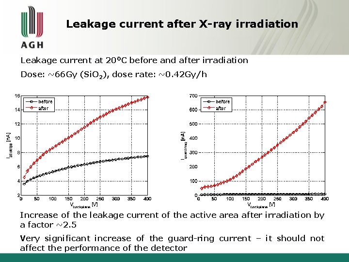
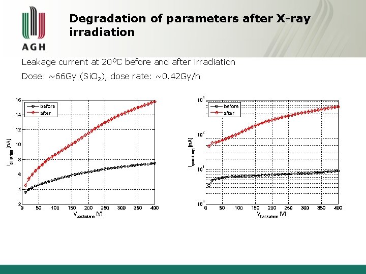
Leakage current after X-ray irradiation Leakage current at 20 OC before and after irradiation Dose: ~66 Gy (Si. O 2), dose rate: ~0. 42 Gy/h Increase of the leakage current of the active area after irradiation by a factor ~2. 5 Very significant increase of the guard-ring current – it should not affect the performance of the detector

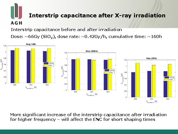
Interstrip capacitance after X-ray irradiation Interstrip capacitance before and after irradiation Dose: ~66 Gy (Si. O 2), dose rate: ~0. 42 Gy/h, cumulative time: ~160 h More significant increase of the interstrip capacitance after irradiation for higher frequency – will affect the ENC for short shaping times

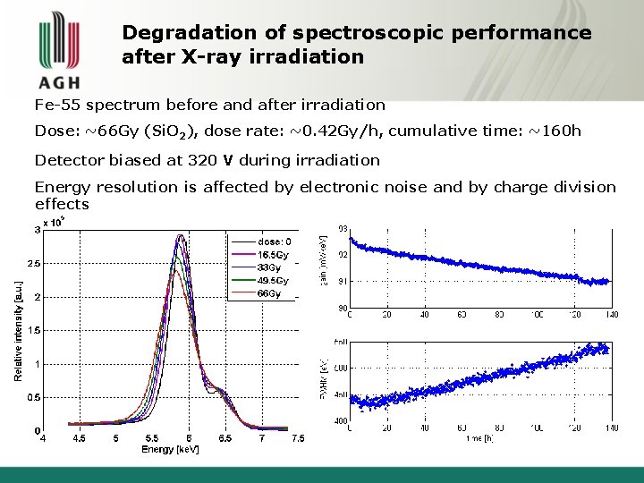
Degradation of spectroscopic performance after X-ray irradiation Fe-55 spectrum before and after irradiation Dose: ~66 Gy (Si. O 2), dose rate: ~0. 42 Gy/h, cumulative time: ~160 h Detector biased at 320 V during irradiation Energy resolution is affected by electronic noise and by charge division effects

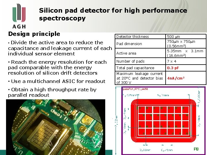
Silicon pad detector for high performance spectroscopy Design principle Detector thickness • Divide the active area to reduce the Pad dimension capacitance and leakage current of each individual sensor element • Reach the energy resolution for each pad comparable with the energy resolution of silicon drift detectors • Use a multichannel ASIC for readout • Obtain a high throughput rate by parallel readout Active area 500 mm 750 mm x 750 mm (0. 56 mm 2) 5. 35 mm x 3. 1 mm (16. 6 mm 2) Number of pads 7 x 4 Total pad capacitance 0. 3 p. F Maximum leakage current at 20°C and detector bias of 300 V 4 n. A/cm 2

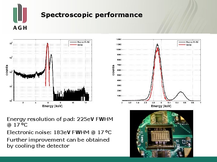
Spectroscopic performance Energy resolution of pad: 225 e. V FWHM @ 17 OC Electronic noise: 183 e. V FWHM @ 17 OC Further improvement can be obtained by cooling the detector

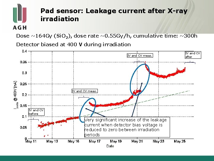
Pad sensor: Leakage current after X-ray irradiation Dose ~164 Gy (Si. O 2), dose rate ~0. 55 Gy/h, cumulative time: ~300 h Detector biased at 400 V during irradiation IV and CV meas. IV and CV before Very significant increase of the leakage current when detector bias voltage is reduced to zero between irradiation periods IV and CV after

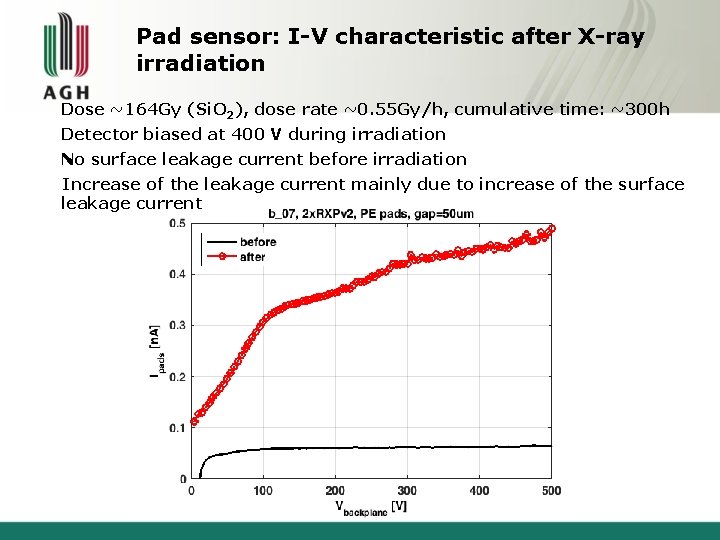
Pad sensor: I-V characteristic after X-ray irradiation Dose ~164 Gy (Si. O 2), dose rate ~0. 55 Gy/h, cumulative time: ~300 h Detector biased at 400 V during irradiation No surface leakage current before irradiation Increase of the leakage current mainly due to increase of the surface leakage current

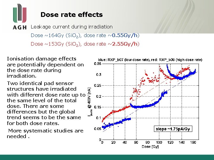
Dose rate effects Leakage current during irradiation Dose ~164 Gy (Si. O 2), dose rate ~0. 55 Gy/h) Dose ~153 Gy (Si. O 2), dose rate ~2. 55 Gy/h) Ionisation damage effects are potentially dependent on the dose rate during irradiation. Two identical pad sensor structures have irradiated with different dose rate up to the same level of the total dose. There are some differences but the global trend seems to be the same for both dose rates. More systematic studies are needed.

Summary Ionisation damage effects caused by soft X-rays in silicon strip and silicon pad detectors are observed starting from very low doses of a few Grays. The main effects which affect performance of the detector are: Øincrease of the surface leakage current Øincrease of the interstrip capacitance Øbuilding-up of the positive charge in the inter-strip (inter-pixel) surface layers, which affect charge division In high performance detectors employed in the laboratory instruments using X-ray tubes the ionisation damage effects by soft X-rays cannot be ignored More of detail studies in the low dose region is needed

Back up slides

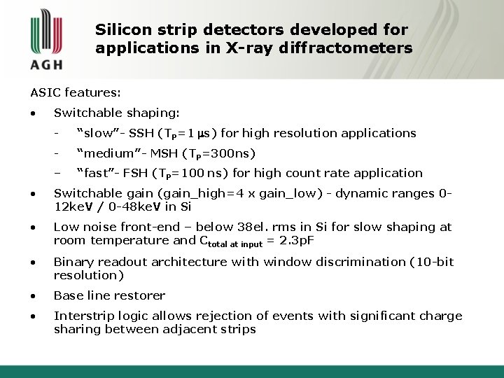
Silicon strip detectors developed for applications in X-ray diffractometers ASIC features: • Switchable shaping: - “slow”- SSH (TP=1 s) for high resolution applications - “medium”- MSH (TP=300 ns) – “fast”- FSH (TP=100 ns) for high count rate application • Switchable gain (gain_high=4 x gain_low) - dynamic ranges 012 ke. V / 0 -48 ke. V in Si • Low noise front-end – below 38 el. rms in Si for slow shaping at room temperature and Ctotal at input = 2. 3 p. F • Binary readout architecture with window discrimination (10 -bit resolution) • Base line restorer • Interstrip logic allows rejection of events with significant charge sharing between adjacent strips

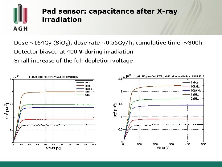
Pad sensor: capacitance after X-ray irradiation Dose ~164 Gy (Si. O 2), dose rate ~0. 55 Gy/h, cumulative time: ~300 h Detector biased at 400 V during irradiation Small increase of the full depletion voltage

Degradation of parameters after X-ray irradiation Leakage current at 20 OC before and after irradiation Dose: ~66 Gy (Si. O 2), dose rate: ~0. 42 Gy/h