Investigation of Charge Multiplication in Silicon Strip Detectors

- Slides: 29

Investigation of Charge Multiplication in Silicon Strip Detectors 20 th RD 50 Workshop 30. 05. - 01. 06. 2012 Lokman Altan, T. Barvich, F. Bögelspacher, W. de Boer, A. Dierlamm, K. -H. Hoffmann, R. Eber, A. Nürnberg, P. Steck Institut für Experimentelle Kernphysik KIT – University of the State of Baden-Wuerttemberg and National Research Center of the Helmholtz Association www. kit. edu

Overview Introduction Overview of sensor properties Qualification before and after irradiation IV/CV measurement Interstrip measurement Bias resistance and coupling capacitance Charge collection before and after irradiation CCE Signal to noise ratio Leakage current Summary 2 31. 05. 2012 Institut für Experimentelle Kernphysik, KIT

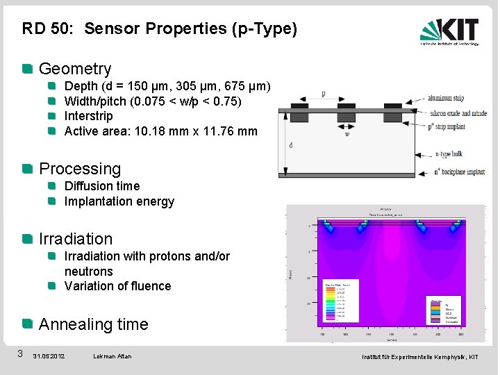
RD 50: Sensor Properties (p-Type) Geometry Depth (d = 150 µm, 305 µm, 675 µm) Width/pitch (0. 075 < w/p < 0. 75) Interstrip Active area: 10. 18 mm x 11. 76 mm Processing Diffusion time Implantation energy Irradiation with protons and/or neutrons Variation of fluence Annealing time 3 31. 05. 2012 Lokman Altan Institut für Experimentelle Kernphysik, KIT

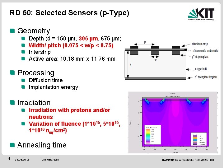
RD 50: Selected Sensors (p-Type) Geometry Depth (d = 150 µm, 305 µm, 675 µm) Width/ pitch (0. 075 < w/p < 0. 75) Interstrip Active area: 10. 18 mm x 11. 76 mm Processing Diffusion time Implantation energy Irradiation with protons and/or neutrons Variation of fluence (1*1015, 5*1015, 1*1016 neq/cm 2) Annealing time 4 31. 05. 2012 Lokman Altan Institut für Experimentelle Kernphysik, KIT

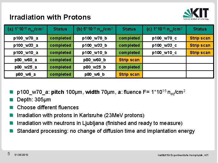
Irradiation with Protons (a) 1*1015 neq/cm 2 Status (b) 5*1015 neq/cm 2 Status (c) 1*1016 neq/cm 2 Status p 100_w 70_a completed p 100_w 70_b completed p 100_w 70_c Strip scan p 100_w 33_a completed p 100_w 33_b completed p 100_w 33_c Strip scan p 100_w 10_a completed p 100_w 10_b completed p 100_w 10_c Strip scan p 80_w 60_a completed p 80_w 60_b Strip scan p 80_w 25_a completed p 80_w 25_b completed p 80_w 6_a completed p 80_w 6_b Strip scan p 100_w 70_a: pitch 100µm, width 70µm, a: fluence F= 1*1015 neq/cm 2 Depth: 305µm Choose different fluences Irradiation with protons in Karlsruhe (23 Me. V protons) Irradiation with neutrons in Ljubljana (finished and ready to measure) Standard processing: no change of diffusion time and implantation energy 5 31. 05. 2012 Institut für Experimentelle Kernphysik, KIT

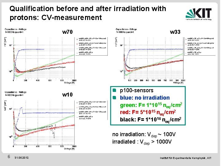
Qualification before and after irradiation with protons: CV-measurement w 70 w 10 w 33 p 100 -sensors blue: no irradiation green: F= 1*1015 neq/cm 2 red: F= 5*1015 neq/cm 2 black: F= 1*1016 neq/cm 2 no irradiation: Vdep ~ 100 V irradiated : Vdep > 1000 V 6 31. 05. 2012 Institut für Experimentelle Kernphysik, KIT

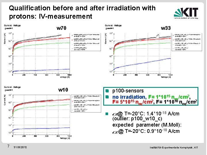
Qualification before and after irradiation with protons: IV-measurement w 70 w 10 w 33 p 100 -sensors no irradiation, F= 1*1015 neq/cm 2, F= 5*1015 neq/cm 2, F= 1*1016 neq/cm 2 @ T=-20°C: 1. 4*10 -18 A/cm (outlier: p 100_w 10_c) expected parameter (M. Moll): @ T=-20°C: 0. 9*10 -18 A/cm 7 31. 05. 2012 Institut für Experimentelle Kernphysik, KIT

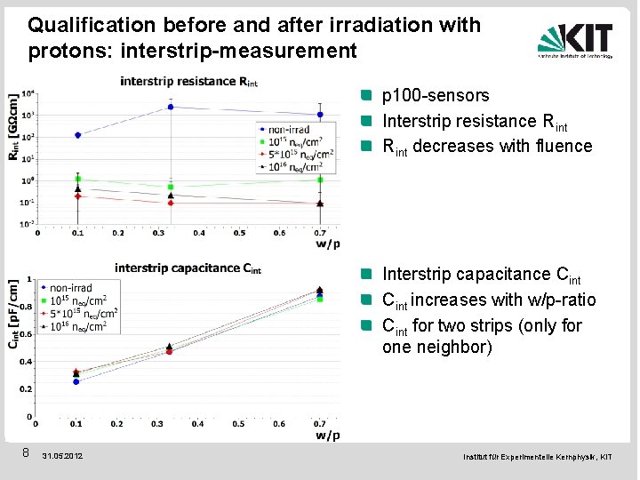
Qualification before and after irradiation with protons: interstrip-measurement p 100 -sensors Interstrip resistance Rint decreases with fluence Interstrip capacitance Cint increases with w/p-ratio Cint for two strips (only for one neighbor) 8 31. 05. 2012 Institut für Experimentelle Kernphysik, KIT

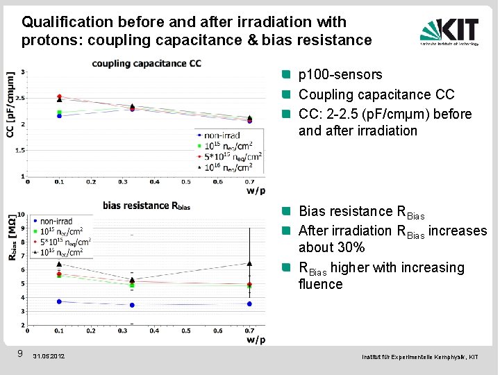
Qualification before and after irradiation with protons: coupling capacitance & bias resistance p 100 -sensors Coupling capacitance CC CC: 2 -2. 5 (p. F/cmµm) before and after irradiation Bias resistance RBias After irradiation RBias increases about 30% RBias higher with increasing fluence 9 31. 05. 2012 Institut für Experimentelle Kernphysik, KIT

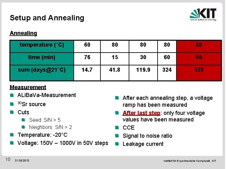
Setup and Annealing temperature (°C) 60 80 80 time (min) 76 15 30 60 60 sum (days@21°C) 14. 7 41. 8 119. 9 324 528 Measurement ALi. Ba. Va-Measurement 90 Sr source Cuts Seed: S/N > 5 Neighbors: S/N > 2 Temperature: -20°C Voltage: 150 V – 1000 V in 50 V steps 10 31. 05. 2012 After each annealing step, a voltage ramp has been measured After last step: only four voltage values have been measured CCE Signal to noise ratio Leakage current Institut für Experimentelle Kernphysik, KIT

Measurement Results Pitch = 100 µm 11 31. 05. 2012 Institut für Experimentelle Kernphysik, KIT

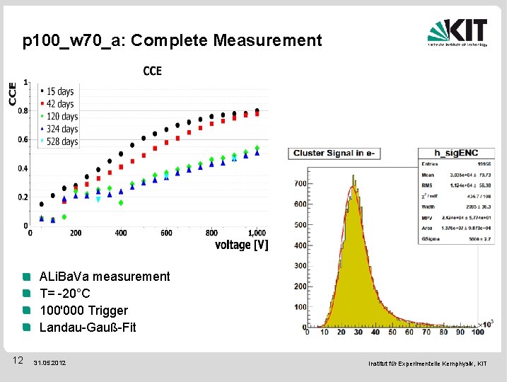
p 100_w 70_a: Complete Measurement ALi. Ba. Va measurement T= -20°C 100'000 Trigger Landau-Gauß-Fit 12 31. 05. 2012 Institut für Experimentelle Kernphysik, KIT

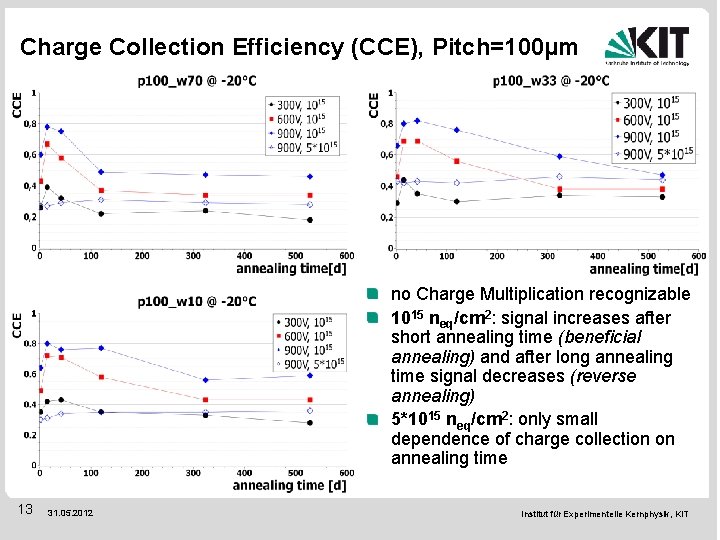
Charge Collection Efficiency (CCE), Pitch=100µm no Charge Multiplication recognizable 1015 neq/cm 2: signal increases after short annealing time (beneficial annealing) and after long annealing time signal decreases (reverse annealing) 5*1015 neq/cm 2: only small dependence of charge collection on annealing time 13 31. 05. 2012 Institut für Experimentelle Kernphysik, KIT

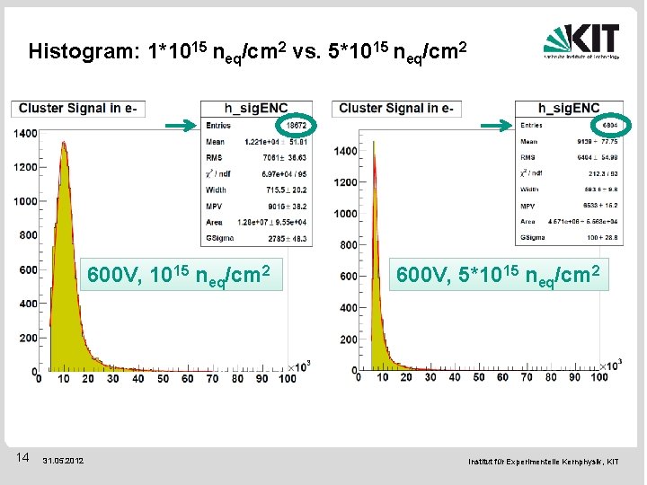
Histogram: 1*1015 neq/cm 2 vs. 5*1015 neq/cm 2 600 V, 1015 neq/cm 2 14 31. 05. 2012 600 V, 5*1015 neq/cm 2 Institut für Experimentelle Kernphysik, KIT

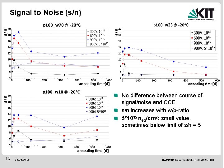
Signal to Noise (s/n) No difference between course of signal/noise and CCE s/n increases with w/p-ratio 5*1015 neq/cm 2: small value, sometimes below limit of s/n = 5 15 31. 05. 2012 Institut für Experimentelle Kernphysik, KIT

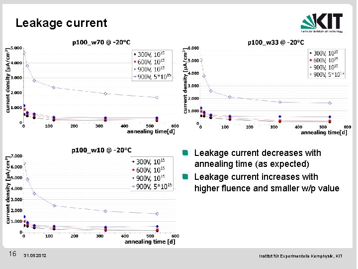
Leakage current decreases with annealing time (as expected) Leakage current increases with higher fluence and smaller w/p value 16 31. 05. 2012 Institut für Experimentelle Kernphysik, KIT

Measurement Results Pitch = 80 µm 17 31. 05. 2012 Institut für Experimentelle Kernphysik, KIT

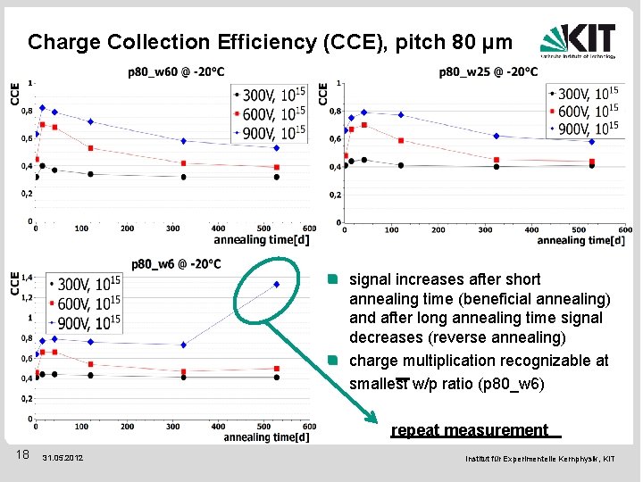
Charge Collection Efficiency (CCE), pitch 80 µm signal increases after short annealing time (beneficial annealing) and after long annealing time signal decreases (reverse annealing) charge multiplication recognizable at smallest w/p ratio (p 80_w 6) repeat measurement 18 31. 05. 2012 Institut für Experimentelle Kernphysik, KIT

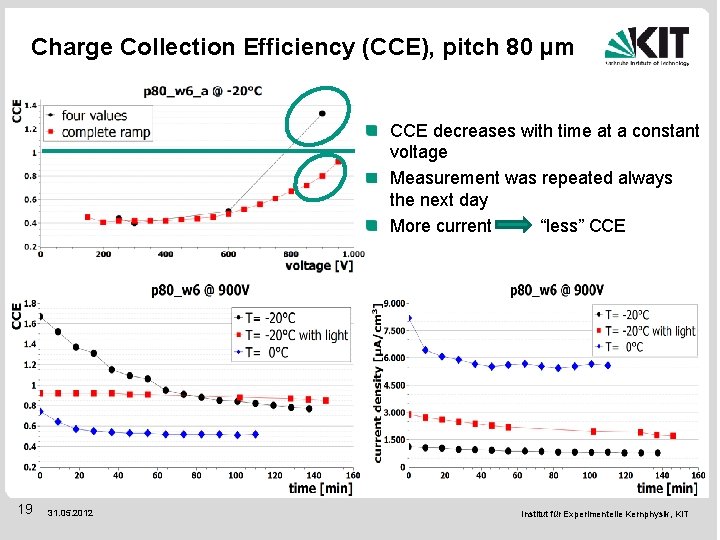
Charge Collection Efficiency (CCE), pitch 80 µm CCE decreases with time at a constant voltage Measurement was repeated always the next day More current “less” CCE 19 31. 05. 2012 Institut für Experimentelle Kernphysik, KIT

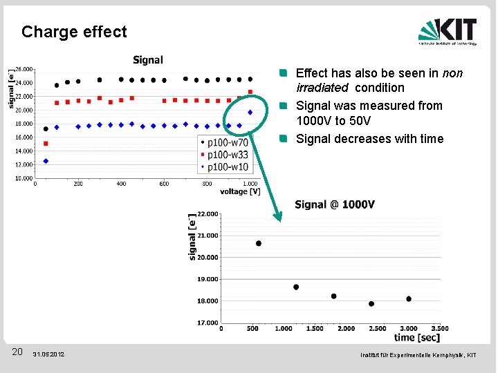
Charge effect Effect has also be seen in non irradiated condition Signal was measured from 1000 V to 50 V Signal decreases with time 20 31. 05. 2012 Institut für Experimentelle Kernphysik, KIT

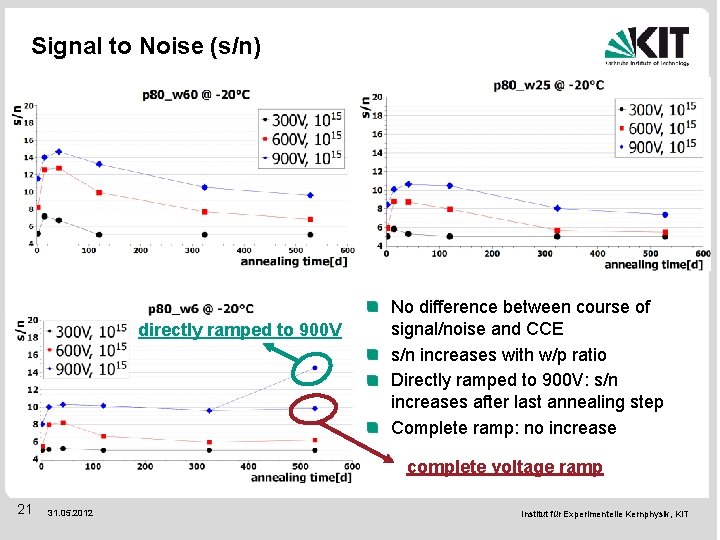
Signal to Noise (s/n) directly ramped to 900 V No difference between course of signal/noise and CCE s/n increases with w/p ratio Directly ramped to 900 V: s/n increases after last annealing step Complete ramp: no increase complete voltage ramp 21 31. 05. 2012 Institut für Experimentelle Kernphysik, KIT

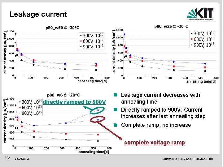
Leakage current directly ramped to 900 V Leakage current decreases with annealing time Directly ramped to 900 V: Current increases after last annealing step Complete ramp: no increase complete voltage ramp 22 31. 05. 2012 Institut für Experimentelle Kernphysik, KIT

Summary Increased charge collection for a short duration at high voltage (900 V) and a fluence of 1015 neq/cm 2 Signal to noise and leakage current also increase for a short time This effect has to be understood (perhaps more measurement with Edge TCT) No Charge Multiplication at a fluence 5*1015 neq/cm 2 so far Next step: measuring samples after neutron irradiation Dependence on processing will be investigated Sensors already measured in non irradiated condition Thanks for your attention 23 31. 05. 2012 Institut für Experimentelle Kernphysik, KIT

Backup 24 31. 05. 2012 Institut für Experimentelle Kernphysik, KIT

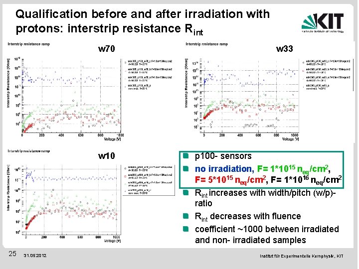
Qualification before and after irradiation with protons: interstrip resistance Rint w 70 w 10 25 31. 05. 2012 w 33 p 100 - sensors no irradiation, F= 1*1015 neq/cm 2, F= 5*1015 neq/cm 2, F= 1*1016 neq/cm 2 Rint increases with width/pitch (w/p)ratio Rint decreases with fluence coefficient ~1000 between irradiated and non- irradiated samples Institut für Experimentelle Kernphysik, KIT

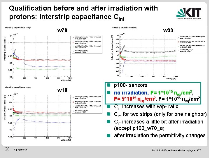
Qualification before and after irradiation with protons: interstrip capacitance Cint w 70 w 10 26 31. 05. 2012 w 33 p 100 - sensors no irradiation, F= 1*1015 neq/cm 2, F= 5*1015 neq/cm 2, F= 1*1016 neq/cm 2 Cint increases with w/p- ratio Cint for two strips (only for one neighbor) Cint increases a little bit after irradiation (except p 100_w 70_a) after irradiation the permittivity changes Institut für Experimentelle Kernphysik, KIT

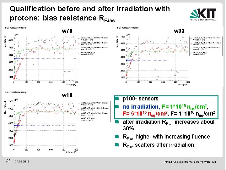
Qualification before and after irradiation with protons: bias resistance RBias w 70 w 10 27 31. 05. 2012 w 33 p 100 - sensors no irradiation, F= 1*1015 neq/cm 2, F= 5*1015 neq/cm 2, F= 1*1016 neq/cm 2 after irradiation RBias increases about 30% RBias higher with increasing fluence RBias scatters after irradiation Institut für Experimentelle Kernphysik, KIT

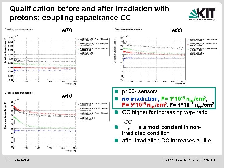
Qualification before and after irradiation with protons: coupling capacitance CC w 70 w 10 w 33 p 100 - sensors no irradiation, F= 1*1015 neq/cm 2, F= 5*1015 neq/cm 2, F= 1*1016 neq/cm 2 CC higher for increasing w/p- ratio is almost constant in nonirradiated condition after irradiation CC increases a little 28 31. 05. 2012 Institut für Experimentelle Kernphysik, KIT

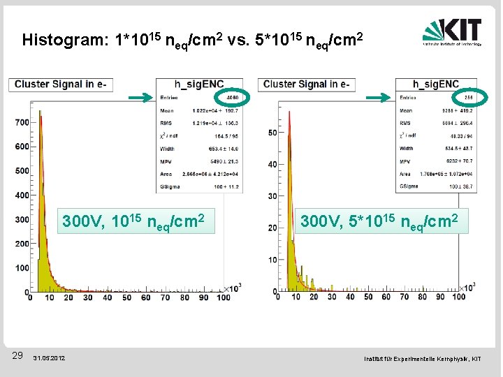
Histogram: 1*1015 neq/cm 2 vs. 5*1015 neq/cm 2 300 V, 1015 neq/cm 2 29 31. 05. 2012 300 V, 5*1015 neq/cm 2 Institut für Experimentelle Kernphysik, KIT