SVT detector electronics Mauro Villa INFN Universit di


- Slides: 15

SVT detector electronics Mauro Villa INFN & Università di Bologna Overview: - Super. B SVT open options - F. E. chips - Trigger handling

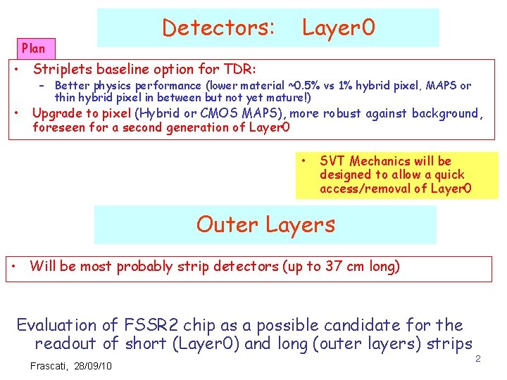
Plan Detectors: Layer 0 • Striplets baseline option for TDR: • – Better physics performance (lower material ~0. 5% vs 1% hybrid pixel, MAPS or thin hybrid pixel in between but not yet mature!) Upgrade to pixel (Hybrid or CMOS MAPS), more robust against background, foreseen for a second generation of Layer 0 • SVT Mechanics will be designed to allow a quick access/removal of Layer 0 Outer Layers • Will be most probably strip detectors (up to 37 cm long) Evaluation of FSSR 2 chip as a possible candidate for the readout of short (Layer 0) and long (outer layers) strips Frascati, 28/09/10 2

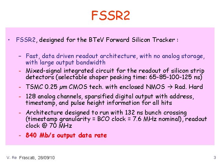
FSSR 2 • FSSR 2, designed for the BTe. V Forward Silicon Tracker : – Fast, data driven readout architecture, with no analog storage, with large output bandwidth – Mixed-signal integrated circuit for the readout of silicon strip detectors (selectable shaper peaking time: 65 -85 -100 -125 ns) – TSMC 0. 25 µm CMOS tech. with enclosed NMOS Rad. Hard – 128 analog channels, sparsified digital output with address, timestamp, and pulse height information for all hits – Architecture designed to run with 132 ns bunch crossing (timestamp granularity = BCO clock = 7. 6 MHz nominal), readout clock @ 70 MHz – 840 Mb/s output data rate V. Re Frascati, 28/09/10 3

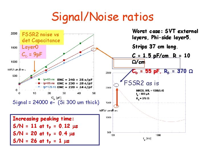
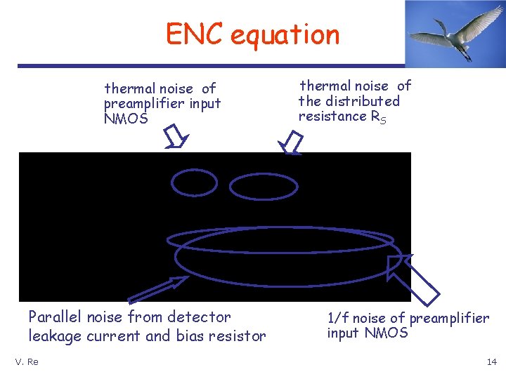
Signal/Noise ratios FSSR 2 noise vs det Capacitance Layer 0 CD = 9 p. F Worst case: SVT external layers, Phi-side layer 5. Strips 37 cm long. C = 1. 5 p. F/cm R = 10 W/cm CD = 55 p. F, RS = 370 W FSSR 2 as is Signal = 24000 e- (Si 300 um thick) Increasing peaking time: S/N = 11 at t. P = 0. 12 ms S/N = 20 at t. P = 0. 4 ms S/N = 26 at t. P = 1 ms

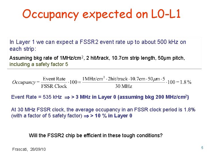
Occupancy expected on L 0 -L 1 In Layer 1 we can expect a FSSR 2 event rate up to about 500 k. Hz on each strip: Assuming bkg rate of 1 MHz/cm 2, 2 hit/track, 10. 7 cm strip length, 50μm pitch, including a safety factor 5 Event Rate = 535 k. Hz > 3 MHz in Layer 0 (assuming bkg 200 MHz/cm 2) At 30 MHz FSSR clock, the average occupancy in an FSSR clock period is 1. 8% (with a factor of 5 safety factor) > 10 % in Layer 0 Will the FSSR 2 chip be efficient in these tough conditions? Frascati, 28/09/10 5

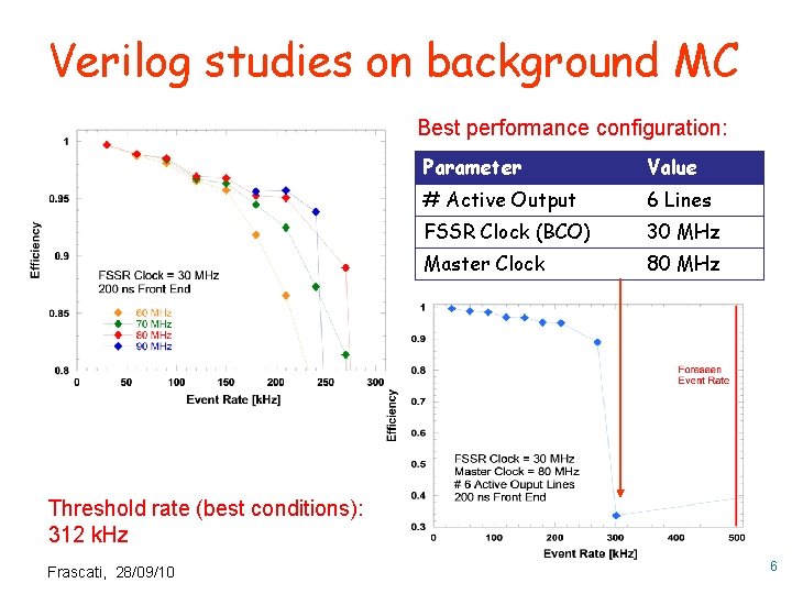
Verilog studies on background MC Best performance configuration: Parameter Value # Active Output 6 Lines FSSR Clock (BCO) 30 MHz Master Clock 80 MHz Threshold rate (best conditions): 312 k. Hz Frascati, 28/09/10 6

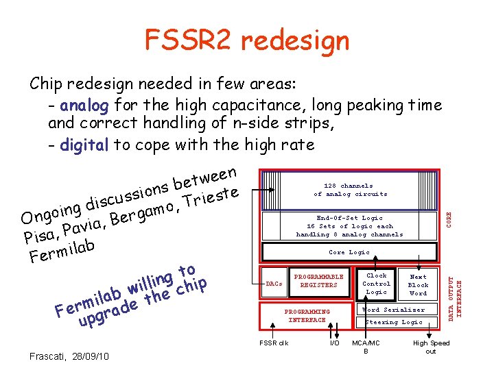
FSSR 2 redesign Chip redesign needed in few areas: - analog for the high capacitance, long peaking time and correct handling of n-side strips, - digital to cope with the high rate End-Of-Set Logic 16 Sets of logic each handling 8 analog channels Core Logic PROGRAMMABLE REGISTERS DACs Clock Control Logic Next Block Word Serializer PROGRAMMING INTERFACE FSSR clk Frascati, 28/09/10 CORE 128 channels of analog circuits Steering Logic I/O MCA/MC B DATA OUTPUT INTERFACE en e w t e b s n te sio s s e u i c r s , T di o g m n i a o rg e B Ong , a vi a P , a Pis ab l i m r Fe o t g illin chip w ab e the l i m Fer pgrad u High Speed out

FSSR 3 and other readout chips SVT Front end chips will all be triggered. We’re about to abandon the SVT trigger capabilities at least at Level 1: - Not fast enough (long peaking time) - Too demanding for available chips - Too much bandwidth needed Striplet readout (FSSR 3) will likely work in a triggerable only manner. Pixel options for L 0 will be equipped with a dual function chip (triggerable/trigger source) but will be used as triggerable. Frascati, 28/09/10

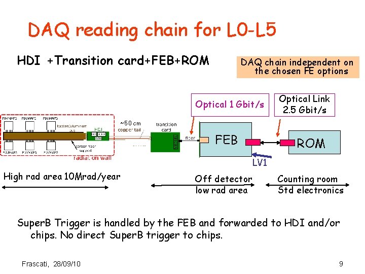
DAQ reading chain for L 0 -L 5 HDI +Transition card+FEB+ROM DAQ chain independent on the chosen FE options Optical 1 Gbit/s Optical Link 2. 5 Gbit/s ~50 cm FEB ROM LV 1 High rad area 10 Mrad/year Off detector low rad area Counting room Std electronics Super. B Trigger is handled by the FEB and forwarded to HDI and/or chips. No direct Super. B trigger to chips. Frascati, 28/09/10 9

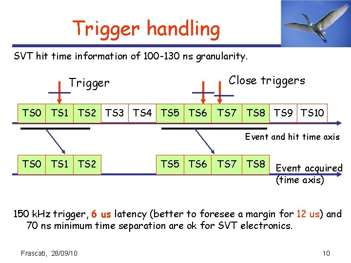
Trigger handling SVT hit time information of 100 -130 ns granularity. Trigger Close triggers TS 0 TS 1 TS 2 TS 3 TS 4 TS 5 TS 6 TS 7 TS 8 TS 9 TS 10 Event and hit time axis TS 0 TS 1 TS 2 TS 5 TS 6 TS 7 TS 8 Event acquired (time axis) 150 k. Hz trigger, 6 us latency (better to foresee a margin for 12 us) and 70 ns minimum time separation are ok for SVT electronics. Frascati, 28/09/10 10

Conclusions • Strips readout chip FSSR 2 to be redesigned • Convergence towards a triggered SVT – Better S/N ratios, higher efficiency @ high occupancy – Lower requirements on bandwidths – Contra: no trigger primitives; • Savings – Marginal saving in bandwidth on L 2 -L 5 already dominated by physics rate rather than background • 52 optical links (triggered) vs 56 O. L. (triggerable option) – No SVT Trigger processors and associated links 11


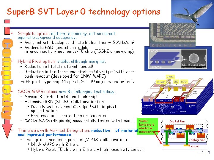
Super. B SVT Layer 0 technology options • Striplets option: mature technology, not so robust against background occupancy. – Marginal with background rate higher than ~ 5 MHz/cm 2 – Moderate R&D needed on module interconnection/mechanics/FE chip (FSSR 2 or new chip) • Hybrid Pixel option: viable, although marginal. – Reduction of total material needed! – Reduction in the front-end pitch to 50 x 50 μm 2 with data push readout (developed for DNW MAPS) FE prototype chip (4 k pixel, ST 130 nm) now under test. • CMOS MAPS option: new & challenging technology. – Sensor & readout in 50 μm thick chip! – Extensive R&D (SLIM 5 -Collaboration) on • Deep N-well devices 50 x 50μm 2 with in-pixel sparsification. • Fast readout architecture implemented – CMOS MAPS (4 k pixels) successfully tested with beams. • Wafer bonding & electrical interconn. Thin pixels with Vertical Integration: reduction of material and improved performance. – Two options are being pursued (VIPIX-Collaboration) • DNW MAPS with 2 tiers • Hybrid Pixel: FE chip with 2 tiers + high resistivity sensor Digital tier Analog tier Sensor 13 13

ENC equation thermal noise of preamplifier input NMOS Parallel noise from detector leakage current and bias resistor V. Re thermal noise of the distributed resistance RS 1/f noise of preamplifier input NMOS 14
